WO2010052870A1 - 撮像レンズ - Google Patents
撮像レンズ Download PDFInfo
- Publication number
- WO2010052870A1 WO2010052870A1 PCT/JP2009/005766 JP2009005766W WO2010052870A1 WO 2010052870 A1 WO2010052870 A1 WO 2010052870A1 JP 2009005766 W JP2009005766 W JP 2009005766W WO 2010052870 A1 WO2010052870 A1 WO 2010052870A1
- Authority
- WO
- WIPO (PCT)
- Prior art keywords
- lens
- liquid crystal
- electrode
- imaging lens
- imaging
- Prior art date
- Legal status (The legal status is an assumption and is not a legal conclusion. Google has not performed a legal analysis and makes no representation as to the accuracy of the status listed.)
- Ceased
Links
Images






Classifications
-
- G—PHYSICS
- G02—OPTICS
- G02B—OPTICAL ELEMENTS, SYSTEMS OR APPARATUS
- G02B3/00—Simple or compound lenses
- G02B3/12—Fluid-filled or evacuated lenses
- G02B3/14—Fluid-filled or evacuated lenses of variable focal length
-
- G—PHYSICS
- G02—OPTICS
- G02F—OPTICAL DEVICES OR ARRANGEMENTS FOR THE CONTROL OF LIGHT BY MODIFICATION OF THE OPTICAL PROPERTIES OF THE MEDIA OF THE ELEMENTS INVOLVED THEREIN; NON-LINEAR OPTICS; FREQUENCY-CHANGING OF LIGHT; OPTICAL LOGIC ELEMENTS; OPTICAL ANALOGUE/DIGITAL CONVERTERS
- G02F1/00—Devices or arrangements for the control of the intensity, colour, phase, polarisation or direction of light arriving from an independent light source, e.g. switching, gating or modulating; Non-linear optics
- G02F1/29—Devices or arrangements for the control of the intensity, colour, phase, polarisation or direction of light arriving from an independent light source, e.g. switching, gating or modulating; Non-linear optics for the control of the position or the direction of light beams, i.e. deflection
-
- G—PHYSICS
- G02—OPTICS
- G02F—OPTICAL DEVICES OR ARRANGEMENTS FOR THE CONTROL OF LIGHT BY MODIFICATION OF THE OPTICAL PROPERTIES OF THE MEDIA OF THE ELEMENTS INVOLVED THEREIN; NON-LINEAR OPTICS; FREQUENCY-CHANGING OF LIGHT; OPTICAL LOGIC ELEMENTS; OPTICAL ANALOGUE/DIGITAL CONVERTERS
- G02F1/00—Devices or arrangements for the control of the intensity, colour, phase, polarisation or direction of light arriving from an independent light source, e.g. switching, gating or modulating; Non-linear optics
- G02F1/29—Devices or arrangements for the control of the intensity, colour, phase, polarisation or direction of light arriving from an independent light source, e.g. switching, gating or modulating; Non-linear optics for the control of the position or the direction of light beams, i.e. deflection
- G02F1/294—Variable focal length devices
Definitions
- the present invention relates to an imaging lens including a liquid crystal lens.
- the lens function of the liquid crystal lens is set by placing the liquid crystal lens adjacent to the camera aperture in front of or behind the aperture and setting the area that functions as the lens of the liquid crystal lens to approximately the same as the aperture of the aperture.
- the area can be made a small area, and the area of the lens functional area can be reduced, so that the lens power can be increased and the focal length adjustment range can be widened (for example, , See Patent Document 1).
- a camera in which a liquid crystal lens having a focus function is arranged in an image pickup system of a camera is known (for example, see Patent Document 2). Since the focal length can be freely adjusted by changing the amount of voltage applied to the liquid crystal lens that provides this focusing function, a mechanism for adjusting the focal length by moving the lens with an actuator is not required, and the camera structure is thin. Can be.
- a light-shielding film is provided in the area excluding the lens functional area of the liquid crystal lens, and even if strong light enters the liquid crystal lens, the light is absorbed and blocked by the light-shielding film, and the strong light reaches the imaging member. Therefore, the occurrence of flare phenomenon or ghost phenomenon can be prevented.
- an imaging lens when an imaging lens is intended to increase the angle of view of an obtained image, it is generally necessary to increase the diameter of an optical system member such as a liquid crystal lens constituting the imaging lens.
- the present invention has been made in view of such circumstances, and provides an imaging lens capable of preventing a reduction in image formation performance of ambient light without increasing the diameter of a liquid crystal lens used in the imaging lens. With the goal.
- the present invention provides a front group lens disposed on the subject side, a rear group lens disposed on the image sensor side, and between two electrodes disposed between the front group lens and the rear group lens and facing each other.
- An imaging lens comprising: a liquid crystal layer having a liquid crystal layer, and a liquid crystal lens that functions as a lens by changing a refractive index distribution by controlling the orientation of liquid crystal molecules in the liquid crystal layer by applying a voltage between the opposing electrodes
- the upper and lower rays of the light beam emitted from the front group lens are made parallel to the principal ray so as to be incident on the liquid crystal lens, and the light emitted from the liquid crystal lens is emitted from the rear group lens by the rear group lens.
- An image is formed on an image sensor.
- the front lens group includes a lens having a positive power and a lens having a negative power, and a rear focal point of the lens having the positive power and a focal point of the lens having the negative power.
- a lens having the positive power and the lens having the negative power are arranged so that they substantially coincide with each other.
- the present invention is characterized in that the liquid crystal layer of the liquid crystal lens is combined with a diaphragm.
- a plurality of liquid crystal layers of the liquid crystal lens are provided with the diaphragm interposed therebetween, and liquid crystal molecules of the liquid crystal layer provided with the diaphragm sandwiched are aligned at 90 degrees with respect to each other. It is characterized by making directional light available.
- each of the liquid crystal layers provided across the diaphragm includes two liquid crystal layers.
- the present invention is characterized in that the two electrodes facing each other are composed of a first electrode having a circular notch and a substantially circular second electrode arranged at an interval in the circular portion.
- the present invention is characterized in that the first electrode is divided into four parts.
- the present invention is characterized in that the diameter of the liquid crystal lens is equal to or larger than the tangent of the incident angle multiplied by twice the distance from the electrode to the liquid crystal layer plus the diameter of the diaphragm. To do.
- the present invention is characterized in that the liquid crystal lens has a diameter of 1 mm or more and 4 mm or less.
- the present invention is characterized in that a liquid crystal film aligned in parallel is disposed immediately after the liquid crystal lens.
- the present invention is characterized in that a parallel oriented liquid crystal film is disposed after the rear lens group.
- the present invention since the upper ray and the lower ray of the light beam incident on the liquid crystal lens are parallel to the principal ray, there is no need to increase the diameter of the liquid crystal lens even when the angle of view is large. It is possible to prevent an increase in thickness and an increase in applied voltage. In addition, there is an effect that it is possible to prevent the imaging performance of the ambient light from being deteriorated even when the angle of view for imaging is increased.
- FIG. 1 is a diagram showing a configuration of the embodiment.
- reference numeral 100 denotes an imaging lens, which comprises a front group lens 1 disposed on the subject side, a liquid crystal lens 2 and a rear group lens 3 disposed on the imaging element 5 side.
- Reference numeral 4 denotes a cover glass that protects the image sensor 5.
- the front lens group 1 includes a first lens 11 and a second lens 12.
- the rear group lens 3 includes a third lens 31, a fourth lens 32, and a fifth lens 33.
- a light beam from a subject travels so that a principal ray intersects at the center of the stop of the imaging lens by the front lens group 1 and enters the liquid crystal lens 2.
- the light beam transmitted through the liquid crystal lens 2 is collected by the rear group lens 3, passes through the cover glass 4, and forms an image on the light receiving surface of the image sensor 5.
- an image of the subject is formed on the light receiving surface of the image sensor 5 by the imaging lens 100.
- the image sensor 5 photoelectrically converts the intensity of the imaged light, and the obtained electric signal is image-processed to generate a digital image.
- the front lens group 1 shown in FIG. 1 is composed of two lenses, the first lens 11 is a convex lens having a positive power, and the second lens 12 is a concave lens having a negative power.
- the group lens 1 as a whole constitutes a lens having positive power.
- the rear focal point f1 of the first lens 11 and the front focal point f2 of the second lens 12 are arranged so as to substantially coincide. For this reason, in the light from the subject that enters the first lens 11 and exits from the second lens 12, the upper ray a and the lower ray b are parallel to the principal ray c.
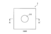
- FIGS. 3 and 4 are a front view and a cross-sectional view showing the configuration of the liquid crystal lens 2 shown in FIG.
- the center of the liquid crystal lens 2 has a substantially circular physically unique portion 215 described in detail below.
- the liquid crystal lens 2 includes a transparent first electrode 201 and a second electrode 202, a transparent third electrode 203, a transparent fourth electrode 204, and a first electrode 201 and a third electrode 203 in the same layer.
- the second liquid crystal layer 212 disposed between the third insulating layers 207, the third liquid crystal layer 213 disposed between the fourth insulating layer 208 and the fifth insulating layer 209, and the fifth insulating layer 209.
- the first electrode 201 shown in FIG. 4 includes a circular cutout portion in which a central portion of a transparent and conductive thin film (for example, made of ITO (indium tin oxide)) is cut out in a circular shape, It has a strip cutout part in which a partial strip of the membrane is cut out.
- the circular notch communicates with the outside through the strip notch.
- the first electrode 201 is an electrode for applying a voltage to the outside of the circular opening.
- the second electrode 202 is formed of a circular transparent and conductive thin film, and a transparent and conductive strip 202a is added to a part of the outer periphery of the electrode so as to maintain conductivity.
- the second electrode 202 and the strip 202a are stored in the circular notch and the partial strip notch of the first electrode 201 with a space therebetween.
- the second electrode 202 is an electrode for applying a voltage inside the circular opening.
- the first electrode 201 and the second electrode 202 have a structure in which an independent voltage can be applied to each electrode.
- liquid crystal molecules (for example, nematic liquid crystal molecules) of the first liquid crystal layer 211 and the third liquid crystal layer 213 are aligned in the same direction (for example, an alignment direction A of 45 degrees as shown in FIG. 5).
- the liquid crystal molecules of the second liquid crystal layer 212 and the fourth liquid crystal layer 214 are aligned with the orientation direction of the liquid crystal molecules of the first liquid crystal layer 211 and the third liquid crystal layer 213 from the electrode 203 side with the center of the circular opening as the center. Since the liquid crystal lens 2 is oriented in a direction rotated 90 degrees clockwise (for example, the orientation direction B shown in FIG. 5) and can use both the P-polarized wave and the S-polarized wave, the liquid crystal lens 2 can emit light in any vibration direction.
- the liquid crystal lens 2 shown in FIG. 4 has a structure that is symmetrical in the thickness direction with respect to the second electrode 202, and has a structure having two layers in each vibration direction for high speed.
- the diameter of the circular outer shape of the second electrode 202 is about 3 mm.
- the thicknesses of the third insulating layer 207 and the fourth insulating layer 208 are determined from the diameter of the circular opening and are 700 ⁇ m. If the thickness of the second insulating layer 206 and the fifth insulating layer 209 is large, the positional deviation of the imaging position in the optical axis direction of the two-polarized liquid crystal lens 2 different by 90 degrees becomes large, and the imaging performance of the imaging optical system is increased. It is better to be as thin as possible because it gets worse.
- the thickness of the second insulating layer 206 and the fifth insulating layer 209 is 70 ⁇ m.
- the thicknesses of the first insulating layer 205 and the sixth insulating layer 210 also affect the thickness of the liquid crystal lens 2, and the imaging performance of the imaging lens 100 is improved as thin as possible.
- glass or the like is preferably used as a material for the insulating layer because it needs to transmit visible light.
- an ITO (Indium Tin Oxide) film which is a transparent conductive film, is applied to the surface of the glass thin plate. Formed by sputtering.
- the first electrode 201 may be an ITO film deposited on the surface of a glass thin plate used in the production of the second electrode, or a metal thin film such as aluminum.
- the operation of the liquid crystal lens 2 shown in FIGS. 3 and 4 will be described.
- the central axis of the first electrode 201 having a circular opening is provided.
- An electric field subject to an axis is generated for 220.
- Liquid crystal molecules in the first liquid crystal layer 211, the second liquid crystal layer 212, the third liquid crystal layer 213, and the fourth liquid crystal layer 214 are aligned along the generated electric field.
- the liquid crystal molecules have birefringence, and the refractive index in the major axis direction and the refractive index in the minor axis direction of the elliptical liquid crystal molecules are different.
- the voltage applied to the first electrode 201 is V1
- the voltage applied to the second electrode 202 is V2
- the voltage applied to the third electrode 203 is V3
- the voltage applied to the fourth electrode 204 is V4, and V3
- V4 and V4 ⁇ V2 ⁇ V1 the director direction of the liquid crystal layer (the average alignment direction of the liquid crystal molecules) changes as shown in FIG. Thereby, the angle of the liquid crystal molecules changes from the central axis 220 to the periphery of the first electrode 201 having a circular opening, and a refractive index distribution is generated.
- the refractive index at the center is higher than the refractive index at the periphery, and the distribution of one cross section passing through the center becomes a characteristic close to a quadratic curve, so that it acts as a refractive index distribution lens having a positive power.
- the focal length of the liquid crystal lens 2 can be changed by adjusting the voltage applied to the first electrode 201 and the second electrode 202, it can also function as a variable focus lens.
- the voltage applied to the first electrode 201 is V1
- the voltage applied to the second electrode 202 is V2
- the voltage applied to the third electrode 203 is V3
- the voltage applied to the fourth electrode 204 is V4.
- the refractive index at the center is lower than the refractive index at the periphery, and the distribution of one cross section passing through the center is close to a quadratic curve. Therefore, it can function as a variable focus lens having negative power. It becomes.
- an effective voltage of 20 Vrms (rms: root mean square value) is applied between the first electrode 201 and the second electrode 202, and the second electrode 202 and the third and fourth electrodes 203
- An effective voltage of 70 Vrms is applied between the first electrode 201 and the effective voltage of 90 Vrms is applied between the first electrode 201 and the third and fourth electrodes 203 and 204 to function as a convex lens.
- the liquid crystal driving voltage (voltage applied between the electrodes) is a sine wave or a rectangular wave AC waveform with a duty ratio of 50%.
- an AC sine wave of 100 Vrms has a voltage waveform having a peak value of ⁇ 144V. Further, for example, 1 kHz is used as the frequency of the AC voltage.
- the focal length of the liquid crystal lens 2 is determined by the refractive index distribution due to the change in the director direction of the in-plane liquid crystal layer, the maximum value is determined by the birefringence of the liquid crystal molecules, and the above voltage value is applied.
- the focal length is about 200 mm. Since the focal length of the imaging lens 100 shown in FIG. 1 is about 7 mm, the power of the liquid crystal lens 2 is about 3% of the power of the imaging lens 100. For this reason, the refractive power of the liquid crystal lens 2 alone is small.
- the refraction angle of the light beam incident from the front lens group 1 in the first liquid crystal layer 211 is as small as about 0.5 degrees, the upper light beam, the main light beam, and the lower light beam incident from the front lens group 1 are in a substantially parallel state.
- the light is emitted from the liquid crystal lens 2.
- the diameter of the liquid crystal lens 2 used as a lens is increased, the third insulating layer 208 and the fourth insulating layer 209 need to be thickened, so that the length of the imaging lens 100 increases.
- the diameter of the liquid crystal lens 2 (the diameter of the circular outer shape of the electrode 202) is preferably set to ⁇ 1 mm to ⁇ 4 mm. .
- the circular aperture stop 215 since the circular aperture stop 215 is in the vicinity of the first electrode 201 and the second electrode 202, it is necessary to have an insulating property and not to transmit visible light.
- a chromium oxide (Cr 2 O 3) film or the like can be used.
- the rear lens group 3 shown in FIG. 1 includes a third lens 31 having a concave power, a fourth lens 32 having a positive power, and a fifth lens 33 having a positive power. Further, the third lens 31 and the fourth lens 32 are bonded lenses.
- the third lens 31 has a high dispersion glass material (with a small Abbe number), and the fourth lens 32 has a low dispersion glass material (with an Abbe number). It is possible to correct chromatic aberration.
- the diameter of the circular aperture stop 215 in the liquid crystal lens 2 is D1
- the focal length of the rear group lens 3 is f2
- the F number of the imaging lens 100 is F.
- the incident angle of the light beam to the circular aperture stop 215 in the liquid crystal lens 2 is ⁇ [rad]
- the distance from the first electrode 201 to the first liquid crystal layer 211 is T
- the diameter of the liquid crystal lens 2 (the diameter of the circular outer shape of the electrode 202) is DL, DL ⁇ f2 / F + 2T ⁇ tan ⁇ Is desirable.
- the diameter DL of the liquid crystal lens 2 is desirably 1 mm to 4 mm, 1 ⁇ f2 / F + 2T ⁇ tan ⁇ ⁇ 4 Is desirable.
- FIG. 9 shows an example of the MTF curve at the screen center and the periphery of the screen when DL ⁇ f2 / F + 2T ⁇ tan ⁇ .
- FIG. 10 shows an example of the MTF curve at the screen center and the periphery of the screen when DL ⁇ f2 / F + 2T ⁇ tan ⁇ .
- the horizontal axis represents the spatial frequency
- the vertical axis represents MTF as a percentage.
- the fifth lens 33 may have an aspheric surface (both surfaces). By using the aspherical lens, the light beam from one point on the object plane is most separated on the lens curved surface of the fifth lens 33, so that it becomes easy to correct the aberration.
- the first lens 11 may be an aspheric lens.
- a part or all of the imaging lens 100 may be an aspherical lens. In the present embodiment, the imaging lens is described as having five lenses. However, it is possible to increase the number of lenses to improve performance or to reduce the thickness.
- the upper ray and the lower ray of the light beam incident on the liquid crystal lens 2 are parallel to the principal ray, it is not necessary to increase the diameter of the liquid crystal lens 2 even when the angle of view is large. An increase in thickness and an increase in applied voltage can be prevented. In addition, it is possible to prevent the imaging performance of ambient light from deteriorating even when the angle of view for imaging is increased.
- FIG. 11 is a diagram illustrating a configuration of the liquid crystal lens 2 according to the second embodiment.
- the liquid crystal lens 2 shown in FIG. 11 is different from the liquid crystal lens 2 shown in FIG. 3 in that the first electrode 201 of the liquid crystal lens 2 is divided into four in the vertical and horizontal directions, and the electrode 201a, electrode 201b, electrode 201c, and electrode 201d are divided. It is a point provided.
- the refractive index distribution that was an axis object when the electrodes were not divided was The distribution can be changed to an asymmetric distribution with the axis shifted from the center axis. This is equivalent to moving the optical axis of the liquid crystal lens 2.
- the incident light to the liquid crystal lens 2 can be deflected.
- the amount of incident light deflected can be changed by appropriately changing the voltages applied to the electrodes 201a, 201b, 201c, and 201d.
- the power of the liquid crystal lens 2 is about 3% of the power of the entire imaging lens 100, an optical axis shift amount of about 3% of the optical axis shift amount of the liquid crystal lens 2 can be obtained.
- liquid crystal molecules of the first liquid crystal layer 211 and the third liquid crystal layer 213 are aligned in the same direction (for example, the 45-degree alignment direction A shown in FIG. 5), and the second liquid crystal layer 212
- the liquid crystal molecules of the fourth liquid crystal layer 214 are rotated by 90 degrees clockwise about the center of the circular opening (for example, the alignment direction of the liquid crystal molecules of the first liquid crystal layer 211 and the third liquid crystal layer 213 (for example, It is oriented in the orientation direction B) shown in FIG. It is desirable that the alignment direction A and the alignment direction B shown in FIG. 11 do not coincide with the dividing direction in which the first electrode 201 is divided into four electrodes 201a, 201b, 201c, and 201d.
- FIG. 12 is a diagram showing a positional shift of the focal point in the optical axis direction of two polarized light different from each other by 90 degrees, which is generated depending on the thicknesses of the second insulating layer 206 and the fifth insulating layer 209 of the liquid crystal lens 2.
- Polarized light in the same vibration direction as the alignment direction of the liquid crystal layer 211 and the liquid crystal layer 213 is refracted by the lens effect of the liquid crystal layer 211 and the liquid crystal layer 213 and has a focal point as shown in FIG.
- the alignment directions of the liquid crystal layer 212 and the liquid crystal layer 214 are rotated by 90 degrees, they do not have a lens effect and pass through.
- the polarized light in the direction rotated by 90 degrees with the polarized light (polarized light having the same vibration direction as the alignment direction of the liquid crystal layer 212 and the liquid crystal layer 214) is refracted by the lens effect of the liquid crystal layer 212 and the liquid crystal layer 214, and is shown in FIG. So focus.
- the alignment direction of the liquid crystal layer 211 and the liquid crystal layer 213 is rotated by 90 degrees, the liquid crystal layer 211 and the liquid crystal layer 213 transmit without having a lens effect. That is, the two orthogonally polarized lights are refracted by a lens having a different position and have a focal point, so that a focal position shift occurs.
- the focal position shift causes image blur on the image sensor 5.
- a very large birefringence is required. Therefore, it is preferable to dispose a liquid crystal film aligned in parallel. Since the liquid crystal molecules in the liquid crystal film are fixed at a predetermined angle and birefringence is given between ordinary light and extraordinary light, the phases of the two orthogonally polarized lights can be changed. The positional deviation can be corrected.
- the birefringence of the liquid crystal is usually about 0.2. Therefore, in order to correct the focal position deviation of 70 ⁇ m, the thickness may be 350 ⁇ m.
- a liquid crystal film 6 may be provided after the rear lens group 3.
- the power of the liquid crystal lens 2 is about 3% of the power of the imaging lens 100, so that the liquid crystal film 6 is provided after the rear lens group 3 to make the liquid crystal film 6 thinner. It is possible to correct the focal position shift.
- the birefringent material for correcting the misalignment of the focal point in the optical axis direction of two polarized light different by 90 degrees is not limited to the liquid crystal film.
- a birefringent plastic film, crystal, sapphire glass, or the like may be used.
Landscapes
- Physics & Mathematics (AREA)
- General Physics & Mathematics (AREA)
- Optics & Photonics (AREA)
- Nonlinear Science (AREA)
- Liquid Crystal (AREA)
- Lenses (AREA)
Abstract
被写体側に配置される前群レンズと、撮像素子側に配置される後群レンズと、前群レンズと後群レンズの間に配置され、互いに対向する2つの電極の間に液晶層を有し、対向する電極間に電圧を印加することにより液晶層の液晶分子の配向制御を行うことにより屈折率分布を変化させて液晶レンズとして機能させる液晶レンズとを備える撮像レンズであって、前群レンズから出射する光束の上光線と下光線が主光線と平行になるようにして、液晶レンズへ入射させ、後群レンズにより液晶レンズからの出射光を撮像素子に結像させる。この構成により、撮像レンズ内に用いる液晶レンズを大口径化させることなく周辺光の結像性能が低下を防止することができる。
Description
本発明は、液晶レンズを備える撮像レンズに関する。
本願は、2008年11月05日に、日本に出願された特願2008-284198号に基づき優先権を主張し、その内容をここに援用する。
本願は、2008年11月05日に、日本に出願された特願2008-284198号に基づき優先権を主張し、その内容をここに援用する。
従来から、カメラの撮像光学系内に液晶レンズを配置する撮像レンズが提案されている。例えば、液晶レンズをカメラの絞りに隣接して絞りの前、あるいは絞りの後に配置し、液晶レンズのレンズとして機能する領域を絞りの開口量とほぼ同じ位に設定することで液晶レンズのレンズ機能領域を小さい面積の領域にすることができ、また、レンズ機能領域の面積が小さくなることにより、レンズパワーを高めることができて、焦点距離の調整範囲を広くすることができるものがある(例えば、特許文献1参照)。
また、カメラの撮像系にフォーカス機能を有する液晶レンズを配設したものが知られている(例えば、特許文献2参照)。このフォーカス機能が得られる液晶レンズに印加する電圧量を変化させることによって自由に焦点距離の調整ができるため、レンズをアクチュエータによって移動させて焦点距離を調整する機構が不要となり、カメラの構造を薄型にすることができる。また、液晶レンズのレンズ機能領域を除いた領域部分に遮光膜を設け、液晶レンズ内に強い光が入ってもその遮光膜により光を吸収して遮り、強い光が結像部材に届くのを防止してフレア現象やゴースト現象などの発生を防止することができる。
ところで、撮像レンズは、得られる画像の画角を大きくしようとする場合、一般的に撮像レンズを構成する液晶レンズ等の光学系部材を大口径化する必要がある。
しかしながら、撮像レンズ内に用いる液晶レンズの大口径化は液晶ガラスの厚みの増大、印加電圧の増大を招き、更に液晶レンズの焦点距離も長くなるという問題がある。また撮像する画角が大きくなると周辺光の結像性能が低下してしまうという問題もある。
本発明は、このような事情に鑑みてなされたもので、撮像レンズ内に用いる液晶レンズを大口径化させることなく周辺光の結像性能が低下を防止することができる撮像レンズを提供することを目的とする。
本発明は、被写体側に配置される前群レンズと、撮像素子側に配置される後群レンズと、前記前群レンズと前記後群レンズの間に配置され、互いに対向する2つの電極の間に液晶層を有し、前記対向する電極間に電圧を印加することにより前記液晶層の液晶分子の配向制御を行うことにより屈折率分布を変化させてレンズとして機能させる液晶レンズとを備える撮像レンズであって、前記前群レンズから出射する光束の上光線と下光線が主光線と平行になるようにして、前記液晶レンズへ入射させ、前記後群レンズにより前記液晶レンズからの出射光を前記撮像素子に結像させることを特徴とする。
本発明は、前記前群レンズは、正のパワーを持つレンズと、負のパワーを持つレンズとから構成し、前記正のパワーを持つレンズの後側焦点と前記負のパワーを持つレンズの焦点が略一致するように、前記正のパワーを持つレンズと前記負のパワーを持つレンズを配置したことを特徴とする。
本発明は、前記液晶レンズの液晶層は、絞りと組み合わされていることを特徴とする。
本発明は、前記液晶レンズの液晶層は、前記絞りを挟んで複数設けられており、かつ前記絞りを挟んで設けられた液晶層の液晶分子は互いに90度ずれて配向しており、あらゆる振動方向の光を利用可能にすることを特徴とする。
本発明は、前記絞りを挟んで設けられた液晶層は、それぞれ2つの液晶層からなることを特徴とする。
本発明は、前記互いに対向する2つの電極は、円形の切欠きを有する第1の電極と、前記円形部分に間隔を置いて配置された略円形状の第2の電極とからなることを特徴とする。
本発明は、前記第1の電極は、4分割されていることを特徴とする。
本発明は、前記液晶レンズの直径は、入射角の正接に前記電極から前記液晶層までの距離の2倍を掛けたものに前記絞りの直径を加えたものに等しいかより大きいことを特徴とする。
本発明は、前記液晶レンズの直径は、1mm以上4mm以下であることを特徴とする。
本発明は、前記液晶レンズの直後に平行配向した液晶フィルムを配置したことを特徴とする。
本発明は、前記後群レンズの後に平行配向した液晶フィルムを配置したことを特徴とする。
本発明によれば、液晶レンズへ入射する光束の上光線と下光線が主光線と平行になるため、画角が大きい場合であっても液晶レンズを大口径化する必要がなくなり、液晶ガラスの厚みの増大、印加電圧の増大を防止することができるという効果が得られる。また撮像する画角が大きくなっても周辺光の結像性能が低下してしまうことを防止することができるという効果も得られる。
<第1の実施形態>
以下、本発明の第1の実施形態による撮像レンズを図面を参照して説明する。図1は同実施形態の構成を示す図である。この図において、符号100は、撮像レンズであり、被写体側に配置される前群レンズ1、液晶レンズ2及び撮像素子5側に配置される後群レンズ3から構成する。符号4は、カバーガラスであり、撮像素子5を保護する。撮像素子5には、CCD(Charge Coupled Device)センサやCMOS(Complementary Metal Oxide Semiconductor)センサなどを用いる。前群レンズ1は、第1のレンズ11、第2のレンズ12で構成する。後群レンズ3は、第3のレンズ31、第4のレンズ32及び第5のレンズ33で構成する。被写体(図示せず)からの光束は、前群レンズ1によって撮像レンズの絞り中心で主光線が交わるように進行し、液晶レンズ2に入射する。液晶レンズ2を透過し射出した光束は、後群レンズ3により集光され、カバーガラス4を透過し撮像素子5の受光面に結像される。これにより、撮像素子5の受光面には、撮像レンズ100によって、被写体の像が結像することになる。撮像素子5は、この結像された光の強弱を光電変換し、得られた電気信号は画像処理して、デジタル画像を生成する。
以下、本発明の第1の実施形態による撮像レンズを図面を参照して説明する。図1は同実施形態の構成を示す図である。この図において、符号100は、撮像レンズであり、被写体側に配置される前群レンズ1、液晶レンズ2及び撮像素子5側に配置される後群レンズ3から構成する。符号4は、カバーガラスであり、撮像素子5を保護する。撮像素子5には、CCD(Charge Coupled Device)センサやCMOS(Complementary Metal Oxide Semiconductor)センサなどを用いる。前群レンズ1は、第1のレンズ11、第2のレンズ12で構成する。後群レンズ3は、第3のレンズ31、第4のレンズ32及び第5のレンズ33で構成する。被写体(図示せず)からの光束は、前群レンズ1によって撮像レンズの絞り中心で主光線が交わるように進行し、液晶レンズ2に入射する。液晶レンズ2を透過し射出した光束は、後群レンズ3により集光され、カバーガラス4を透過し撮像素子5の受光面に結像される。これにより、撮像素子5の受光面には、撮像レンズ100によって、被写体の像が結像することになる。撮像素子5は、この結像された光の強弱を光電変換し、得られた電気信号は画像処理して、デジタル画像を生成する。
次に、図2を参照して、図1に示す前群レンズ1の構成について説明する。図2に示すように、前群レンズは2枚のレンズで構成されており、第1のレンズ11は正のパワーを持つ凸レンズ、第2のレンズ12は負のパワーを持つ凹レンズであり、前群レンズ1全体としては正のパワーを持つレンズを構成している。第1のレンズ11の後側焦点f1と第2のレンズ12の前側焦点f2は略一致するように配置されている。このため、第1のレンズ11に入射して第2のレンズ12から射出する被写体からの光は、上光線aと下光線bのそれぞれが主光線cに該平行になる。なお、色収差の補正のためには、第1のレンズ11に低分散硝材(アッベ数が大)、第2のレンズ12に高分散硝材(アッベ数が小)を用いることが望ましい。
次に、図3~図7を参照して、図1に示す液晶レンズ2の構成について説明する。図3、図4は、図1に示す液晶レンズ2の構成を示す正面図と断面図である。図3の正面図に示すように、液晶レンズ2の中央には以下に詳説する略円形の物理的に特異な部分215を有する。液晶レンズ2は、同一層にある透明な第1の電極201と第2の電極202、透明な第3の電極203、透明な第4の電極204、第1の電極201と第3の電極203の間に配置された第1の絶縁層205、第2の絶縁層206、第3の絶縁層207、第1の電極201と、第4の電極204の間に配置された第4の絶縁層208、第5の絶縁層209、第6の絶縁層210、第1の絶縁層205と第2の絶縁層206の間に配置された第1の液晶層211、第2の絶縁層206と第3の絶縁層207の間に配置された第2の液晶層212、第4の絶縁層208と第5の絶縁層209の間に配置された第3の液晶層213、第5の絶縁層209と第6の絶縁層210の間に配置された第4の液晶層214、第1の電極201、第2の電極202に接して配置され絶縁遮光層で作成された円形開口の絞り215によって構成されている。
図4に示す第1の電極201は、図5に示すように、透明かつ導電性の薄膜(例えば、ITO(酸化インジウム錫)からなる)の中央部分を円形に切り欠いた円形切欠部と、膜の一部細片を切り欠いた細片切欠部を有する。円形切欠部は、細片切欠部を通して外部に通じている。第1の電極201は、円形開口の外側に電圧を印加するための電極である。また、第2の電極202は、円形状の透明かつ電導性の薄膜からなり、この電極の外周の一部には透明かつ電導性の細片202aが導通性を保つ状態で付加されている。第2の電極202および細片202aは、第1の電極201の円形切欠部及び一部細片切欠部に間隔を空けて収められている。第2の電極202は、円形開口の内側に電圧を印加するための電極である。第1の電極201と第2の電極202は、それぞれの電極に独立した電圧を印加することができる構造となっている。
また、第1の液晶層211と第3の液晶層213の液晶分子(例えば、ネマチック液晶分子)は、同一方向(例えば、図5に示す斜め45度の配向方向A)に配向されており、第2の液晶層212と第4の液晶層214の液晶分子は、第1の液晶層211と第3の液晶層213の液晶分子の配向方向を、円形開口の中心を中心として電極203側から見て時計回りに90度回転した方向(例えば、図5に示す配向方向B)に配向されており、P偏光波とS偏光波の両者を利用できるので、液晶レンズ2はあらゆる振動方向の光に対してレンズとして機能することが可能である。図5に示す配向方向A及び配向方向Bは、第1の電極201の引き出し部202aが延びる方向と一致していないことが望ましい。なお、図4に示す液晶レンズ2は、第2の電極202に対して厚み方向に対称な構造となっており、高速化のため各振動方向に2層ずつの層を有する構造としている。
次に、図4に示す液晶レンズ2の寸法の一例を示す。第2の電極202の円形状外形の径は約3mmである。第3の絶縁層207と第4の絶縁層208の厚さは、円形開口の径から決定するものであり、700μmである。第2の絶縁層206と第5の絶縁層209の厚みが大きいと90度異なる2偏光の液晶レンズ2の光軸方向の結像位置の位置ずれが大きくなり、撮像光学系の結像性能が悪くなるため、なるべく薄いほうが良い。ここでは、第2の絶縁層206と第5の絶縁層209の厚みを70μmとしている。第1絶縁層205と第6の絶縁層210の厚みも液晶レンズ2の厚みに影響し、なるべく薄いほうが撮像レンズ100の結像性能が良くなるため、ここでは500μmとしている。なお、絶縁層の材料には、可視光を透過する必要があるため、ガラスなどを用いるのがよい。
また、第2の電極202、第3の電極203、第4の電極204は可視光を透過する必要があるため、透明導電膜であるITO(Indium Tin Oxide)膜等をガラス薄板の表面に対してスパッタリングを用いて形成されている。第1の電極201は、第2の電極作成の際に用いたガラス薄板の表面に蒸着したITO膜でもよいし、アルミニウム等の金属薄膜でもよい。
次に、図3、図4に示す液晶レンズ2の動作を説明する。円形開口を持つ第1の電極201と、第2の電極202と、第3の電極203、第4の電極204の間に電位差を与えることにより、円形開口を有する第1の電極201の中心軸220に対して軸対象な電界が発生する。第1の液晶層211、第2の液晶層212、第3の液晶層213、第4の液晶層214中の液晶分子は、発生した電界に沿って配向する。液晶分子は、複屈折性を持っており、楕円形をした液晶分子の長軸方向の屈折率と、短軸方向の屈折率が異なる。通常、楕円形をした液晶分子では、「短軸方向の屈折率>長軸方向の屈折率」となる。
第1の電極201に印加する電圧をV1、第2の電極202に印加する電圧をV2、第3の電極203に印加する電圧をV3、第4の電極204に印加する電圧をV4とし、V3=V4、V4<V2<V1となるように各電圧を印加すると、図6に示すように液晶層のダイレクタ方向(液晶分子の平均的な配向方向)が変化する。これにより、円形開口を有する第1の電極201の中心軸220から周辺にかけて液晶分子の角度が変化して、屈折率分布が発生する。このとき中心の屈折率のほうが周辺の屈折率より高く、その中心を通る一断面の分布が2次曲線に近い特性となることから、正のパワーを持つ屈折率分布レンズとしての作用を持つ。
また、第1の電極201と第2の電極202に印加する電圧を調整することにより、液晶レンズ2の焦点距離を変えることができるため、可変焦点レンズとして機能させることも可能である。また、第1の電極201に印加する電圧をV1、第2の電極202に印加する電圧をV2、第3の電極203に印加する電圧をV3、第4の電極204に印加する電圧をV4とし、V3=V4、V4<V1<V2となるように電圧を印加すると、円形開口を有する第1の電極201の中心軸220から周辺にかけて液晶分子の角度が変化して屈折率分布が発生する。このとき中心の屈折率のほうが周辺の屈折率より低く、その中心を通る一断面の分布が2次曲線に近い特性となることから、負のパワーをもつ可変焦点レンズとしての機能させることも可能となる。
ここでは、第1の電極201と第2の電極202の間に20Vrms(rms:root mean square value)の実効電圧を印加し、また、第2の電極202と第3、第4の電極203、204の間に70Vrmsの実効電圧を印加し、第1の電極201と第3、第4の電極203、204の間には90Vrmsの実効電圧を印加し、凸レンズとして機能させる。液晶駆動電圧(各電極間に印加する電圧)は正弦波、またはデューティ比50%の矩形波の交流波形である。例えば100Vrmsの交流正弦波は、±144Vの尖頭値を有する電圧波形となる。また、交流電圧の周波数は例えば1kHzが用いられる。
このように、液晶レンズ2の焦点距離は面内の液晶層のダイレクタ方向の変化による屈折率分布で決定されるため、液晶分子の複屈折でその最大値が決まり、上記の電圧値を印加したときの焦点距離は約200mmとなる。図1に示す撮像レンズ100の焦点距離は約7mmであるため、液晶レンズ2のパワーは撮像レンズ100のパワーの約3%である。このため、液晶レンズ2単体での屈折力は小さい。前群レンズ1から入射した光束の第1の液晶層211での屈折角度は約0.5度と小さいため、前群レンズ1から入射した上光線、主光線、下光線はほぼ平行な状態で、液晶レンズ2から出射する。液晶レンズ2はレンズとして利用する径を大きくすると、第3の絶縁層208と、第4の絶縁層209を厚くする必要があるため、撮像レンズ100の長さが増大する。更にそれに伴い第1の電極201、第2の電極202への印加電圧も高くする必要があるため、液晶レンズ2の径(電極202の円形状外形の径)はφ1mm~φ4mmとすることが望ましい。
このことから、図7に示すように、液晶レンズ2の第1の電極202付近に、中心に円形の開口を有する開口絞り215を液晶レンズ2の中心軸220に合わせて配置することにより、第1の液晶層211と第4の液晶層214、第2の液晶層212と第3の液晶層213を透過する光束径をほぼ同じにすることができ、このとき液晶層を透過する光束径が最小となる。ここで、円形開口絞り215は、第1の電極201、第2の電極202の近傍にあるため絶縁性を持ち、かつ可視光を透過しないことが必要であり、チタン系黒色顔料や、絶縁性の酸化クロム(Cr2O3)膜などを用いることができる。
次に、図1に示す後群レンズ3について説明する。後群レンズ3は、図8に示すように凹のパワーを持つ第3のレンズ31と正のパワーを持つ第4のレンズ32、正のパワーを持つ第5のレンズ33により構成されている。更に第3のレンズ31と第4のレンズ32は貼り合わせレンズとなっており、第3のレンズ31に高分散硝材(アッベ数が小)、第4のレンズ32に低分散硝材(アッベ数が大)を用いることにより、色収差を補正することが可能である。
ここで、液晶レンズ2からの出射光はほぼ平行光であるため液晶レンズ2中の円形開口絞り215の直径をD1、後群レンズ3の焦点距離をf2、撮像レンズ100のFナンバーをFとしたとき、
D1=f2/F
の関係が成立する。
D1=f2/F
の関係が成立する。
また液晶レンズ2中の円形開口絞り215への光束の入射角度をθ[rad]、第1の電極201から第1の液晶層211までの距離をT、第1の液晶層211での光束径をD2とすると
D2=D1+2T・tanθ=f2/F+2T・tanθ
となる。ここで液晶レンズ2の直径(電極202の円形状外形の径)をDLとすると、
DL≧f2/F+2T・tanθ
とすることが望ましい。
D2=D1+2T・tanθ=f2/F+2T・tanθ
となる。ここで液晶レンズ2の直径(電極202の円形状外形の径)をDLとすると、
DL≧f2/F+2T・tanθ
とすることが望ましい。
また、液晶レンズ2の直径DLは1mmから4mmが望ましいため、
1≦f2/F+2T・tanθ≦4
とすることが望ましい。
1≦f2/F+2T・tanθ≦4
とすることが望ましい。
DL<f2/F+2T・tanθの場合は、周辺光量が低下するため、周辺光のFnoの増大により回折限界のMTF特性が低下し、画面周辺での高い空間周波数でのコントラスト(MTF)の低下を招く。図9に、DL≧f2/F+2T・tanθの場合画面センタと画面周辺におけるMTF曲線の一例を示す。また、図10に、DL<f2/F+2T・tanθの場合の画面センタと画面周辺におけるMTF曲線の一例を示す。横軸は空間周波数であり、縦軸はMTFをパーセントで示す。図9、図10に示すように、DL≧f2/F+2T・tanθを満たす場合の方が、DL<f2/F+2T・tanθの場合より画面周辺での高い空間周波数でのコントラスト(MTF)の低下が少ない。
なお、第5レンズ33は、レンズの表面(両面)を非球面にしてもよい。非球面レンズを用いることで、第5レンズ33のレンズ曲面上で、物体面上の1点からの光束が最も分離されるため、収差の補正が行いやすくなる。同様に第1レンズ11を非球面レンズにしてもよい。また撮像レンズ100の一部または全てを非球面レンズにしてもよい。また本実施形態では、撮像レンズを5枚構成で説明したが、性能向上のため更に枚数を増やしたり、あるいは薄型化のため低減することも可能である。
このように、液晶レンズ2へ入射する光束の上光線と下光線が主光線と平行になるため、画角が大きい場合であっても液晶レンズ2を大口径化する必要がなくなり、液晶ガラスの厚みの増大、印加電圧の増大を防止することができる。また撮像する画角が大きくなっても周辺光の結像性能が低下してしまうことを防止することができる。
<第2の実施形態>
図11は、第2の実施形態における液晶レンズ2の構成を示す図である。図11に示す液晶レンズ2が図3に示す液晶レンズ2と異なる点は、液晶レンズ2の第1の電極201を縦横の方向に4分割し、電極201a、電極201b、電極201c、電極201dを設けた点である。この4分割した電極201a、電極201b、電極201c、電極201dのそれぞれに異なった電圧を印加することにより、電極を分割していないときは軸対象であった屈折率分布が、電極の円形開口の中心軸に対して、軸のずれた非対称な分布に変化させることができる。これはすなわち液晶レンズ2の光軸を移動させることと等価である。
図11は、第2の実施形態における液晶レンズ2の構成を示す図である。図11に示す液晶レンズ2が図3に示す液晶レンズ2と異なる点は、液晶レンズ2の第1の電極201を縦横の方向に4分割し、電極201a、電極201b、電極201c、電極201dを設けた点である。この4分割した電極201a、電極201b、電極201c、電極201dのそれぞれに異なった電圧を印加することにより、電極を分割していないときは軸対象であった屈折率分布が、電極の円形開口の中心軸に対して、軸のずれた非対称な分布に変化させることができる。これはすなわち液晶レンズ2の光軸を移動させることと等価である。
これにより、液晶レンズ2への入射光を偏向させることができる。また電極201a、電極201b、電極201c、電極201dに印加する電圧を適宜変えることにより、入射光の偏向量を変化させることができる。前述したように、液晶レンズ2のパワーは撮像レンズ100全体のパワーの約3%であるため、液晶レンズ2の光軸シフト量の約3%の光軸シフト量を得ることが可能となる。
また、第1の液晶層211と第3の液晶層213の液晶分子は、同一方向(例えば、図5に示す斜め45度の配向方向A)に配向されており、第2の液晶層212と第4の液晶層214の液晶分子は、第1の液晶層211と第3の液晶層213の液晶分子の配向方向を、円形開口の中心を中心として時計回りに90度回転した方向(例えば、図5に示す配向方向B)に配向されている。図11に示す配向方向A及び配向方向Bは、第1の電極201を4つの電極201a、201b、201c、201dに分割する分割方向と一致していないことが望ましい。
<第3の実施形態>
図12は、液晶レンズ2の第2の絶縁層206と第5の絶縁層209の厚みによって発生する90度異なる2偏光の光軸方向の焦点の位置ずれを示す図である。液晶層211及び液晶層213の配向方向と同一振動方向の偏光(異常光)は、液晶層211と液晶層213のレンズ効果により屈折し、図12に示すように焦点を持つ。しかしながら液晶層212と液晶層214では配向方向が90度回転しているため、レンズ効果は持たず透過する。また、上記偏光と90度回転した方向の偏光(液晶層212及び液晶層214の配向方向と同一振動方向の偏光)は、液晶層212と液晶層214のレンズ効果により屈折し、図12に示すように焦点を持つ。しかしながら液晶層211と液晶層213では配向方向が90度回転しているため、レンズ効果は持たず透過する。すなわち上記の直交した2偏光は、位置の異なるレンズで屈折し焦点を持つため、焦点位置ズレが発生する。
図12は、液晶レンズ2の第2の絶縁層206と第5の絶縁層209の厚みによって発生する90度異なる2偏光の光軸方向の焦点の位置ずれを示す図である。液晶層211及び液晶層213の配向方向と同一振動方向の偏光(異常光)は、液晶層211と液晶層213のレンズ効果により屈折し、図12に示すように焦点を持つ。しかしながら液晶層212と液晶層214では配向方向が90度回転しているため、レンズ効果は持たず透過する。また、上記偏光と90度回転した方向の偏光(液晶層212及び液晶層214の配向方向と同一振動方向の偏光)は、液晶層212と液晶層214のレンズ効果により屈折し、図12に示すように焦点を持つ。しかしながら液晶層211と液晶層213では配向方向が90度回転しているため、レンズ効果は持たず透過する。すなわち上記の直交した2偏光は、位置の異なるレンズで屈折し焦点を持つため、焦点位置ズレが発生する。
この焦点の位置ずれは、撮像素子5上では結像ぼけとなる。液晶レンズ2の直後でこの焦点位置ずれを補正するためには、非常に大きな複屈折が必要となるため、平行配向した液晶フィルムを配置するのがよい。液晶フィルム内の液晶分子を所定の角度立った状態で固定し常光と異常光の間に複屈折を持たせることにより、上記直交した2偏光のそれぞれの位相を変えることが可能となるため、焦点位置ズレを補正することが可能となる。液晶フィルムによって、この焦点の位置ずれを補正する場合、液晶の複屈折は通常0.2程度であるため、70μmの焦点位置ずれを補正するためには、350μmの厚みにすればよい。
また、図13に示すように、後群レンズ3の後に液晶フィルム6を設けるようにしてもよい。撮像レンズ101内に液晶フィルム6を組み込む場合、液晶レンズ2のパワーは撮像レンズ100のパワーの3%程度になるため、後群レンズ3の後に液晶フィルム6を設けることにより更に薄い液晶フィルム6によって焦点の位置ずれを補正することが可能となる。
なお、90度異なる2偏光の光軸方向の焦点の位置ずれを補正するための複屈折材料は、液晶フィルムに限るものではない。例えば複屈折のあるプラスチックフィルムや水晶やサファイアガラスなどを用いるようにしてもよい。
液晶を用いて光学レンズを構成することが不可欠な用途に適用できる。
100、101・・・撮像レンズ、1・・・前群レンズ、2・・・液晶レンズ、3・・・後群レンズ、4・・・カバーガラス、5・・・撮像素子、6・・・液晶フィルム、211~214・・・液晶層、201~204・・・電極、215・・・絞り、201・・・第1の電極、201a~201d・・・電極、202・・・第2の電極
Claims (11)
- 被写体側に配置される前群レンズと、
撮像素子側に配置される後群レンズと、
前記前群レンズと前記後群レンズの間に配置され、互いに対向する2つの電極の間に液晶層を有し、前記対向する電極間に電圧を印加することにより前記液晶層の液晶分子の配向制御を行うことにより屈折率分布を変化させてレンズとして機能させる液晶レンズとを備える撮像レンズであって、
前記前群レンズから出射する光束の上光線と下光線が主光線と該平行になるようにして、前記液晶レンズへ入射させ、前記後群レンズにより前記液晶レンズからの出射光を前記撮像素子に結像させることを特徴とする撮像レンズ。 - 前記前群レンズは、正のパワーを持つレンズと、負のパワーを持つレンズとから構成し、前記正のパワーを持つレンズの後側焦点と前記負のパワーを持つレンズの焦点が略一致するように、前記正のパワーを持つレンズと前記負のパワーを持つレンズを配置したことを特徴とする請求項1に記載の撮像レンズ。
- 前記液晶レンズの液晶層は、絞りと組み合わされていることを特徴とする請求項1から2のいずれかに記載の撮像レンズ。
- 前記液晶レンズの液晶層は、前記絞りを挟んで複数設けられており、かつ前記絞りを挟んで設けられた液晶層の液晶分子は互いに90度ずれて配向しており、あらゆる振動方向の光を利用可能にすることを特徴とする請求項1から3のいずれかに記載の撮像レンズ。
- 前記絞りを挟んで設けられた液晶層は、それぞれ2つの液晶層からなることを特徴とする請求項1から4のいずれかに記載の撮像レンズ。
- 前記互いに対向する2つの電極は、円形の切欠きを有する第1の電極と、前記円形部分に間隔を置いて配置された略円形状の第2の電極とからなることを特徴とする請求項1に記載の撮像レンズ。
- 前記第1の電極は、4分割されていることを特徴とする請求項6に記載の撮像レンズ。
- 前記液晶レンズの直径は、入射角の正接に前記電極から前記液晶層までの距離の2倍を掛けたものに前記絞りの直径を加えたものに等しいかより大きいことを特徴とする請求項3に記載の撮像レンズ。
- 前記液晶レンズの直径は、1mm以上4mm以下であることを特徴とする請求項8に記載の撮像レンズ。
- 前記液晶レンズの直後に平行配向した液晶フィルムを配置したことを特徴とする請求項1に記載の撮像レンズ。
- 前記後群レンズの後に平行配向した液晶フィルムを配置したことを特徴とする請求項1に記載の撮像レンズ。
Applications Claiming Priority (2)
| Application Number | Priority Date | Filing Date | Title |
|---|---|---|---|
| JP2008284198A JP2010113064A (ja) | 2008-11-05 | 2008-11-05 | 撮像レンズ |
| JP2008-284198 | 2008-11-05 |
Publications (1)
| Publication Number | Publication Date |
|---|---|
| WO2010052870A1 true WO2010052870A1 (ja) | 2010-05-14 |
Family
ID=42152683
Family Applications (1)
| Application Number | Title | Priority Date | Filing Date |
|---|---|---|---|
| PCT/JP2009/005766 Ceased WO2010052870A1 (ja) | 2008-11-05 | 2009-10-29 | 撮像レンズ |
Country Status (2)
| Country | Link |
|---|---|
| JP (1) | JP2010113064A (ja) |
| WO (1) | WO2010052870A1 (ja) |
Cited By (5)
| Publication number | Priority date | Publication date | Assignee | Title |
|---|---|---|---|---|
| CN110967826A (zh) * | 2018-09-30 | 2020-04-07 | 成都微晶景泰科技有限公司 | 光学成像系统及设计方法 |
| JP2021067861A (ja) * | 2019-10-25 | 2021-04-30 | 株式会社ニコン | 撮像装置 |
| CN114296291A (zh) * | 2021-12-30 | 2022-04-08 | 盛泰光电科技股份有限公司 | 一种基于导电膜的连续变焦摄像头及方法 |
| JP7403612B1 (ja) | 2022-11-18 | 2023-12-22 | 維沃移動通信有限公司 | 撮像装置及び電子機器 |
| CN117440242A (zh) * | 2023-02-10 | 2024-01-23 | 深圳市Tcl云创科技有限公司 | 摄像模组和电子设备 |
Families Citing this family (7)
| Publication number | Priority date | Publication date | Assignee | Title |
|---|---|---|---|---|
| JP6023564B2 (ja) * | 2012-11-19 | 2016-11-09 | 日本電気硝子株式会社 | 液晶レンズ |
| JP5938647B2 (ja) | 2013-03-26 | 2016-06-22 | パナソニックIpマネジメント株式会社 | 画像表示装置 |
| JP6131812B2 (ja) * | 2013-10-02 | 2017-05-24 | 富士ゼロックス株式会社 | 議事録作成システム、議事録作成装置及びプログラム |
| JP6498364B2 (ja) * | 2017-04-03 | 2019-04-10 | オリンパス株式会社 | 内視鏡システム及び内視鏡システムの調整方法 |
| WO2021215340A1 (ja) * | 2020-04-24 | 2021-10-28 | 国立大学法人大阪大学 | 液晶レンズ |
| CN115327741A (zh) * | 2021-04-26 | 2022-11-11 | 宁波舜宇光电信息有限公司 | 变焦镜头和变焦摄像模组 |
| CN115166945B (zh) * | 2021-12-08 | 2025-04-01 | 三星电机株式会社 | 光学成像系统及电子设备 |
Citations (3)
| Publication number | Priority date | Publication date | Assignee | Title |
|---|---|---|---|---|
| JP2000231009A (ja) * | 1998-12-10 | 2000-08-22 | Olympus Optical Co Ltd | 光学特性可変光学素子 |
| JP2006091826A (ja) * | 2004-08-26 | 2006-04-06 | Japan Science & Technology Agency | 光学素子 |
| JP2007206299A (ja) * | 2006-02-01 | 2007-08-16 | Citizen Electronics Co Ltd | カメラの撮像構造 |
-
2008
- 2008-11-05 JP JP2008284198A patent/JP2010113064A/ja not_active Withdrawn
-
2009
- 2009-10-29 WO PCT/JP2009/005766 patent/WO2010052870A1/ja not_active Ceased
Patent Citations (3)
| Publication number | Priority date | Publication date | Assignee | Title |
|---|---|---|---|---|
| JP2000231009A (ja) * | 1998-12-10 | 2000-08-22 | Olympus Optical Co Ltd | 光学特性可変光学素子 |
| JP2006091826A (ja) * | 2004-08-26 | 2006-04-06 | Japan Science & Technology Agency | 光学素子 |
| JP2007206299A (ja) * | 2006-02-01 | 2007-08-16 | Citizen Electronics Co Ltd | カメラの撮像構造 |
Cited By (7)
| Publication number | Priority date | Publication date | Assignee | Title |
|---|---|---|---|---|
| CN110967826A (zh) * | 2018-09-30 | 2020-04-07 | 成都微晶景泰科技有限公司 | 光学成像系统及设计方法 |
| CN110967826B (zh) * | 2018-09-30 | 2022-04-12 | 成都微晶景泰科技有限公司 | 光学成像系统及设计方法 |
| JP2021067861A (ja) * | 2019-10-25 | 2021-04-30 | 株式会社ニコン | 撮像装置 |
| CN114296291A (zh) * | 2021-12-30 | 2022-04-08 | 盛泰光电科技股份有限公司 | 一种基于导电膜的连续变焦摄像头及方法 |
| JP7403612B1 (ja) | 2022-11-18 | 2023-12-22 | 維沃移動通信有限公司 | 撮像装置及び電子機器 |
| JP2024073717A (ja) * | 2022-11-18 | 2024-05-30 | 維沃移動通信有限公司 | 撮像装置及び電子機器 |
| CN117440242A (zh) * | 2023-02-10 | 2024-01-23 | 深圳市Tcl云创科技有限公司 | 摄像模组和电子设备 |
Also Published As
| Publication number | Publication date |
|---|---|
| JP2010113064A (ja) | 2010-05-20 |
Similar Documents
| Publication | Publication Date | Title |
|---|---|---|
| WO2010052870A1 (ja) | 撮像レンズ | |
| US5150234A (en) | Imaging apparatus having electrooptic devices comprising a variable focal length lens | |
| US5071229A (en) | Imaging apparatus having electrooptic devices which comprise a variable focal length lens | |
| US8564756B2 (en) | Optical system and image pick-up device provided with the same | |
| JP5037149B2 (ja) | 撮像レンズ装置 | |
| US8520153B2 (en) | Zoom lens array and switchable two and three dimensional display | |
| US6680762B2 (en) | Projection liquid crystal display apparatus wherein overall focal point of the lens is shifted to increase effective aperture ratio | |
| JPWO2006115147A1 (ja) | 撮像レンズ | |
| JP4311782B2 (ja) | 光学装置 | |
| JP7191670B2 (ja) | 電子機器 | |
| WO2010052869A1 (ja) | 液晶レンズ及び撮像装置 | |
| CN104981730A (zh) | 电光装置及电子设备 | |
| CN120731390A (zh) | 光学系统和摄像设备 | |
| JP2009080286A (ja) | 光学装置 | |
| JP2000089114A (ja) | ズームレンズ | |
| JP2581767B2 (ja) | 可変焦点レンズ系 | |
| WO2017057386A1 (ja) | ヘッドマウントディスプレイ | |
| WO2020248720A1 (zh) | 液晶镜片以及液晶眼镜 | |
| JP4311783B2 (ja) | 光学装置 | |
| KR100531383B1 (ko) | 프로젝션 시스템의 초 광각 줌 렌즈 | |
| JP4395795B2 (ja) | ズーム光学系 | |
| JP2012163675A (ja) | 光学的ローパスフィルタ、及び、この光学的ローパスフィルタを有する撮像装置 | |
| JP6598465B2 (ja) | 撮像装置 | |
| US11927846B2 (en) | Liquid crystal display device and electronic apparatus | |
| JPH0291607A (ja) | 液晶絞りを備えた内視鏡光学系 |
Legal Events
| Date | Code | Title | Description |
|---|---|---|---|
| 121 | Ep: the epo has been informed by wipo that ep was designated in this application |
Ref document number: 09824571 Country of ref document: EP Kind code of ref document: A1 |
|
| WA | Withdrawal of international application | ||
| NENP | Non-entry into the national phase |
Ref country code: DE |