WO2010052863A1 - グレーティング素子、光ピックアップ光学系及びグレーティング素子の設計方法 - Google Patents
グレーティング素子、光ピックアップ光学系及びグレーティング素子の設計方法 Download PDFInfo
- Publication number
- WO2010052863A1 WO2010052863A1 PCT/JP2009/005734 JP2009005734W WO2010052863A1 WO 2010052863 A1 WO2010052863 A1 WO 2010052863A1 JP 2009005734 W JP2009005734 W JP 2009005734W WO 2010052863 A1 WO2010052863 A1 WO 2010052863A1
- Authority
- WO
- WIPO (PCT)
- Prior art keywords
- grating element
- refractive index
- multilayer film
- wavelength
- laser light
- Prior art date
- Legal status (The legal status is an assumption and is not a legal conclusion. Google has not performed a legal analysis and makes no representation as to the accuracy of the status listed.)
- Ceased
Links
Images









Classifications
-
- G—PHYSICS
- G11—INFORMATION STORAGE
- G11B—INFORMATION STORAGE BASED ON RELATIVE MOVEMENT BETWEEN RECORD CARRIER AND TRANSDUCER
- G11B7/00—Recording or reproducing by optical means, e.g. recording using a thermal beam of optical radiation by modifying optical properties or the physical structure, reproducing using an optical beam at lower power by sensing optical properties; Record carriers therefor
- G11B7/12—Heads, e.g. forming of the optical beam spot or modulation of the optical beam
- G11B7/125—Optical beam sources therefor, e.g. laser control circuitry specially adapted for optical storage devices; Modulators, e.g. means for controlling the size or intensity of optical spots or optical traces
- G11B7/127—Lasers; Multiple laser arrays
- G11B7/1275—Two or more lasers having different wavelengths
-
- G—PHYSICS
- G11—INFORMATION STORAGE
- G11B—INFORMATION STORAGE BASED ON RELATIVE MOVEMENT BETWEEN RECORD CARRIER AND TRANSDUCER
- G11B7/00—Recording or reproducing by optical means, e.g. recording using a thermal beam of optical radiation by modifying optical properties or the physical structure, reproducing using an optical beam at lower power by sensing optical properties; Record carriers therefor
- G11B7/12—Heads, e.g. forming of the optical beam spot or modulation of the optical beam
- G11B7/135—Means for guiding the beam from the source to the record carrier or from the record carrier to the detector
- G11B7/1353—Diffractive elements, e.g. holograms or gratings
-
- G—PHYSICS
- G11—INFORMATION STORAGE
- G11B—INFORMATION STORAGE BASED ON RELATIVE MOVEMENT BETWEEN RECORD CARRIER AND TRANSDUCER
- G11B7/00—Recording or reproducing by optical means, e.g. recording using a thermal beam of optical radiation by modifying optical properties or the physical structure, reproducing using an optical beam at lower power by sensing optical properties; Record carriers therefor
- G11B2007/0003—Recording, reproducing or erasing systems characterised by the structure or type of the carrier
- G11B2007/0006—Recording, reproducing or erasing systems characterised by the structure or type of the carrier adapted for scanning different types of carrier, e.g. CD & DVD
-
- G—PHYSICS
- G11—INFORMATION STORAGE
- G11B—INFORMATION STORAGE BASED ON RELATIVE MOVEMENT BETWEEN RECORD CARRIER AND TRANSDUCER
- G11B7/00—Recording or reproducing by optical means, e.g. recording using a thermal beam of optical radiation by modifying optical properties or the physical structure, reproducing using an optical beam at lower power by sensing optical properties; Record carriers therefor
- G11B7/08—Disposition or mounting of heads or light sources relatively to record carriers
- G11B7/09—Disposition or mounting of heads or light sources relatively to record carriers with provision for moving the light beam or focus plane for the purpose of maintaining alignment of the light beam relative to the record carrier during transducing operation, e.g. to compensate for surface irregularities of the latter or for track following
- G11B7/0901—Disposition or mounting of heads or light sources relatively to record carriers with provision for moving the light beam or focus plane for the purpose of maintaining alignment of the light beam relative to the record carrier during transducing operation, e.g. to compensate for surface irregularities of the latter or for track following for track following only
- G11B7/0903—Multi-beam tracking systems
-
- Y—GENERAL TAGGING OF NEW TECHNOLOGICAL DEVELOPMENTS; GENERAL TAGGING OF CROSS-SECTIONAL TECHNOLOGIES SPANNING OVER SEVERAL SECTIONS OF THE IPC; TECHNICAL SUBJECTS COVERED BY FORMER USPC CROSS-REFERENCE ART COLLECTIONS [XRACs] AND DIGESTS
- Y10—TECHNICAL SUBJECTS COVERED BY FORMER USPC
- Y10T—TECHNICAL SUBJECTS COVERED BY FORMER US CLASSIFICATION
- Y10T156/00—Adhesive bonding and miscellaneous chemical manufacture
- Y10T156/10—Methods of surface bonding and/or assembly therefor
Definitions
- the present invention relates to a grating element, an optical pickup optical system, and a method for designing a grating element, and more particularly, to a grating element used in an optical pickup optical system for condensing a plurality of laser beams having different wavelengths on an optical disk through a common optical path, and the light
- the present invention relates to a design method of a pickup optical system and a grating element.
- optical disks such as CDs (Compact Discs), DVDs (Digital Versatile Discs), and BDs (Blu-ray (registered trademark) Discs) are widely used. These optical discs have different generations, and a huge amount of content is accumulated in each generation. In addition, the new generation optical disc has a higher recording density and a shorter wavelength of the semiconductor laser. For this reason, an optical disk drive that reproduces and records these optical disks generally incorporates a plurality of semiconductor laser light sources having different wavelengths. Thereby, the next generation content can be reproduced and recorded together with the enormous content of the previous generation by one optical disk drive device. For example, a DVD drive can normally play a CD. In addition, the BD drive can normally play back DVDs and CDs.
- an optical disc drive apparatus for reproducing and recording optical discs of different generations incorporates a plurality of semiconductor laser light sources having different wavelengths. Therefore, it is necessary to provide an optical path for each semiconductor laser light source. This increases the number of parts and increases the size of the optical pickup optical system. Therefore, in order to prevent an increase in the number of parts and an increase in the size of the optical pickup optical system, a technique for condensing a plurality of laser beams emitted from a plurality of semiconductor laser light sources onto an optical disc using a common optical path has been developed. In particular, in a thin optical disk drive mounted on a notebook personal computer called a slim drive or an ultra slim drive, it is essential to simplify the optical system. For example, in recent years, a two-wavelength semiconductor laser in which a red semiconductor laser for DVD and an infrared semiconductor laser for CD are integrated into one package is often used.
- the optical pickup optical system reproduces signals while performing tracking control. Therefore, the grating element diffracts the laser light emitted from the semiconductor laser light source to generate 0th order diffracted light and ⁇ 1st order diffracted light. As a result, the 0th-order diffracted light is collected, and a light spot for signal reproduction (hereinafter referred to as a main spot) is formed on the optical disk. Further, the ⁇ first-order diffracted light is condensed to form a tracking signal generating light spot (hereinafter referred to as a sub-spot) on the optical disc. Then, a tracking signal is generated from the sub spot.
- a tracking signal generating light spot
- the distance between the main spot and the sub spot, the intensity ratio, and the relative position have appropriate values according to the guide groove shape and the track pitch of each generation optical disc. For this reason, it is necessary to use a grating element dedicated to each generation of optical disks. That is, it is necessary to use a plurality of grating elements for each laser light source.
- each grating element does not affect the laser light having a wavelength different from the wavelength of the laser light to be diffracted.
- Patent Document 1 describes a grating element in which a plurality of grooves are provided on both surfaces of a substrate.
- the depth of the groove provided on the surface of the grating element of Patent Document 1 is such that a laser beam having a wavelength different from the wavelength of the laser beam to be diffracted generates a phase difference that is an integral multiple of the wavelength of the laser beam. It has become. That is, the surface of the grating element does not cause a phase shift in the laser light having a wavelength different from the wavelength of the laser light to be diffracted.
- the surface of the grating element generates a phase difference in the diffracted laser light that is not an integer multiple of the wavelength of the laser light. Therefore, the surface of the grating element causes a phase shift in the diffracted laser light.
- the phase shift amount has a magnitude obtained by subtracting a phase difference that is an integral multiple of the wavelength of the laser beam to be diffracted from the phase difference.
- the phase shift amount is limited by the wavelength of the laser beam having a wavelength different from the wavelength of the laser beam to be diffracted, and thus cannot be set to an arbitrary magnitude.
- the depth of the groove of the grating element is limited to a substantially integer multiple of the wavelength of the laser beam having a wavelength different from the wavelength of the laser beam to be diffracted. Therefore, the value of the phase shift amount is also restricted. Therefore, in the grating element of Patent Document 1, the ratio between the groove width and the groove width (hereinafter referred to as the Duty ratio) is shifted from 1: 1.
- the light utilization efficiency is highest when the duty ratio is 1: 1.
- the grating element of Patent Document 1 attempts to adjust the light amount ratio between the main spot and the sub spot to a suitable value by shifting the duty ratio from 1: 1.
- Patent Document 2 describes a grating element having a convex portion having a multilayer film structure on the surface of a transparent substrate.
- the concave portion on the surface of the transparent substrate is filled with a filler. This achieves a grating element that can keep the diffraction efficiency constant when diffracting two laser beams having different wavelengths.
- Patent Document 1 and Patent Document 2 both diffract two laser beams having different wavelengths. Therefore, Patent Document 1 and Patent Document 2 do not consider a technique for suitably diffracting three laser beams having different wavelengths. For this reason, it cannot be applied to an optical pickup optical system equipped with a laser light source in which three semiconductor lasers having different wavelengths used for reproduction / recording of BD, DVD, and CD are integrated into one package. Specifically, even if the grating elements of Patent Document 1 and Patent Document 2 are arranged in the common optical path from the laser light source to the optical disk, the three laser beams having different wavelengths emitted from the laser light source are preferably diffracted. I can't.
- the present invention has been made to solve such a problem, and a grating element and an optical pickup optical system capable of suitably splitting three or more laser beams having different wavelengths into a main spot and a sub spot. And it aims at providing the design method of a grating element.
- the grating element according to the present invention includes a plurality of diffraction members in which convex portions and concave portions are periodically arranged on one surface of a transparent substrate.
- the plurality of diffraction members are stacked in a direction substantially perpendicular to the transparent substrate.
- the convex portion of at least one of the diffractive members is formed of a dielectric multilayer film.
- two or more kinds of dielectric films are laminated on the transparent substrate in the substantially vertical direction. The wavelengths of the laser beams that are diffracted by the plurality of diffraction members with a predetermined diffraction efficiency are different from each other.
- the convex portion of at least one diffractive member is formed of a dielectric multilayer film.
- prescribed diffraction efficiency can each be varied.
- the grating element can suitably diffract three or more laser beams having different wavelengths. Therefore, three or more laser beams having different wavelengths can be suitably dispersed into the main spot and the sub spot.
- the grating element according to the present invention is preferably formed by laminating three diffractive members in the substantially vertical direction. Accordingly, the grating element can suitably diffract three laser beams having different wavelengths. In the grating element according to the present invention, it is preferable that the two diffractive members are stacked in the substantially vertical direction. Accordingly, the grating element can suitably diffract two laser beams having different wavelengths.
- ⁇ D is added to the laser beam that is not diffracted substantially, and the phase shift amount added to the laser beam that is diffracted with the predetermined diffraction efficiency is added.
- the phase shift amount was phi ND to, it is preferable to satisfy the following expressions (3) and (4).
- the spectral ratio of the laser light diffracted with a predetermined diffraction efficiency (the intensity of the first-order diffracted light / the intensity of the zero-order diffracted light) is set to about 0.05 to 0.1. be able to.
- the value of the spectral ratio is smaller than 0.05, the intensity of the subspot is decreased, and thus a good tracking signal cannot be obtained.
- the value of the spectral ratio is greater than 0.1, the intensity of the main spot is decreased, which leads to a decrease in reproduction signal level.
- the phase shift amount ⁇ added to the laser beam by the grating element increases, the intensity of the 0th-order diffracted light decreases, and the spectral ratio becomes Duty (the width of the convex portion with respect to the pitch of the grating structure of the diffractive member). It will change greatly as the ratio changes. For this reason, if an attempt is made to obtain a desired spectral ratio, the intensity of the 0th-order diffracted light decreases, leading to a decrease in the reproduction signal level.
- the dielectric multilayer film is formed by laminating the dielectric film formed from a high refractive index material and the dielectric film formed from a low refractive index material.
- the wavelength of the laser light to be diffracted with the predetermined diffraction efficiency is ⁇ D
- the wavelength of the laser light that is not substantially diffracted is ⁇ ND
- the refractive index at the wavelength ⁇ ND of the high refractive index material is n HND
- the refractive index at the wavelength ⁇ ND of the low refractive index material is n LND
- the refractive index of the medium in the space adjacent to the dielectric multilayer film is n 0ND
- the height of the convex portion is increased. Regardless, the light utilization efficiency of the 0th-order diffracted light is 100%.
- the diffraction efficiency changes depending on the height of the convex portion even if the phase difference is 2 ⁇ . Therefore, the light use efficiency of the 0th order diffracted light does not reach 100%.
- the light utilization efficiency of the 0th-order diffracted light calculated by the exact calculation can be improved. That is, by determining the height of the convex portion so as to satisfy the expressions (5) and (6), the light use efficiency of the 0th-order diffracted light calculated by the exact calculation can be improved.
- the dielectric multilayer film is preferably formed by alternately laminating the dielectric film formed of a high refractive index material and the dielectric film formed of a low refractive index material.
- the reflectance which is the ratio of the laser light incident on the dielectric multilayer film, reflected by the dielectric multilayer film, is 4% or less. Thereby, laser noise can be sufficiently suppressed. Moreover, the light utilization efficiency can be improved.
- the pitch of the grating structure of the diffractive member is P and the width of the convex portion is W
- the following equation (7) is obtained. It is preferable to satisfy. 0.5 ⁇ W / P ⁇ 1.0 (7)
- variety of the convex part which has an antireflection function can be made larger than the width
- the plurality of diffractive members are bonded to each other with an adhesive material.
- an adhesive material having a desired refractive index as the adhesive material, the diffraction efficiency and the zero-order diffracted light utilization efficiency of the grating element can be set to suitable values.
- the optical pickup optical system includes a laser unit including a plurality of laser light sources that emit a plurality of laser beams having different wavelengths as a light source. Furthermore, the above-described grating element is disposed on the optical path of the laser light emitted from the laser unit. Thereby, it is possible to suitably diffract three or more laser beams having different wavelengths. Therefore, three or more laser beams having different wavelengths can be suitably dispersed into the main spot and the sub spot.
- the method for designing a grating element according to the present invention is a method for designing a grating element having a plurality of diffraction members in which convex portions and concave portions are periodically arranged on one surface of a transparent substrate. Then, the plurality of diffraction members are stacked in a direction substantially perpendicular to the transparent substrate. Moreover, the convex part of at least one of the diffractive members among the plurality of diffractive members is formed of a dielectric multilayer film. Further, the dielectric multilayer film is formed by laminating two or more kinds of dielectric films on the transparent substrate in the substantially vertical direction. The wavelengths of the laser beams that are diffracted by the plurality of diffraction members with a predetermined diffraction efficiency are different from each other.
- the convex portions of at least one diffractive member are formed of a dielectric multilayer film so that the wavelengths of laser beams diffracted by a plurality of diffractive members constituting the grating element with a predetermined diffraction efficiency are made different from each other. be able to.
- the grating element can suitably diffract three or more laser beams having different wavelengths. Therefore, three or more laser beams having different wavelengths can be suitably dispersed into the main spot and the sub spot.
- the grating element can suitably diffract three laser beams having different wavelengths. It is preferable that the two diffractive members are stacked in the substantially vertical direction. Accordingly, the grating element can suitably diffract two laser beams having different wavelengths.
- ⁇ D is added to the laser beam that is not diffracted substantially, and the phase shift amount added to the laser beam that is diffracted with the predetermined diffraction efficiency is added.
- the phase shift amount was phi ND to, it is preferable to satisfy the following expressions (3) and (4).
- the spectral ratio of the laser light diffracted with a predetermined diffraction efficiency (the intensity of the first-order diffracted light / the intensity of the zero-order diffracted light) is set to about 0.05 to 0.1. be able to.
- the value of the spectral ratio is smaller than 0.05, the intensity of the subspot is decreased, and thus a good tracking signal cannot be obtained.
- the value of the spectral ratio is greater than 0.1, the intensity of the main spot is decreased, which leads to a decrease in reproduction signal level.
- the phase shift amount ⁇ added to the laser beam by the grating element increases, the intensity of the 0th-order diffracted light decreases, and the spectral ratio becomes Duty (the width of the convex portion with respect to the pitch of the grating structure of the diffractive member). It will change greatly as the ratio changes. For this reason, if an attempt is made to obtain a desired spectral ratio, the intensity of the 0th-order diffracted light decreases, leading to a decrease in the reproduction signal level.
- the dielectric multilayer film is formed by laminating the dielectric film formed from a high refractive index material and the dielectric film formed from a low refractive index material.
- the wavelength of the laser light to be diffracted with the predetermined diffraction efficiency is ⁇ D
- the wavelength of the laser light that is not substantially diffracted is ⁇ ND
- the refractive index at the wavelength ⁇ ND of the high refractive index material is n HND
- the refractive index at the wavelength ⁇ ND of the low refractive index material is n LND
- the refractive index of the medium in the space adjacent to the dielectric multilayer film is n 0ND
- the height of the convex portion is increased. Regardless, the light utilization efficiency of the 0th-order diffracted light is 100%.
- the diffraction efficiency changes depending on the height of the convex portion even if the phase difference is 2 ⁇ . Therefore, the light use efficiency of the 0th order diffracted light does not reach 100%.
- the light utilization efficiency of the 0th-order diffracted light calculated by the exact calculation can be improved. That is, by determining the height of the convex portion so as to satisfy the expressions (5) and (6), the light use efficiency of the 0th-order diffracted light calculated by the exact calculation can be improved.
- the dielectric multilayer film is preferably formed by alternately laminating the dielectric film formed from a high refractive index material and the dielectric film formed from a low refractive index material.
- the reflectance which is the ratio of the laser light incident on the dielectric multilayer film, reflected by the dielectric multilayer film, is 4% or less. Thereby, laser noise can be sufficiently suppressed. Moreover, the light utilization efficiency can be improved.
- the pitch of the grating structure of the diffractive member is P and the width of the convex portion is W
- the following equation (7) is obtained. It is preferable to satisfy. 0.5 ⁇ W / P ⁇ 1.0 (7)
- variety of the convex part which has an antireflection function can be made larger than the width
- the plurality of diffraction members are bonded to each other with an adhesive material.
- an adhesive material having a desired refractive index as the adhesive material, the diffraction efficiency and the zero-order diffracted light utilization efficiency of the grating element can be set to suitable values.
- three or more laser beams having different wavelengths can be suitably dispersed into the main spot and the sub spot.
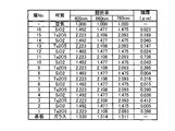
- 3 is a table showing a configuration of a dielectric multilayer film that forms convex portions of a diffractive member according to Example 1;
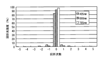
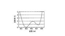
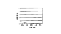
- 6 is a graph showing the intensity of diffracted light when laser light having wavelengths of 0.405 ⁇ m, 0.660 ⁇ m, and 0.785 ⁇ m is diffracted by the diffractive member according to Example 1. It is a graph which shows the wavelength dependence of the reflectance of the dielectric multilayer film which forms the convex part of the diffraction member concerning Example 1.
- FIG. 3 is a table showing a configuration of a dielectric multilayer film that forms convex portions of a diffractive member according to Example 1; 6 is a graph showing the intensity of diffracted light when laser light having wavelengths of 0.405 ⁇ m, 0.660 ⁇ m, and 0.785 ⁇ m is diffracted by the diffractive member according to Example 1.
- FIG. 6 is a graph showing the intensity of diffracted light when laser light having wavelengths of 0.405 ⁇ m, 0.660 ⁇ m, and 0.785 ⁇ m is diffracted by the diffractive member according to Example 1.
- 6 is a table showing a configuration of a dielectric multilayer film that forms convex portions of a diffractive member according to Example 2.
- 6 is a graph showing the intensity of diffracted light when laser light with wavelengths of 0.660 ⁇ m and 0.785 ⁇ m is diffracted by the diffractive member according to Example 2. It is a graph which shows the intensity
- FIG. 6 is a graph showing the intensity of diffracted light when laser light with wavelengths of 0.660 ⁇ m and 0.785 ⁇ m is diffracted by the diffractive member according to Example 2.
- FIG. 1 shows an example of an optical pickup optical system 1 according to an embodiment of the present invention.
- the optical pickup optical system 1 includes a laser unit 11 (light source), a grating element 12, a beam splitter 13, a collimator lens 14, a pickup lens 15, a detection system 16, and the like.
- CD17, DVD18, and BD19 will be described as examples of the optical disk. Note that the range of the optical disc to which the present invention is applied is not limited to the CD 17, the DVD 18, and the BD 19.
- the laser unit 11 includes a CD laser light source 111, a DVD laser light source 112BD, a laser light source 113 for BD, and the like.
- the wavelength of the laser light emitted from the CD laser light source 111, the wavelength of the laser light emitted from the DVD laser light source 112, and the wavelength of the laser light emitted from the BD laser light source 113 are different.
- the CD laser light source 111 emits laser light having a wavelength of 0.785 ⁇ m, which is used for recording / reproducing the CD 17.
- the DVD laser light source 112 emits a laser beam having a wavelength of 0.660 ⁇ m, which is a laser beam used for recording / reproducing the DVD 18.
- the BD laser light source 113 emits laser light having a wavelength of 0.405 ⁇ m, which is used for recording / reproducing the BD 19.
- a CD laser light source 111, a DVD laser light source 112, and a BD laser light source 113 are integrated into one package.
- the optical path of the laser beam emitted from the CD laser light source 111 is indicated by a broken line.
- the optical path of the laser light emitted from the DVD laser light source 112 is indicated by a dotted line.
- the optical path of the laser light emitted from the BD laser light source 113 is indicated by a one-dot chain line.
- the laser unit 11 may include two semiconductor laser light sources. Further, the laser unit 11 may be provided with three or more semiconductor laser light sources having different wavelengths.
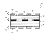
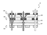
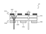
- FIG. 2 is a side view showing an example of the grating element 12 according to the embodiment of the present invention. Further, FIG. 3 shows a state of diffraction in the grating element 12.
- the grating element 12 includes a plurality of diffraction members 12A, 12B, and 12C.
- the diffractive member 12A has convex portions 12G and concave portions 12H arranged alternately on one surface of the transparent substrate 12D.
- the diffractive member 12B has convex portions 12I and concave portions 12J arranged alternately on one surface of the transparent substrate 12E.
- the diffractive member 12C has convex portions 12K and concave portions 12L arranged alternately on one surface of the transparent substrate 12F.
- the plurality of diffractive members 12A, 12B, and 12C are stacked in a direction substantially perpendicular to the transparent substrates 12D, 12E, and 12F. As shown in FIG. 3, the wavelengths of the laser beams diffracted by the plurality of diffraction members 12A, 12B, and 12C are different from each other. Further, each of the plurality of diffractive members 12A, 12B, and 12C diffracts the laser light and mainly generates 0th-order diffracted light, + 1st-order diffracted light, and ⁇ 1st-order diffracted light.
- a beam splitter 13 is provided on the optical path of the laser light emitted from the grating element 12.
- a collimator lens 14 is provided on the optical path of the laser light emitted from the beam splitter 13. The collimator lens 14 converts the laser light emitted from the laser unit 11 from divergent light to substantially parallel light.
- a pickup lens 15 is provided on the optical path of the laser light transmitted through the collimator lens 14.
- the pickup lens 15 has a function of condensing incident light on the information recording surfaces of the optical discs 17, 18, and 19 to near the diffraction limit. Specifically, the pickup lens 15 condenses the 0th-order diffracted light, the + 1st-order diffracted light, and the ⁇ 1st-order diffracted light generated in the grating element 12 on the optical discs 17, 18, and 19, respectively. Then, the 0th-order diffracted light forms signal reproduction light spots (hereinafter referred to as main spots) on the optical discs 17, 18, and 19.
- main spots signal reproduction light spots
- the ⁇ first-order diffracted light forms light spots (hereinafter referred to as sub-spots) for generating tracking signals on the optical discs 17, 18, and 19.
- the pickup lens 15 further has a function of guiding the laser beam reflected by the information recording surfaces of the optical discs 17, 18, 19 to the detection system 16. Further, at the time of focus servo and tracking servo, the pickup lens 15 is operated by an actuator (not shown).
- Laser light emitted from the laser unit 11 is diffracted by the grating element 12 and is emitted mainly as 0th-order diffracted light, + 1st-order diffracted light, and ⁇ 1st-order diffracted light.
- the 0th-order diffracted light, the + 1st-order diffracted light, and the ⁇ 1st-order diffracted light emitted from the grating element 12 pass through the beam splitter 13 and enter the collimator lens 14.
- the collimator lens 14 converts the 0th-order diffracted light, the + 1st-order diffracted light, and the ⁇ 1st-order diffracted light emitted from the laser unit 11 from divergent light into substantially parallel light.
- the pickup lens 15 focuses the 0th-order diffracted light, the + 1st-order diffracted light, and the ⁇ 1st-order diffracted light on the information recording surfaces of the optical discs 17, 18, and 19 to near the diffraction limit.
- the 0th-order diffracted light, the + 1st-order diffracted light, and the ⁇ 1st-order diffracted light reflected by the information recording surfaces of the optical discs 17, 18, and 19 are incident on the detection system 16 through the pickup lens 15 and detected.
- the detection system 16 detects the 0th-order diffracted light, the + 1st-order diffracted light, and the -1st-order diffracted light, and performs photoelectric conversion to generate a reproduction signal, a focus servo signal, a track servo signal, and the like.
- the grating element 12 used in the optical pickup optical system 1 according to the embodiment of the present invention will be described in detail.
- the grating element 12 includes a plurality of diffraction members 12A, 12B, and 12C.
- the diffractive member 12A has convex portions 12G and concave portions 12H arranged alternately on the exit surface of the transparent substrate 12D.
- convex portions 12G and concave portions 12H are periodically formed on the exit surface of the transparent substrate 12D of the diffractive member 12A.
- convex portions 12I and concave portions 12J are periodically formed on the exit surface of the transparent substrate 12E of the diffractive member 12B.
- convex portions 12K and concave portions 12L are periodically formed on the incident surface of the transparent substrate 12F of the diffractive member 12C.
- the plurality of diffractive members 12A, 12B, and 12C are bonded with an adhesive material so as to be stacked in a direction substantially perpendicular to the transparent substrates 12D, 12E, and 12F.
- the transparent substrates 12D, 12E, and 12F substrates formed of glass, quartz, resin, or the like can be used as the transparent substrates 12D, 12E, and 12F.
- the convex part 12G formed in the output surface of transparent substrate 12D and the convex part I formed in the output surface of transparent substrate 12E are formed of the dielectric multilayer film.
- the dielectric multilayer film is formed by laminating two or more kinds of dielectric films on the transparent substrates 12D and 12E in a direction substantially perpendicular to the transparent substrates 12D and 12E.
- the dielectric multilayer film is formed by alternately laminating the low refractive index material.
- a dielectric film can be formed using a vacuum evaporation method or a sputtering method.
- the ion assist vapor deposition method and ion beam sputtering method often used in optical multilayer films can suitably control the flatness and film thickness of the film. Therefore, it is more preferable to form a dielectric film using an ion assist vapor deposition method or an ion beam sputtering method.
- the recesses 12H of the transparent substrate 12D and the recesses 12J of the transparent substrate 12E are formed using a photolithography method, a dry etching method, and an ion milling method.
- a resist multilayer is formed on the transparent substrates 12D and 12E using a photolithography method, and then a dielectric multilayer film is formed. Thereafter, the recess 12H of the transparent substrate 12D and the recess 12J of the transparent substrate 12E may be formed by removing the resist.
- the convex portion 12K is formed on the emission surface of the transparent substrate 12F with an ultraviolet curable resin.
- the convex portion 12K and the concave portion 12L may be formed on the emission surface of the transparent substrate 12F by using a dry etching method or the like.
- the transparent substrate 12F may be injection-molded so that the emission surface of the transparent substrate 12F has a concavo-convex shape having convex portions 12K and concave portions 12L.
- arrows indicated by cross-hatching, arrows indicated by hatching, and white arrows indicate laser beams having different wavelengths.
- the laser beam indicated by the cross-hatching arrow is diffracted by the diffraction member 12C with a predetermined diffraction efficiency, and is not substantially diffracted by the diffraction members 12A and 12B.
- the laser beam indicated by the hatching arrow is diffracted by the diffraction member 12B with a predetermined diffraction efficiency, and is not substantially diffracted by the diffraction members 12A and 12C.
- the laser beam indicated by the white arrow is diffracted by the diffraction member 12A with a predetermined diffraction efficiency, and is not substantially diffracted by the diffraction members 12B and 12C. That is, the wavelengths of the laser beams diffracted by the plurality of diffraction members 12A, 12B, and 12C with a predetermined diffraction efficiency are different from each other.
- the predetermined diffraction efficiency is a diffraction efficiency that generates a predetermined amount of diffracted light.
- the predetermined amount is diffracted light whose spectral ratio is in the range of about 0.05 to 0.10 when the spectral ratio is (the intensity of diffracted light at a certain order / the intensity of 0th-order diffracted light). Of strength. Therefore, the wavelengths of the laser beams diffracted so that the plurality of diffraction members 12A, 12B, and 12C have a spectral ratio of about 0.05 to 0.10 are different.
- the spectral ratio is smaller than 0.05, the intensity of the sub-spot is reduced, and it is difficult to obtain a good tracking signal.
- the spectral ratio is greater than 0.10, the intensity of the main spot is reduced, which causes a reduction in the reproduction signal level. Therefore, it is preferable to diffract the laser light so that the spectral ratio is about 0.05 to 0.10.
- the plurality of diffraction members 12A, 12B, and 12C diffract the laser beam so that the spectral ratio is 0.05 to 0.10, respectively. And a good tracking signal can be obtained.
- the wavelengths of the laser beams diffracted by the plurality of diffraction members 12A, B, and C are different from each other. Therefore, the grating element 12 diffracts the laser beams emitted from the CD laser light source 111 and the DVD laser light source 112 BD laser light source 113 of the laser unit 11, respectively, so that the main spot on the CD 17, DVD 18, and BD 19 Subspots can be formed. Therefore, for example, an optical disc drive apparatus that reproduces CD17, DVD18, and BD19, which uses a laser unit in which a plurality of blue / red / infrared semiconductor lasers are integrated in one package as a light source.
- a grating element 12 can be mounted. In this case, the grating element 12 can form a main spot and a sub spot on the CD 17, DVD 18, and BD 19 independently from laser beams emitted from a plurality of blue / red / infrared semiconductor lasers.
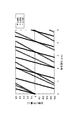
- FIG. 4 shows the relationship between the phase shift amount added to the laser beam and the grating depth (height of the convex portion) by the grating element formed of a single material.
- the grating element is a transparent substrate having an uneven shape on one surface.
- the horizontal axis indicates the grating depth ( ⁇ m)
- the vertical axis indicates the phase shift amount ( ⁇ ).
- Black circles indicate laser light with a wavelength of 0.405 ⁇ m
- white circles indicate laser light with a wavelength of 0.660 ⁇ m
- crosses indicate laser light with a wavelength of 0.785 ⁇ m.
- the refractive index of the single material is 1.492 at a wavelength of 0.405 ⁇ m, 1.477 at a wavelength of 0.660 ⁇ m, and 1.475 at a wavelength of 0.785 ⁇ m.
- a laser beam having a wavelength of 0.405 ⁇ m is usually used for recording / reproducing of the BD 19.
- a laser beam having a wavelength of 0.660 ⁇ m is normally used for recording / reproducing of the DVD 18.
- a laser beam having a wavelength of 0.785 ⁇ m is usually used for recording / reproducing of the CD 17.
- the grating element is a transparent substrate having an uneven shape on one surface, and is formed of a single material. Therefore, in order to selectively diffract a plurality of laser beams having different wavelengths by the grating element, the phase shift amount added to the laser light diffracted by the grating element is an appropriate value, and The grating depth needs to be set so that the amount of phase shift added to the laser light not diffracted by the grating element is about 0 ⁇ . As shown in FIG.
- the phase shift amount added to the laser light having a wavelength of 0.660 ⁇ m is added to the laser light having a wavelength of about 0.19 ⁇ , a wavelength of 0.405 ⁇ m, and a wavelength of 0.785 ⁇ m.
- the phase shift amount is about 0 ⁇ . Therefore, only a laser beam having a wavelength of 0.660 ⁇ m can be selectively diffracted by the grating element having a grating depth of about 1.65 ⁇ m.
- the phase shift amount added to the laser light having the wavelength of 0.405 ⁇ m and the wavelength of 0.660 ⁇ m is about 0 ⁇
- the phase shift amount added to the laser light having the wavelength of 0.785 ⁇ m is about 0 ⁇ . It becomes too large with about 0.5 ⁇ . Therefore, it is impossible to diffract a laser beam having a wavelength of 0.785 ⁇ m with a suitable diffraction efficiency. Further, from FIG.
- the grating depth is set such that an appropriate phase shift amount is added to the laser beam having a wavelength of 0.405 ⁇ m and the phase shift amount added to the laser beam having a wavelength of 0.660 ⁇ m and a wavelength of 0.785 ⁇ m is about 0 ⁇ .
- this does not exist in the practical range of the lattice depth (0 to 5 ⁇ m). Therefore, the grating element made of a single material cannot selectively diffract these three laser beams having different wavelengths.
- the convex portions 12G and 12I of at least one diffraction member 12A, 12B among the plurality of diffraction members 12A, 12B, 12C are formed of a dielectric multilayer film.
- a convex portion in a diffraction member that diffracts laser light having a wavelength of 0.405 ⁇ m and laser light having a wavelength of 0.785 ⁇ m with a predetermined diffraction efficiency is formed of a dielectric multilayer film.
- the convex portions 12G, 12I, and 12K of all the diffractive members 12A, 12B, and 12C may be formed of a dielectric multilayer film.
- the wavelength of the laser light transmitted through the dielectric multilayer film is ⁇
- the refractive index of the medium in the space adjacent to the dielectric multilayer film is n 0
- the refractive index of the high refractive index material constituting the dielectric multilayer film is n H
- the dielectric When the refractive index of the low refractive index material constituting the body multilayer film is n L , the total film thickness of the high refractive index material is d H , and the total film thickness of the low refractive index material is d L , the dielectric multilayer A phase shift amount ⁇ (unit: wavelength ⁇ ) added to the laser light transmitted through the film is expressed by the following equation (8).
- the height of the convex portions 12G and 12I (the height of the dielectric multilayer film) capable of diffracting only one laser beam of a plurality of laser beams having different wavelengths with a predetermined diffraction efficiency is set.
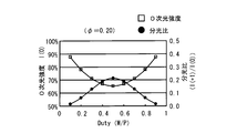
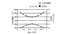
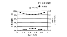
- FIG. 6 show the convex portion of the grating element with respect to the pitch of the grating structure of the diffractive member, and the intensity and spectral ratio (the intensity of the first-order diffracted light / the intensity of the zero-order diffracted light) of the grating element. Width ratio) dependence.
- the grating element according to FIGS. 5 to 8 is a transparent substrate having a concavo-convex shape on one surface, and is formed of a single material.
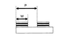
- Duty is the ratio of the width W of the convex portion to the pitch P (the sum of the width of the convex portion and the width of the concave portion) of the grating structure of the diffractive member.
- the phase is a periodic function
- the intensity of the diffracted light was calculated. Specifically, each coefficient of the Fourier series expansion of the phase function was obtained, and the square of the absolute value of each coefficient was obtained.
- the spectral ratio (I (+1) / I (0)) is preferably in the range of 0.05 to 0.10. Therefore, in the grating element 12 according to the present embodiment, when the phase shift amount added to the laser light to be diffracted is ⁇ D and the phase shift amount added to the laser light not substantially diffracted is ⁇ ND , the following ( 3) so as to satisfy equation and (4), sets the d H and d L.
- the spectral ratio (I (+1) / I (0)) can be in the range of 0.05 to 0.10 at the diffracted wavelength. As a result, the reproduction signal level can be prevented from being lowered and a good tracking signal can be obtained. Further, by satisfying the expression (4), the intensity I (0) of the 0th-order diffracted light of the laser light that is not substantially diffracted becomes larger than 90%. Thereby, the light utilization efficiency of the 0th-order diffracted light of the laser light which is not substantially diffracted can be improved.
- the dielectric multilayer film according to the present embodiment is formed by alternately laminating dielectric films formed from a high refractive index material and dielectric films formed from a low refractive index material.
- the dielectric multilayer film according to the present embodiment has a function of preventing the laser light incident on the dielectric multilayer film from being reflected by the dielectric multilayer film.
- the number of layers of the dielectric multilayer film according to the present embodiment is determined so that the reflectance with which the laser light incident on the dielectric multilayer film is reflected by the dielectric multilayer film is low.
- the reflectance is the ratio of the intensity of the laser light reflected on the dielectric multilayer film to the intensity of the laser light incident on the dielectric multilayer film.
- the recesses 12H, 12J, and 12L are made of the same material as the transparent substrates 12D, 12E, and 12F. Therefore, in the recesses 12H, 12J, and 12L, the laser light incident on the grating element 12 is reflected according to the refractive indexes of the transparent substrates 12D, 12E, and 12F. Therefore, it is preferable that the following expression (7) is satisfied, where P is the pitch of the grating structure of the diffractive members 12A and 12B, and W is the width of the convex portions 12G and 12I.
- variety of the convex parts 12G and 12I which have an antireflection function can be made larger than the width
- the plot shape of the intensity I (0) of the 0th-order diffracted light and the plot shape of the spectral ratio (I (+1) / I (0)) are 0 ⁇ W / P ⁇ 0. .5 and 0.5 ⁇ W / P ⁇ 1 are left and right contrasts. Therefore, the intensity I (0) and spectral ratio (I (+1) / I (0)) of the 0th-order diffracted light obtained in the range of 0 ⁇ W / P ⁇ 0.5 and 0.5 ⁇ W / P ⁇ 1
- the intensity I (0) and the spectral ratio (I (+1) / I (0)) of the 0th-order diffracted light obtained in the range are substantially the same. Therefore, in the present embodiment, the duty is set within the range of 0.5 ⁇ W / P ⁇ 1.0, which can further suppress the reflection of incident light.
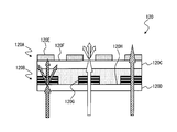
- the grating element 120 includes a plurality of diffraction members 120A and 120B.
- the diffractive member 120A has convex portions 120E and concave portions 120F arranged alternately on the exit surface of the transparent substrate 120C.
- convex portions 120E and concave portions 120F are periodically formed on the exit surface of the transparent substrate 120C of the diffractive member 120A.
- convex portions 120G and concave portions 120H are periodically formed on the exit surface of the transparent substrate 120D of the diffractive member 120B.
- the plurality of diffractive members 120A and 120B are bonded together with an adhesive material so as to be stacked in a direction substantially perpendicular to the transparent substrates 120C and 120D. Specifically, the entrance surface of the transparent substrate 120C and the exit surface of the transparent substrate 120D are bonded together with an adhesive material. Since the materials of the transparent substrates 120C and 120D are the same as those of the transparent substrates 12D, 12E, and 12F, description thereof is omitted.
- the convex portion 120G formed on the emission surface of the transparent substrate 120D is formed of a dielectric multilayer film. Since the material and manufacturing method of the dielectric multilayer film are the same as those of the grating element 12, the description thereof is omitted. Moreover, since the formation method of the recessed part 120H of transparent substrate 120D is the same as that of the recessed part 12H and the recessed part 12J, the description is abbreviate
- an arrow indicated by hatching, a white arrow, and an arrow indicated by cross hatching indicate laser beams having different wavelengths.
- the laser beam indicated by the hatching arrow is diffracted by the diffraction member 120B with a predetermined diffraction efficiency, and is not substantially diffracted by the diffraction member 120A.
- the laser beam indicated by the white arrow is diffracted by the diffraction member 120A with a predetermined diffraction efficiency, and is not substantially diffracted by the diffraction member 120B.
- the laser light indicated by the cross-hatched arrows is not substantially diffracted by the diffraction members 120A and 120B.
- the wavelengths of the laser beams diffracted by the plurality of diffractive members 120A and 120B with a predetermined diffraction efficiency are different. Further, the laser beam indicated by the cross-hatched arrow passes through the grating element 120 without being substantially diffracted.
- the spectral ratio (I (+1) / I (0)) is preferably in the range of 0.05 to 0.10. Therefore, in the grating element 120 according to the present embodiment, when the phase shift amount added to the laser light to be diffracted is ⁇ D , and the phase shift amount added to the laser light not substantially diffracted is ⁇ ND , the following ( 3) so as to satisfy equation and (4), sets the d H and d L. 0.10 ⁇
- the reproduction signal level can be prevented from being lowered and a good tracking signal can be obtained.
- the intensity I (0) of the 0th-order diffracted light of the laser light that is not substantially diffracted becomes larger than 90%.
- the diffractive member 120A moves the laser beam indicated by the white arrow to the kth order (k ⁇ 0) with higher diffraction efficiency than the laser beam indicated by the hatched arrow and the laser beam indicated by the cross-hatched arrow. Diffraction.
- the diffractive member 120A does not substantially diffract the laser light indicated by the hatching arrow and the laser light indicated by the cross-hatching arrow.
- the laser beam indicated by the hatching arrow and the laser beam indicated by the cross-hatching arrow are not substantially diffracted means that the laser beam indicated by the hatching arrow and the zero-order diffracted light of the laser beam indicated by the cross-hatching arrow This means that the laser beam indicated by the hatching arrow and the laser beam indicated by the cross-hatching arrow are slightly diffracted so that the intensity I (0) of the laser beam becomes greater than 90% of the intensity of the incident light.
- the diffractive member 120B diffracts the laser beam indicated by the hatched arrow to the kth order (k ⁇ 0) with higher diffraction efficiency than the laser beam indicated by the white arrow and the laser beam indicated by the cross-hatched arrow.
- the diffractive member 120B does not substantially diffract the laser beam indicated by the white arrow and the laser beam indicated by the cross-hatched arrow.
- “the laser light indicated by the white arrow and the laser light indicated by the cross-hatching arrow are not substantially diffracted” means that the laser light indicated by the white arrow and the laser light indicated by the cross-hatching arrow are zero. This means that the laser beam indicated by the white arrow and the laser beam indicated by the cross-hatched arrow are slightly diffracted so that the intensity I (0) of the next diffracted light is greater than 90% of the intensity of the incident light.
- the tracking method differs depending on the wavelength of the laser beam (depending on the type of the optical disk), and a method of splitting the laser beam into three beams and a method of not splitting the laser beam are mixed. It can be used for such an optical disc drive apparatus.
- the grating element in an optical disk drive apparatus that reproduces CD17, DVD18, and BD19 and uses a laser unit in which a plurality of blue / red / infrared semiconductor lasers are integrated in one package as a light source. 12 can be mounted.
- the sub spot is formed from blue laser light.
- the main spot and the sub spot can be formed on the CD 17 and the DVD 18 independently from the red laser beam and the infrared laser beam.
- the blue laser light is not substantially diffracted by the grating element 120. Therefore, it is possible to suppress a reduction in the light use efficiency of the 0th-order diffracted light.
- FIG. 11 shows a grating element 121 according to another example of the present embodiment.
- the grating element 121 is applied to an optical disk drive device that uses two laser beams having different wavelengths.
- the grating element 121 includes a plurality of diffraction members 121A and 121B.
- the diffraction member 121A has convex portions 121E and concave portions 121F arranged alternately on the exit surface of the transparent substrate 121C.
- convex portions 121E and concave portions 121F are periodically formed on the exit surface of the transparent substrate 121C of the diffractive member 121A.
- convex portions 121G and concave portions 121H are periodically formed on the incident surface of the transparent substrate 121D of the diffractive member 121B.
- the plurality of diffractive members 121A and 121B are bonded with an adhesive material so as to be stacked in a direction substantially perpendicular to the transparent substrates 121C and 121D.
- the entrance surface of the transparent substrate 121C and the exit surface of the transparent substrate 121D are bonded together with an adhesive material. Since the materials of the transparent substrates 121C and 121D are the same as those of the transparent substrates 12D, 12E, and 12F, description thereof is omitted.
- the convex portion 121E formed on the emission surface of the transparent substrate 121C is formed of a dielectric multilayer film. Since the material and manufacturing method of the dielectric multilayer film are the same as those of the dielectric multilayer film of the grating element 12, the description thereof is omitted. Moreover, since the formation method of the recessed part 121F of the transparent substrate 121C is the same as that of the recessed part 12H and the recessed part 12J, the description is abbreviate
- hatched arrows and white arrows indicate laser beams having different wavelengths.
- the laser beam indicated by the hatching arrow is diffracted by the diffraction member 120B with a predetermined diffraction efficiency, and is not substantially diffracted by the diffraction member 120A.
- the laser beam indicated by the white arrow is diffracted by the diffraction member 120A with a predetermined diffraction efficiency, and is not substantially diffracted by the diffraction member 120B. That is, the wavelengths of the laser beams diffracted by the plurality of diffractive members 120A and 120B with a predetermined diffraction efficiency are different.
- the grating element 120 having such a function is, for example, an optical disc drive device that reproduces a CD 17 and a DVD 18, and uses a laser unit in which a plurality of red / infrared semiconductor lasers are integrated in one package as a light source. It can be used for an optical disk drive device.
- a main spot and a sub spot can be formed on the CD 17 and the DVD 18 independently from laser light emitted from a plurality of red / infrared semiconductor lasers.
- the spectral ratio (I (+1) / I (0)) is preferably in the range of 0.05 to 0.10. Therefore, in the grating element 121 according to the present embodiment, when the phase shift amount added to the laser beam to be diffracted is ⁇ D and the phase shift amount added to the laser beam not substantially diffracted is ⁇ ND , the following ( 3) so as to satisfy equation and (4), sets the d H and d L. 0.10 ⁇
- the reproduction signal level can be prevented from being lowered and a good tracking signal can be obtained.
- the intensity I (0) of the 0th-order diffracted light of the laser light that is not substantially diffracted becomes larger than 90%.
- the light utilization efficiency of the 0th-order diffracted light of the laser light which is not substantially diffracted can be improved.
- the diffractive member 121A diffracts the laser beam indicated by the white arrow to the kth order (k ⁇ 0) with higher diffraction efficiency than the laser beam indicated by the hatched arrow. Further, the diffractive member 121A does not substantially diffract the laser beam indicated by the hatched arrow.
- the laser beam indicated by the hatching arrow is not substantially diffracted” means that the intensity I (0) of the zero-order diffracted light of the laser beam indicated by the hatching arrow is greater than 90% of the incident light intensity. Furthermore, it means that the laser beam indicated by the hatching arrow is slightly diffracted. Similarly, the diffractive member 121B diffracts the laser beam indicated by the hatched arrow to the kth order (k ⁇ 0) with higher diffraction efficiency than the laser beam indicated by the hollow arrow. Furthermore, the diffractive member 121B does not substantially diffract the laser beam indicated by the white arrow.
- the laser beam indicated by the white arrow is not substantially diffracted” means that the intensity I (0) of the zero-order diffracted light of the laser beam indicated by the white arrow is greater than 90% of the intensity of the incident light. This means that the laser beam indicated by the white arrow is slightly diffracted.
- the grating element 121 does not diffract the wavelength of the laser light to be diffracted at a predetermined diffraction efficiency lambda D, substantially
- the wavelength of the laser beam is ⁇ ND
- the refractive index at the wavelength ⁇ ND of the high refractive index material is n HND
- the refractive index at the wavelength ⁇ ND of the low refractive index material is n LND
- Patent Document 1 when a laser beam having a wavelength different from the wavelength of the laser beam diffracting the grating element is transmitted, the phase difference between the light beam transmitted between the grooves and the light beam transmitted through the groove is 2 ⁇ (the laser beam). It is described that the depth of the groove is set so as to be equal to 1 times the wavelength of. The depth of the groove varies depending on the refractive index of the grating element. However, in Patent Document 1, approximate calculation based on the scalar diffraction theory shown in the following equations (1) and (2) is performed.
- n 1 is the refractive index of the grating element
- d 1 is the depth of the groove
- ⁇ 1 is a wavelength different from the wavelength of the laser light diffracted by the grating element (the wavelength of the laser light that is not substantially diffracted).
- ⁇ 1 (0) is the light utilization efficiency of the 0th-order diffracted light of the laser light having the wavelength ⁇ 1 .
- the diffraction efficiency changes depending on the depth of the groove even if the phase difference between the light transmitted through the grooves and the light transmitted through the grooves is 2 ⁇ . To do. That is, in the exact calculation based on the vector diffraction theory using the electromagnetic field analysis, even if the expression (1) is satisfied, the expression (2) cannot be satisfied, and the light use efficiency of the 0th-order diffracted light does not reach 100%. This decrease in light utilization efficiency is particularly noticeable in a grating element having a narrow pitch of the diffractive structure.
- the light utilization efficiency of the 0th-order diffracted light calculated by the exact calculation can be improved. That is, by determining the height of the convex portion so as to satisfy the expressions (5) and (6), the light use efficiency of the 0th-order diffracted light calculated by the exact calculation can be improved.
- the graph of FIG. 12 shows the relationship between the light utilization efficiency of the 0th-order diffracted light of the laser light having a wavelength of 0.785 ⁇ m and the grating depth.
- the grating element used in FIG. 12 is a transparent substrate having an uneven shape on one surface, and is formed from a single material.
- the refractive index of the grating element is 1.500.
- the vertical axis represents the intensity of the 0th-order diffracted light
- the horizontal axis represents the grating depth (the height of the convex portion). Further, the intensity of the 0th-order diffracted light was expressed with the intensity of the incident light as 100%.
- the intensity of the diffracted light was obtained by exact calculation by the finite difference time domain method (FDTD method).
- FDTD method finite difference time domain method
- white triangle marks indicate data when the pitch of the lattice structure is 50 ⁇ m
- white square marks indicate data when the pitch of the lattice structure is 30 ⁇ m
- black circles indicate the lattice structure.
- the data when the pitch is 10 ⁇ m is shown.
- the intensities of the 0th-order diffracted light at a grating depth of 1.57 ⁇ m, 4.71 ⁇ m, and 9.42 ⁇ m are plotted in FIG.
- the grating depths of 1.57 ⁇ m, 4.71 ⁇ m, and 9.42 ⁇ m are the depths at which phase differences of 2 ⁇ , 6 ⁇ , and 12 ⁇ are generated in laser light having a wavelength of 0.785 ⁇ m, respectively.
- the grating depths of 1.57 ⁇ m, 4.71 ⁇ m, and 9.42 ⁇ m are depths that generate a phase difference that is an integral multiple of the wavelength in the laser light having a wavelength of 0.785 ⁇ m. That is, the grating depths of 1.57 ⁇ m, 4.71 ⁇ m, and 9.42 ⁇ m do not cause a phase shift in the laser light having a wavelength of 0.785 ⁇ m.
- the intensity of the 0th-order diffracted light is 100% in the approximate calculation based on the scalar diffraction theory.
- the intensity of the next diffracted light does not reach 100%.
- the decrease in the intensity of the 0th-order diffracted light becomes more conspicuous as the pitch of the grating structure is narrower.
- the grating depth is made shallow (the height of the convex part is lowered), and the wavelength of the laser light that is not diffracted is reduced. What is necessary is just to make it the depth which generates the phase difference of integral multiple. Equations (5) and (6) are used to reduce the height of the convex portion formed by the dielectric multilayer film as much as possible and to generate a phase difference that is an integral multiple of the wavelength of laser light that is not diffracted.
- the light utilization efficiency of the 0th-order diffracted light calculated by the exact calculation can be improved. That is, by determining the height of the convex portion so as to satisfy the expressions (5) and (6), the light use efficiency of the 0th-order diffracted light calculated by the exact calculation can be improved.
- the dielectric multilayer film includes dielectric films formed of a high refractive index material and dielectric films formed of a low refractive index material alternately. It is formed by stacking.
- the dielectric multilayer films of the grating element 120 and the grating element 121 have a function of preventing the laser light incident on the dielectric multilayer film from being reflected by the dielectric multilayer film.
- the number of layers of the dielectric multilayer film is such that the reflectivity at which the laser light incident on the dielectric multilayer film is reflected by the dielectric multilayer film.
- the concave / convex shape of one diffraction member is formed on one surface of the transparent substrate, and the concave / convex shape of another diffraction member is formed on the other surface of the transparent substrate, so that two types of diffraction members are integrated. May be formed. Thereby, the process of bonding a diffraction member can be reduced, and cost can be reduced.
- Example 1 As Example 1, an example of the grating element 12 shown in FIG. There are three types of laser beams that pass through the grating element 12. The wavelengths of the three types of laser light are 0.405 ⁇ m, 0.660 ⁇ m, and 0.785 ⁇ m, respectively.
- the convex portion 12G of the diffractive member 12A and the convex portion 12I of the diffractive member 12B were formed of a dielectric multilayer film.
- the diffractive member 12C and the convex portion 12K of the diffractive member 12C were integrally formed of the same material.
- the diffractive member 12C and the convex portion 12K were made of quartz.
- the diffraction wavelength of the diffractive member 12A is 0.405 ⁇ m, and the non-diffractive wavelengths are 0.660 ⁇ m and 0.785 ⁇ m.
- the pitch (P) of the grating structure of the diffractive member 12A is 50 ⁇ m, and Duty (W / P) is 0.700.
- the height (lattice depth: d) of the convex portion 12G is 3.672 ⁇ m.
- the refractive index of the transparent substrate 12D of the diffractive member 12A is 1.530 at a wavelength of 0.405 ⁇ m, 1.514 at a wavelength of 0.660 ⁇ m, and 1.511 at a wavelength of 0.785 ⁇ m.
- the refractive index of the medium in the space adjacent to the convex portion 12G is 1.000.
- the diffraction wavelength of the diffractive member 12B is 0.785 ⁇ m, and the non-diffracted wavelengths are 0.405 ⁇ m and 0.660 ⁇ m.
- the pitch (P) of the grating structure of the diffractive member 12B is 60 ⁇ m, and Duty (W / P) is 0.583.
- the height (lattice depth: d) of the convex portion 12I is 1.300 ⁇ m.
- the refractive index of the transparent substrate 12E of the diffractive member 12B is 1.530 at a wavelength of 0.405 ⁇ m, 1.514 at a wavelength of 0.660 ⁇ m, and 1.511 at a wavelength of 0.785 ⁇ m.
- the medium in the space adjacent to the convex portion 12I is an adhesive material, and the refractive index of the adhesive material is 1.400 at a wavelength of 0.405 ⁇ m, 1.385 at a wavelength of 0.660 ⁇ m, and 1.382 at a wavelength of 0.785 ⁇ m. is there.
- the diffraction wavelength of the diffractive member 12C is 0.660 ⁇ m, and the non-diffractive wavelengths are 0.405 ⁇ m and 0.785 ⁇ m.
- the pitch (P) of the grating structure of the diffractive member 12C is 50 ⁇ m, and Duty (W / P) is 0.500. Further, the height (lattice depth: d) of the convex portion 12K is 1.645 ⁇ m.
- the refractive index of the transparent substrate 12F of the diffractive member 12C is 1.492 at a wavelength of 0.405 ⁇ m, 1.477 at a wavelength of 0.660 ⁇ m, and 1.475 at a wavelength of 0.785 ⁇ m.
- the refractive index of the convex portion 12K is 1.492 at a wavelength of 0.405 ⁇ m, 1.477 at a wavelength of 0.660 ⁇ m, and 1.475 at a wavelength of 0.785 ⁇ m. Further, since the medium in the space adjacent to the convex portion 12K is air, the refractive index of the medium in the space adjacent to the convex portion 12K is 1.000.
- the table shown in FIG. 13 shows the configuration of the dielectric multilayer film that forms the convex portion 12G of the diffractive member 12A.
- Ta 2 O 5 was used as the high refractive index material, and SiO 2 was used as the low refractive index material.
- the number of layers of the dielectric multilayer film is 16.
- the total thickness d AH of Ta 2 O 5 is 3.483 ⁇ m
- the total thickness d AL of SiO 2 is 0.189 ⁇ m
- the height (lattice depth) d A of the convex portion 12G is 3.672 ⁇ m. is there.
- the phase shift amount ⁇ 405 added to the laser beam having a wavelength of 0.405 ⁇ m by the diffractive member 12A is ⁇ 0.2498 ( ⁇ ), which satisfies the expression (3).
- the phase shift amounts ⁇ 660 and ⁇ 785 added to the laser beam having a wavelength of 0.660 ⁇ m and the laser beam having a wavelength of 0.785 ⁇ m by the diffraction member 12A are ⁇ 0.0170 ( ⁇ ) and ⁇ 0.0367 ( ⁇ ), respectively. Yes, the formula (4) is satisfied.
- FIG. 14 shows the intensity of diffracted light when laser light having wavelengths of 0.405 ⁇ m, 0.660 ⁇ m, and 0.785 ⁇ m is diffracted by the diffractive member 12A.
- the horizontal axis indicates the diffraction order, and the vertical axis indicates the intensity of the diffracted light.
- a bar graph indicated by cross hatching indicates the intensity of diffracted light of laser light having a wavelength of 0.405 ⁇ m.
- a bar graph indicated by hatching indicates the intensity of diffracted light of laser light having a wavelength of 0.660 ⁇ m. Further, in the graph of FIG.
- a white bar graph indicates the intensity of the diffracted light of the laser light having a wavelength of 0.785 ⁇ m. Further, the intensity of the diffracted light was obtained by exact calculation by the finite difference time domain method (FDTD method).
- FIG. 14 shows the intensity of diffracted light of each diffraction order when the intensity of incident light is 100%.
- the spectral ratio ( ⁇ 1st order diffracted light intensity / 0th order diffracted light intensity) of laser light having a wavelength of 0.405 ⁇ m is 1 / 17.2, and is in the range of 0.05 to 0.1. It has become. Further, the intensities of the 0th-order diffracted light of the laser beams having wavelengths of 0.660 ⁇ m and 0.785 ⁇ m were 92.4% and 97.0%, respectively. Therefore, the diffractive member 12A according to the first embodiment can diffract laser light having a wavelength of 0.405 ⁇ m to be diffracted with a suitable spectral ratio. In addition, the diffractive member 12A according to the first embodiment can transmit laser light having wavelengths of 0.660 ⁇ m and 0.785 ⁇ m that should not be diffracted substantially without diffracting.
- the horizontal axis represents wavelength (nm)
- the vertical axis represents reflectance (%).
- the reflectance is the ratio of the intensity of the laser light reflected on the dielectric multilayer film to the intensity of the laser light incident on the dielectric multilayer film.
- the reflectances at wavelengths of 0.405 ⁇ m, 0.660 ⁇ m, and 0.785 ⁇ m are 2% or less. Therefore, the dielectric multilayer film of the diffractive member 12A also has antireflection performance.
- the duty of the diffractive member 12A is 0.700, and the proportion of the convex portions 12G on the surface of the diffractive member 12A can be increased. Thereby, reflection of the laser beam incident on the diffractive member 12A can be effectively suppressed. Therefore, it is not necessary to apply an antireflection film to the diffractive member 12A.
- An antireflection film may be separately formed on the surface of the diffractive member 12A to further improve the antireflection performance.
- the table shown in FIG. 16 shows the configuration of the dielectric multilayer film that forms the convex portion 12I of the diffractive member 12B.
- Ta 2 O 5 was used as the high refractive index material
- SiO 2 was used as the low refractive index material.
- the number of dielectric multilayer films is twelve.
- Total thickness of the Ta 2 O 5 d BH are 0.900Myuemu
- sum d BL thickness of SiO 2 is 0.400Myuemu
- the height of the convex portions 12I (grating depth) d B is 1.300 ⁇ m is there.
- phase shift amount ⁇ 785 added to the laser beam having a wavelength of 0.785 ⁇ m by the diffractive member 12B is ⁇ 0.137 ( ⁇ ), which satisfies the expression (3).
- phase shift amounts ⁇ 405 and ⁇ 660 added to the laser beam having a wavelength of 0.405 ⁇ m and the laser beam having a wavelength of 0.660 ⁇ m by the diffraction member 12B are ⁇ 0.079 ( ⁇ ) and +0.042 ( ⁇ ), respectively. , (4) is satisfied.
- FIG. 17 shows the intensity of diffracted light when laser light having wavelengths of 0.405 ⁇ m, 0.660 ⁇ m, and 0.785 ⁇ m is diffracted by the diffractive member 12B.
- the horizontal axis represents the diffraction order
- the vertical axis represents the intensity of the diffracted light.
- a bar graph indicated by cross hatching indicates the intensity of diffracted light of laser light having a wavelength of 0.405 ⁇ m.
- the bar graph indicated by hatching indicates the intensity of the diffracted light of the laser light having a wavelength of 0.660 ⁇ m.
- the graph of FIG. 17 shows the intensity of diffracted light when laser light having wavelengths of 0.405 ⁇ m, 0.660 ⁇ m, and 0.785 ⁇ m is diffracted by the diffractive member 12B.
- the horizontal axis represents the diffraction order
- the vertical axis represents the intensity of the diffracted light.
- a bar graph indicated by cross hatching indicates the intensity of diffracted
- the bar graph shown in white indicates the intensity of the diffracted light of the laser light having a wavelength of 0.785 ⁇ m. Further, the intensity of the diffracted light was obtained by exact calculation by the finite difference time domain method (FDTD method).
- FIG. 17 shows the intensity of diffracted light of each diffraction order when the intensity of incident light is 100%.
- the spectral ratio ( ⁇ 1st order diffracted light intensity / 0th order diffracted light intensity) of laser light having a wavelength of 0.785 ⁇ m is 1 / 11.6, and is in the range of 0.05 to 0.1. It has become. Further, the intensities of the 0th-order diffracted light of the laser beams having wavelengths of 0.405 ⁇ m and 0.660 ⁇ m were 97.7% and 94.9%, respectively. Therefore, the diffractive member 12B according to the first embodiment can diffract laser light having a wavelength of 0.785 ⁇ m to be diffracted with a suitable spectral ratio. In addition, the diffractive member 12B according to the first embodiment can transmit laser beams having wavelengths of 0.405 ⁇ m and 0.660 ⁇ m that should not be diffracted substantially without diffracting.
- the horizontal axis represents wavelength (nm)
- the vertical axis represents reflectance (%).
- the reflectance is the ratio of the intensity of the laser light reflected on the dielectric multilayer film to the intensity of the laser light incident on the dielectric multilayer film.
- the reflectance at wavelengths of 0.405 ⁇ m, 0.660 ⁇ m, and 0.785 ⁇ m is 1% or less. Therefore, the dielectric multilayer film of the diffractive member 12B also has antireflection performance.
- the duty of the diffractive member 12B is 0.583, and the proportion of the convex portion 12I on the surface of the diffractive member 12B can be increased. Thereby, reflection of the laser beam incident on the diffractive member 12B can be effectively suppressed. Therefore, it is not necessary to apply an antireflection film to the diffractive member 12B.
- An antireflection film may be separately formed on the surface of the diffractive member 12B to further improve the antireflection performance.
- the diffractive member 12C is formed from one type of material. Therefore, if the refractive index of the diffractive member 12C is n, the refractive index of the medium in the space adjacent to the convex portion 12K is n 0 , the height (grating depth) of the convex portion 12K is d, and the wavelength of the laser light is ⁇ ,
- the phase shift amount ⁇ added to the laser beam having the wavelength ⁇ by the diffractive member 12C is expressed by the following equation (9).
- phase shift amount ⁇ 660 added to the laser beam having a wavelength of 0.660 ⁇ m by the diffractive member 12C is +0.189 ( ⁇ ), which satisfies the expression (3).
- phase shift amounts ⁇ 405 and ⁇ 785 added to the laser beam having a wavelength of 0.405 ⁇ m and the laser beam having a wavelength of 0.785 ⁇ m by the diffractive member 12C are ⁇ 0.002 ( ⁇ ) and ⁇ 0.005 ( ⁇ ), respectively. Yes, the formula (4) is satisfied.
- FIG. 19 shows the intensity of diffracted light when laser light having wavelengths of 0.405 ⁇ m, 0.660 ⁇ m, and 0.785 ⁇ m is diffracted by the diffractive member 12C.
- the horizontal axis represents the diffraction order, and the vertical axis represents the intensity of the diffracted light.
- a bar graph indicated by cross hatching indicates the intensity of diffracted light of laser light having a wavelength of 0.405 ⁇ m.
- a bar graph indicated by hatching indicates the intensity of diffracted light of laser light having a wavelength of 0.660 ⁇ m. Further, in the graph of FIG.
- FIG. 19 shows the intensity of diffracted light of each diffraction order when the intensity of incident light is 100%.
- the spectral ratio ( ⁇ 1st order diffracted light intensity / 0th order diffracted light intensity) of laser light having a wavelength of 0.660 ⁇ m is 1 / 14.3, and is in the range of 0.05 to 0.1. It has become.
- the intensities of the 0th-order diffracted light of the laser beams having wavelengths of 0.405 ⁇ m and 0.785 ⁇ m were 97.1% and 96.9%, respectively. Therefore, the diffractive member 12C according to the first embodiment can diffract laser light having a wavelength of 0.660 ⁇ m to be diffracted with a suitable spectral ratio.
- the diffractive member 12C according to the first example can transmit laser beams having wavelengths of 0.405 ⁇ m and 0.785 ⁇ m that should not be diffracted substantially without diffracting.
- it when it consists of one type of material like the diffraction member 12C, it is preferable to form an antireflection film on the surface of the diffraction member 12C. Then, as shown in FIG. 1, by attaching the diffractive members 12A, 12B, and 12C according to Example 1, laser beams having wavelengths of 0.405 ⁇ m, 0.660 ⁇ m, and 0.785 ⁇ m can be independently obtained with suitable diffraction efficiency. Thus, the grating element 12 that can be diffracted in the same manner is obtained.
- Example 2 As Example 2, an example of the grating element 121 shown in FIG. 11 is shown. There are two types of laser beams that pass through the grating element 121. The wavelengths of the two types of laser light are 0.660 ⁇ m and 0.785 ⁇ m, respectively. Further, the convex portion 121E of the diffractive member 121A is formed of a dielectric multilayer film. Moreover, the convex part 121G of the diffractive member 121B was formed of an acrylic resin.
- the diffraction wavelength of the diffractive member 121A is 0.660 ⁇ m, and the non-diffractive wavelength is 0.785 ⁇ m.
- the pitch (P) of the grating structure of the diffractive member 121A is 15 ⁇ m, and the Duty (W / P) is 0.800.
- the height (lattice depth: d) of the convex portion 121E is 0.760 ⁇ m.
- the refractive index of the transparent substrate 121C of the diffractive member 121A is 1.514 at a wavelength of 0.660 ⁇ m and 1.511 at a wavelength of 0.785 ⁇ m.
- the refractive index of the medium in the space adjacent to the convex portion 121E is 1.000.
- the diffraction wavelength of the diffractive member 121B is 0.785 ⁇ m, and the non-diffractive wavelength is 0.660 ⁇ m.
- the pitch (P) of the grating structure of the diffractive member 121B is 35 ⁇ m, and the Duty (W / P) is 0.24.
- the height (lattice depth: d) of the convex portion 121G is 1.320 ⁇ m.
- the refractive index of the transparent substrate 121D of the diffractive member 121B is 1.514 at a wavelength of 0.660 ⁇ m and 1.511 at a wavelength of 0.785 ⁇ m.
- the refractive index of the convex 121G is 1.500 at a wavelength of 0.660 ⁇ m and 1.497 at a wavelength of 0.785 ⁇ m. Further, since the medium in the space adjacent to the convex portion 121G is air, the refractive index of the medium in the space adjacent to the convex portion 121G is 1.000.
- the table shown in FIG. 20 shows the configuration of the dielectric multilayer film that forms the convex portion 121E of the diffractive member 121A.
- Ta 2 O 5 was used as the high refractive index material, and SiO 2 was used as the low refractive index material.
- the number of layers of the dielectric multilayer film is seven.
- the total film thickness d FH of Ta 2 O 5 is 0.640 ⁇ m
- the total film thickness d FL of SiO 2 is 0.120 ⁇ m
- the height (lattice depth) d F of the convex portion 121E is 0.760 ⁇ m. is there.
- ⁇ ND 0.785 ⁇ m
- n HND 2.093
- n LND 1.475
- n 0ND 1.000.
- L 0.180 ⁇ m
- d FH of Ta 2 O 5 and the total film thickness d FL of SiO 2 satisfy the expressions (5) and (6).
- phase shift amount ⁇ 660 added to the laser beam having a wavelength of 0.660 ⁇ m by the diffractive member 121A is +0.161 ( ⁇ ), which satisfies the expression (3).
- phase shift amount ⁇ 785 added to the laser beam having a wavelength of 0.785 ⁇ m by the diffractive member 121A is ⁇ 0.036 ( ⁇ ), which satisfies the expression (4).
- FIG. 21 shows the intensity of diffracted light when laser light having wavelengths of 0.660 ⁇ m and 0.785 ⁇ m is diffracted by the diffractive member 121A.
- the horizontal axis indicates the diffraction order
- the vertical axis indicates the intensity of the diffracted light.
- a bar graph indicated by hatching indicates the intensity of diffracted light of laser light having a wavelength of 0.660 ⁇ m.
- the bar graph shown in white indicates the intensity of the diffracted light of the laser light having a wavelength of 0.785 ⁇ m.
- the intensity of the diffracted light was obtained by exact calculation by the finite difference time domain method (FDTD method).
- FIG. 21 shows the intensity of diffracted light of each diffraction order when the intensity of incident light is 100%.
- the spectral ratio ( ⁇ 1st order diffracted light intensity / 0th order diffracted light intensity) of laser light having a wavelength of 0.660 ⁇ m is 1 / 14.2, and is in the range of 0.05 to 0.1. It has become.
- the intensity of the 0th-order diffracted light of the laser light having a wavelength of 0.785 ⁇ m was 94.2%. Therefore, the diffractive member 121A according to the second embodiment can diffract laser light having a wavelength of 0.660 ⁇ m to be diffracted with a suitable spectral ratio. Further, the diffractive member 121A according to the second embodiment can transmit laser light having a wavelength of 0.785 ⁇ m that should not be diffracted without substantially diffracting.
- a conventional diffraction grating (hereinafter referred to as a conventional diffraction grating) having a diffraction structure with the same pitch as the diffraction member 121A and formed of a single material will be described as an example.
- the diffraction wavelength of the conventional diffraction grating is 0.660 ⁇ m, and the non-diffraction wavelength is 0.785 ⁇ m.
- the pitch (P) of the grating structure of the conventional diffraction grating is 15 ⁇ m, and the duty (W / P) is 0.873.
- the height of the convex portion (grating depth: d) of the conventional diffraction grating is 1.654 ⁇ m.
- the refractive index of the transparent substrate of the conventional diffraction grating is 1.477 at a wavelength of 0.660 ⁇ m and 1.475 at a wavelength of 0.785 ⁇ m.
- the refractive index of the convex portion of the conventional diffraction grating is 1.477 at a wavelength of 0.660 ⁇ m and 1.475 at a wavelength of 0.785 ⁇ m.
- the refractive index of the medium in the space adjacent to the convex portion of the conventional diffraction grating is air, the refractive index of the medium in the space adjacent to the convex portion is 1.000.
- FIG. 22 shows the intensity of diffracted light when laser light having wavelengths of 0.660 ⁇ m and 0.785 ⁇ m is diffracted by the conventional diffraction grating.
- the horizontal axis indicates the diffraction order
- the vertical axis indicates the intensity of the diffracted light.
- a bar graph indicated by hatching indicates the intensity of diffracted light of laser light having a wavelength of 0.660 ⁇ m.
- a white bar graph indicates the intensity of the diffracted light of the laser light having a wavelength of 0.785 ⁇ m.
- the intensity of the diffracted light was obtained by exact calculation by the finite difference time domain method (FDTD method).
- FIG. 22 shows the intensity of diffracted light of each diffraction order when the intensity of incident light is 100%.
- the spectral ratio ( ⁇ 1st order diffracted light intensity / 0th order diffracted light intensity) of laser light having a wavelength of 0.660 ⁇ m is 1 / 15.3, and is in the range of 0.05 to 0.1. It has become.
- the intensity of the 0th-order diffracted light of the laser light having a wavelength of 0.785 ⁇ m was 90.1%.
- the diffractive member 121A according to the second embodiment can diffract the laser beam having a wavelength of 0.660 ⁇ m to be diffracted with a higher spectral ratio than the conventional diffraction grating.
- the diffractive member 121A according to the second embodiment can improve the intensity of the 0th-order diffracted light of the laser light having a wavelength of 0.785 ⁇ m that should not be diffracted as compared with the conventional diffraction grating. Therefore, the diffractive member 121A according to the second embodiment can diffract the laser light to be diffracted with higher diffraction efficiency than the conventional diffraction grating, and can diffract the laser light that should not be diffracted more. Can penetrate.
- FIG. 23 shows the wavelength dependence of the reflectance of the dielectric multilayer film forming the convex portion 121E of the diffractive member 121A.
- the horizontal axis represents wavelength (nm) and the vertical axis represents reflectance (%).
- the reflectance is the ratio of the intensity of the laser light reflected on the dielectric multilayer film to the intensity of the laser light incident on the dielectric multilayer film.
- the reflectance at wavelengths of 0.660 ⁇ m and 0.785 ⁇ m is 1% or less. Therefore, the dielectric multilayer film of the diffractive member 121A also has antireflection performance.
- the duty of the diffractive member 121A is 0.800, and the proportion of the convex portion 121E on the surface of the diffractive member 121A can be increased. Thereby, reflection of the laser beam incident on the diffractive member 121A can be effectively suppressed. Therefore, it is not necessary to apply an antireflection film to the diffractive member 121A.
- An antireflection film may be separately formed on the surface of the diffractive member 121A to further improve the antireflection performance.
- FIG. 24 shows the intensity of diffracted light when laser light having wavelengths of 0.660 ⁇ m and 0.785 ⁇ m is diffracted by the diffractive member 121B.
- the horizontal axis indicates the diffraction order
- the vertical axis indicates the intensity of the diffracted light.
- a bar graph indicated by hatching indicates the intensity of diffracted light of laser light having a wavelength of 0.660 ⁇ m.
- a white bar graph indicates the intensity of the diffracted light of the laser light having a wavelength of 0.785 ⁇ m.
- the intensity of the diffracted light was obtained by exact calculation by the finite difference time domain method (FDTD method).
- FIG. 24 shows the intensity of diffracted light of each diffraction order when the intensity of incident light is 100%.
- the spectral ratio ( ⁇ 1st order diffracted light intensity / 0th order diffracted light intensity) of the laser light having a wavelength of 0.785 ⁇ m is 1 / 15.4, and is in the range of 0.05 to 0.1. It has become.
- the intensity of the 0th-order diffracted light of the laser light having a wavelength of 0.660 ⁇ m was 96.5%. Therefore, the diffractive member 121B according to the second embodiment can diffract laser light having a wavelength of 0.785 ⁇ m to be diffracted with a suitable spectral ratio.
- the diffractive member 121B according to the second embodiment can transmit a laser beam having a wavelength of 0.660 ⁇ m that should not be diffracted without substantially diffracting. Then, as shown in FIG. 11, by attaching the diffractive members 121A and 121B according to the second embodiment, laser beams having wavelengths of 0.660 ⁇ m and 0.785 ⁇ m can be independently diffracted with suitable diffraction efficiency.
- the grating element 121 can be obtained.
- the convex portions 12G and 12I of the diffractive member are formed of a dielectric multilayer film, thereby forming the grating.
- the wavelengths of the laser beams diffracted by the plurality of diffraction members 12A, 12B, and 12C constituting the element 12 with a predetermined diffraction efficiency can be made different from each other.
- the grating element 12 can suitably diffract three laser beams having different wavelengths. Therefore, the three laser beams having different wavelengths can be suitably dispersed into the main spot and the sub spot.
- the grating elements 120 and 121 are formed by stacking two diffraction members 120A, 120B, 121A, and 121B in a direction perpendicular to the transparent substrates 120C, 120D, 121C, and 121D. Accordingly, the grating elements 120 and 121 can suitably diffract two laser beams having different wavelengths.
- the phase shift amount added to the laser beam diffracted with a predetermined diffraction efficiency is ⁇ D when the phase shift amount to be added to the laser beam does not substantially diffracted was phi ND, satisfy the following expressions (3) and (4).
- the spectral ratio of the laser light diffracted with a predetermined diffraction efficiency (the intensity of the first-order diffracted light / the intensity of the zero-order diffracted light) is set to about 0.05 to 0.1. be able to.
- the value of the spectral ratio is smaller than 0.05, the intensity of the subspot is decreased, and thus a good tracking signal cannot be obtained.
- the value of the spectral ratio is greater than 0.1, the intensity of the main spot is decreased, which leads to a decrease in reproduction signal level.
- the phase shift amount ⁇ added to the laser beam by the grating element increases, the intensity of the 0th-order diffracted light decreases, and the spectral ratio becomes Duty (the width of the convex portion with respect to the pitch of the grating structure of the diffractive member). It will change greatly as the ratio changes. For this reason, if an attempt is made to obtain a desired spectral ratio, the intensity of the 0th-order diffracted light decreases, leading to a decrease in the reproduction signal level.
- the dielectric multilayer film is preferably formed by laminating a dielectric film formed from a high refractive index material and a dielectric film formed from a low refractive index material.
- the wavelength of the laser light that is diffracted with a predetermined diffraction efficiency is ⁇ D
- the wavelength of the laser light that is not substantially diffracted is ⁇ ND
- the refractive index at the wavelength ⁇ ND of the high refractive index material is n HND
- the refractive index at the wavelength ⁇ ND of the low refractive index material is n LND
- the refractive index of the medium in the space adjacent to the dielectric multilayer film is n 0ND
- the dielectric multilayer film is preferably formed by alternately laminating dielectric films formed from a high refractive index material and dielectric films formed from a low refractive index material.
- the reflectance which is the ratio of the laser light incident on the dielectric multilayer film, reflected by the dielectric multilayer film, is 4% or less. Thereby, laser noise can be sufficiently suppressed. Moreover, the light utilization efficiency can be improved.
- the pitch of the lattice structure of the diffractive members 12A, 12B, 120A, 121A is P
- the width of the convex portions 12G, 12I, 120E, and 121E is W, it is preferable to satisfy the following expression (7).
- variety of the convex part 12G, 12I, 120E, 121E which has an antireflection function can be made larger than the width
- the plurality of diffraction members 12A, 12B, 12C, 120A, 120B, 121A, 121B are bonded to each other with an adhesive material.
- an adhesive material having a desired refractive index as the adhesive material, the diffraction efficiency and the zero-order diffracted light utilization efficiency of the grating elements 12, 120, 121 can be set to suitable values.
- 3 or more laser beams having different wavelengths can be suitably dispersed into the main spot and the sub spot.
- Optical pickup optical system 11 Laser unit (light source) 111 Laser light source for CD 112 Laser light source for DVD 113 Laser light source for BD 12, 120, 121 Grating element (optical element) 12A, 12B, 12C, 120A, 120B, 121A, 121B Diffraction member 12D, 12E, 12F, 120C, 120D, 121C, 121D Transparent substrate 12G, 12I, 12K, 120E, 120G, 121E, 121G Convex parts 12H, 12J, 12L , 120F, 120H, 121F, 121H Recess 17 CD 18 DVD 19 BD
Landscapes
- Physics & Mathematics (AREA)
- Optics & Photonics (AREA)
- Optical Head (AREA)
- Diffracting Gratings Or Hologram Optical Elements (AREA)
Abstract
Description
これにより、当該グレーティング素子は、波長の異なる3つのレーザ光を好適に回折することができる。
また、本発明にかかるグレーティング素子は、2つの前記回折部材が前記略垂直な方向に積層されてなることが好ましい。
これにより、当該グレーティング素子は、波長の異なる2つのレーザ光を好適に回折することができる。
0.10<|φD|≦0.25 ・・・・・・(3)
0.00≦|φND|≦0.10 ・・・・・・(4)
(3)式及び(4)式を満たすことにより、所定の回折効率で回折させるレーザ光の分光比(1次回折光の強度/0次回折光の強度)を0.05~0.1程度とすることができる。当該分光比の値が0.05より小さくなると、サブスポットの強度が小さくなるため、良好なトラッキング信号を得ることができない。また、当該分光比の値が0.1より大きくなると、メインスポットの強度が小さくなってしまうため、再生信号レベルの低下を招いてしまう。
具体的には、グレーティング素子によりレーザ光に付加する位相シフト量φが大きくなると、0次回折光の強度が低下してしまい、分光比がDuty(回折部材の格子構造のピッチに対する凸部の幅の比率)の変化にしたがって大きく変化してしまう。そのため、所望の分光比を得ようとすると、0次回折光の強度が低下してしまい、再生信号レベルの低下を招いてしまう。一方、当該位相シフト量φが小さくなると、0次回折光の強度は大きくなるが、分光比がDutyを変化させても変化しにくくなり、いずれのDutyにおいても所望の分光比を得るのが難しくなる。
そのため、(3)式及び(4)式を満たすことにより、良好なトラッキング信号を得るとともに再生信号レベルの低下を防ぐことができる。


しかし、(5)式及び(6)式を満たすように、高屈折率材料から形成される誘電膜の膜厚の総和dH、低屈折率材料から形成される誘電膜の膜厚の総和dLを決定することにより、当該厳密計算によって算出した0次回折光の光利用効率を向上させることができる。即ち、(5)式及び(6)式を満たすように、凸部の高さを決定することにより、当該厳密計算によって算出した0次回折光の光利用効率を向上させることができる。
このように構成することにより、誘電体多層膜に入射するレーザ光の反射を抑制することができる。これにより、光源への戻り光を低減できる。そのため、戻り光がレーザ共振器内で干渉し、レーザ出力に変動を引き起こすことを防止することができる。したがって、レーザ雑音を抑制することができる。
また、レーザ光の反射を抑制することができるので、レーザ光を高効率で透過することができる。換言すれば、光利用効率を向上させることができる。
これにより、十分にレーザ雑音を抑制することができる。また、光利用効率を向上させることができる。
0.5<W/P<1.0 ・・・・・・(7)
これにより、反射防止機能を有する凸部の幅を、反射防止機能を有しない凹部の幅より大きくすることができる。そのため、グレーティング素子の表面における凸部の占める割合を多くすることができる。これにより、グレーティング素子に入射するレーザ光の反射を効果的に抑制することができる。
これにより、グレーティング素子内における回折部材の位置ずれを防止できる。さらに、接着材料として所望の屈折率を有する接着材料を用いることにより、グレーティング素子の回折効率及び0次回折光利用効率を好適な値にすることができる。
これにより、グレーティング素子は、波長の異なる3つのレーザ光を好適に回折することができる。
また、2つの前記回折部材を前記略垂直な方向に積層することが好ましい。
これにより、当該グレーティング素子は、波長の異なる2つのレーザ光を好適に回折することができる。
0.10<|φD|≦0.25 ・・・・・・(3)
0.00≦|φND|≦0.10 ・・・・・・(4)
(3)式及び(4)式を満たすことにより、所定の回折効率で回折させるレーザ光の分光比(1次回折光の強度/0次回折光の強度)を0.05~0.1程度とすることができる。当該分光比の値が0.05より小さくなると、サブスポットの強度が小さくなるため、良好なトラッキング信号を得ることができない。また、当該分光比の値が0.1より大きくなると、メインスポットの強度が小さくなってしまうため、再生信号レベルの低下を招いてしまう。
具体的には、グレーティング素子によりレーザ光に付加する位相シフト量φが大きくなると、0次回折光の強度が低下してしまい、分光比がDuty(回折部材の格子構造のピッチに対する凸部の幅の比率)の変化にしたがって大きく変化してしまう。そのため、所望の分光比を得ようとすると、0次回折光の強度が低下してしまい、再生信号レベルの低下を招いてしまう。一方、当該位相シフト量φが小さくなると、0次回折光の強度は大きくなるが、分光比がDutyを変化させても変化しにくくなり、いずれのDutyにおいても所望の分光比を得るのが難しくなる。
そのため、(3)式及び(4)式を満たすことにより、良好なトラッキング信号を得るとともに再生信号レベルの低下を防ぐことができる。


しかし、(5)式及び(6)式を満たすように、高屈折率材料から形成される誘電膜の膜厚の総和dH、低屈折率材料から形成される誘電膜の膜厚の総和dLを決定することにより、当該厳密計算によって算出した0次回折光の光利用効率を向上させることができる。即ち、(5)式及び(6)式を満たすように、凸部の高さを決定することにより、当該厳密計算によって算出した0次回折光の光利用効率を向上させることができる。
このように誘電体多層膜を形成することにより、誘電体多層膜に入射するレーザ光の反射を抑制することができる。これにより、光源への戻り光を低減できる。そのため、戻り光がレーザ共振器内で干渉し、レーザ出力に変動を引き起こすことを防止することができる。したがって、レーザ雑音を抑制することができる。
また、レーザ光の反射を抑制することができるので、レーザ光を高効率で透過することができる。換言すれば、光利用効率を向上させることができる。
これにより、十分にレーザ雑音を抑制することができる。また、光利用効率を向上させることができる。
0.5<W/P<1.0 ・・・・・・(7)
これにより、反射防止機能を有する凸部の幅を、反射防止機能を有しない凹部の幅より大きくすることができる。そのため、グレーティング素子の表面における凸部の占める割合を多くすることができる。これにより、グレーティング素子に入射するレーザ光の反射を効果的に抑制することができる。
これにより、グレーティング素子内における回折部材の位置ずれを防止できる。さらに、接着材料として所望の屈折率を有する接着材料を用いることにより、グレーティング素子の回折効率及び0次回折光利用効率を好適な値にすることができる。
図2に示すように、グレーティング素子12は、複数の回折部材12A、12B、12Cを備えている。回折部材12Aは、透明基板12Dの一方の表面に凸部12Gと凹部12Hとが交互に配置されてなる。同様に、回折部材12Bは、透明基板12Eの一方の表面に凸部12Iと凹部12Jとが交互に配置されてなる。また、回折部材12Cは、透明基板12Fの一方の表面に凸部12Kと凹部12Lとが交互に配置されてなる。また、複数の回折部材12A、12B、12Cは、透明基板12D、12E、12Fに略垂直な方向に積層されている。
そして、図3に示すように、複数の回折部材12A、12B、12Cが回折させるレーザ光の波長はそれぞれ異なっている。また、複数の回折部材12A、12B、12Cは、それぞれ、レーザ光を回折して、主に、0次回折光と+1次回折光と-1次回折光とを発生させる。
ピックアップレンズ15は、入射された光を光ディスク17、18、19の情報記録面に回折限界近くまで集光させる機能を有する。具体的には、ピックアップレンズ15は、グレーティング素子12において生成された0次回折光、+1次回折光、-1次回折光をそれぞれ光ディスク17、18、19に集光する。そして、0次回折光は光ディスク上17、18、19に信号再生用の光スポット(以下、メインスポットと称する。)を形成する。また、±1次回折光は光ディスク上17、18、19にトラッキング信号生成用の光スポット(以下、サブスポットと称する。)を形成する。ピックアップレンズ15は、さらに、光ディスク17、18、19の情報記録面で反射されたレーザ光を検出系16に導く機能も有する。
また、フォーカスサーボ時、及びトラッキングサーボ時には、ピックアップレンズ15が図示されないアクチュエータにより動作される。
図2、図3に示すように、グレーティング素子12は、複数の回折部材12A、12B、12Cを備えている。回折部材12Aは、透明基板12Dの出射面に凸部12Gと凹部12Hとが交互に配置されてなる。換言すれば、回折部材12Aの透明基板12Dの出射面に凸部12Gと凹部12Hとが周期的に形成されている。同様に、回折部材12Bの透明基板12Eの出射面に凸部12Iと凹部12Jとが周期的に形成されている。また、回折部材12Cの透明基板12Fの入射面に凸部12Kと凹部12Lとが周期的に形成されている。また、透明基板12D、12E、12Fに略垂直な方向に積層されるように、複数の回折部材12A、12B、12Cは、接着材料により貼り合わされている。
ここで、透明基板12D、12E、12Fとしては、ガラス、石英、樹脂などにより形成された基板を使用できる。
ここで、所定の回折効率とは、所定量の回折光を発生させる回折効率である。また、所定量とは、分光比を(ある次数での回折光の強度/0次回折光の強度)とした場合に、分光比が0.05~0.10程度の範囲となるような回折光の強度である。したがって、複数の回折部材12A、12B、12Cが、分光比が0.05~0.10程度となるように回折させるレーザ光の波長はそれぞれ異なる。
本発明の実施の形態にかかるグレーティング素子では、複数の回折部材12A、12B、12Cが、それぞれ、分光比が0.05~0.10となるように、レーザ光を回折させるため、再生信号レベルの低下を防ぐとともに、良好なトラッキング信号を得ることができる。
φ={(nH-n0)×dH+(nL-n0)×dL}/λ
-Round[{(nH-n0)×dH+(nL-n0)×dL}/λ]
・・・・・・(8)
ここで、「Round」は、因数の少数第1位を四捨五入して整数化する関数である。波長分散に起因するnH、nLの変化を考慮して、dHとdLを設定する。これにより、波長の異なる複数のレーザ光のうち1つのレーザ光のみを所定の回折効率で回折することができるdHとdLを設定することができる。換言すれば、波長の異なる複数のレーザ光のうち1つのレーザ光のみを所定の回折効率で回折することができる凸部12G、12Iの高さ(誘電体多層膜の高さ)を設定することができる。
位相が周期関数であることを仮定して、回折光の強度を計算した。具体的には、位相関数のフーリエ級数展開の各係数を求め、当該各係数の絶対値の2乗を求めた。
前述したとおり、分光比(I(+1)/I(0))は、0.05~0.10の範囲であることが好ましい。そこで、本実施形態にかかるグレーティング素子12では、回折させるレーザ光に付加する位相シフト量をφD、実質的に回折させないレーザ光に付加する位相シフト量をφNDとした場合に、以下の(3)式及び(4)式を満たすように、dHとdLを設定する。
0.10<|φD|≦0.25 ・・・・・・(3)
0.00≦|φND|≦0.10 ・・・・・・(4)
(3)式を満たすことにより、回折させる波長においては、分光比(I(+1)/I(0))を0.05~0.10の範囲にすることができる。これにより、再生信号レベルの低下を防ぐとともに、良好なトラッキング信号を得ることができる。
また、(4)式を満たすことにより、実質的に回折させないレーザ光の0次回折光の強度I(0)は90%より大きくなる。これにより、実質的に回折させないレーザ光の0次回折光の光利用効率を向上させることができる。
また、本実施形態にかかる誘電体多層膜の層数は、当該誘電体多層膜に入射したレーザ光が当該誘電体多層膜において反射される反射率が低くなるように、決定されている。ここで、反射率とは、誘電体多層膜に入射したレーザ光の強度に対する、当該誘電体多層膜において反射されたレーザ光の強度の割合である。
さらに、グレーティング素子12において、凹部12H、12J、12Lは、透明基板12D、12E、12Fと同じ材質である。そのため、凹部12H、12J、12Lにおいて、透明基板12D、12E、12Fの屈折率に応じて、グレーティング素子12に入射したレーザ光が反射される。そこで、回折部材12A、12Bの格子構造のピッチをP、凸部12G、12Iの幅をWとしたとき、以下の(7)式を満たすことが好ましい。
0.5<W/P<1.0 ・・・・・・(7)
これにより、反射防止機能を有する凸部12G、12Iの幅を、反射防止機能を有しない凹部12H、12Jの幅より大きくすることができる。そのため、グレーティング素子12の表面における凸部12G、12Iの占める割合を多くすることができる。これにより、グレーティング素子12に入射するレーザ光の反射を効果的に抑制することができる。具体的には、誘電体多層膜に入射したレーザ光が当該誘電体多層膜において反射される反射率が4%以下となるようなDuty(W/P)を選択することが好ましい。
なお、図5~図8に示すように、0次回折光の強度I(0)のプロット形状及び分光比(I(+1)/I(0))のプロット形状は、0≦W/P≦0.5の範囲と0.5≦W/P≦1の範囲とにおいて、左右対照となっている。したがって、0≦W/P≦0.5の範囲で得られる0次回折光の強度I(0)及び分光比(I(+1)/I(0))と、0.5≦W/P≦1の範囲で得られる0次回折光の強度I(0)及び分光比(I(+1)/I(0))とは、ほぼ同じである。したがって、本実施形態では、入射光の反射をより抑制することができる、0.5<W/P<1.0の範囲内でDutyを設定した。
図10に示すように、グレーティング素子120は、複数の回折部材120A、120Bを備えている。回折部材120Aは、透明基板120Cの出射面に凸部120Eと凹部120Fとが交互に配置されてなる。換言すれば、回折部材120Aの透明基板120Cの出射面に凸部120Eと凹部120Fとが周期的に形成されている。同様に、回折部材120Bの透明基板120Dの出射面に凸部120Gと凹部120Hとが周期的に形成されている。また、透明基板120C、120Dに略垂直な方向に積層されるように、複数の回折部材120A、120Bは、接着材料により貼り合わされている。具体的には、透明基板120Cの入射面と透明基板120Dの出射面とが接着材料により貼り合わされている。透明基板120C、120Dの材質は、透明基板12D、12E、12Fと同様であるため、説明を省略する。
また、透明基板120Cの凸部120E及び凹部120Fの形成方法は、透明基板12Fの凸部12K及び凹部12Lと同様であるため、その説明を省略する。
0.10<|φD|≦0.25 ・・・・・・(3)
0.00≦|φND|≦0.10 ・・・・・・(4)
(3)式を満たすことにより、回折させる波長においては、分光比(I(+1)/I(0))を0.05~0.10の範囲にすることができる。これにより、再生信号レベルの低下を防ぐとともに、良好なトラッキング信号を得ることができる。
また、(4)式を満たすことにより、実質的に回折させないレーザ光の0次回折光の強度I(0)は90%より大きくなる。これにより、実質的に回折させないレーザ光の0次回折光の光利用効率を向上させることができる。
換言すれば、回折部材120Aは、白抜きの矢印で示すレーザ光を、ハッチングの矢印で示すレーザ光及びクロスハッチングの矢印で示すレーザ光よりも、高い回折効率でk次(k≠0)へ回折させる。さらに、回折部材120Aは、ハッチングの矢印で示すレーザ光及びクロスハッチングの矢印で示すレーザ光を実質的に回折させない。ここで、「ハッチングの矢印で示すレーザ光及びクロスハッチングの矢印で示すレーザ光を実質的に回折させない」とは、ハッチングの矢印で示すレーザ光及びクロスハッチングの矢印で示すレーザ光の0次回折光の強度I(0)が入射光の強度の90%より大きくなるように、ハッチングの矢印で示すレーザ光及びクロスハッチングの矢印で示すレーザ光を若干回折させることを意味する。
同様に、回折部材120Bは、ハッチングの矢印で示すレーザ光を、白抜きの矢印で示すレーザ光及びクロスハッチングの矢印で示すレーザ光よりも、高い回折効率でk次(k≠0)へ回折させる。さらに、回折部材120Bは、白抜きの矢印で示すレーザ光及びクロスハッチングの矢印で示すレーザ光を実質的に回折させない。ここで、「白抜きの矢印で示すレーザ光及びクロスハッチングの矢印で示すレーザ光を実質的に回折させない」とは、白抜きの矢印で示すレーザ光及びクロスハッチングの矢印で示すレーザ光の0次回折光の強度I(0)が入射光の強度の90%より大きくなるように、白抜きの矢印で示すレーザ光及びクロスハッチングの矢印で示すレーザ光を若干回折させることを意味する。
図11に示すように、グレーティング素子121は、複数の回折部材121A、121Bを備えている。回折部材121Aは、透明基板121Cの出射面に凸部121Eと凹部121Fとが交互に配置されてなる。換言すれば、回折部材121Aの透明基板121Cの出射面に凸部121Eと凹部121Fとが周期的に形成されている。同様に、回折部材121Bの透明基板121Dの入射面に凸部121Gと凹部121Hとが周期的に形成されている。また、透明基板121C、121Dに略垂直な方向に積層されるように、複数の回折部材121A、121Bは、接着材料により貼り合わされている。具体的には、透明基板121Cの入射面と透明基板121Dの出射面とが接着材料により貼り合わされている。透明基板121C、121Dの材質は、透明基板12D、12E、12Fと同様であるため、説明を省略する。
また、透明基板121Dの凸部121G及び凹部121Hの形成方法は、透明基板12Fの凸部12K及び凹部12Lと同様であるため、その説明を省略する。
0.10<|φD|≦0.25 ・・・・・・(3)
0.00≦|φND|≦0.10 ・・・・・・(4)
(3)式を満たすことにより、回折させる波長においては、分光比(I(+1)/I(0))を0.05~0.10の範囲にすることができる。これにより、再生信号レベルの低下を防ぐとともに、良好なトラッキング信号を得ることができる。
また、(4)式を満たすことにより、実質的に回折させないレーザ光の0次回折光の強度I(0)は90%より大きくなる。これにより、実質的に回折させないレーザ光の0次回折光の光利用効率を向上させることができる。
換言すれば、回折部材121Aは、白抜きの矢印で示すレーザ光を、ハッチングの矢印で示すレーザ光よりも、高い回折効率でk次(k≠0)へ回折させる。さらに、回折部材121Aは、ハッチングの矢印で示すレーザ光を実質的に回折させない。ここで、「ハッチングの矢印で示すレーザ光を実質的に回折させない」とは、ハッチングの矢印で示すレーザ光の0次回折光の強度I(0)が入射光の強度の90%より大きくなるように、ハッチングの矢印で示すレーザ光を若干回折させることを意味する。
同様に、回折部材121Bは、ハッチングの矢印で示すレーザ光を、白抜きの矢印で示すレーザ光よりも、高い回折効率でk次(k≠0)へ回折させる。さらに、回折部材121Bは、白抜きの矢印で示すレーザ光を実質的に回折させない。ここで、「白抜きの矢印で示すレーザ光を実質的に回折させない」とは、白抜きの矢印で示すレーザ光の0次回折光の強度I(0)が入射光の強度の90%より大きくなるように、白抜きの矢印で示すレーザ光を若干回折させることを意味する。

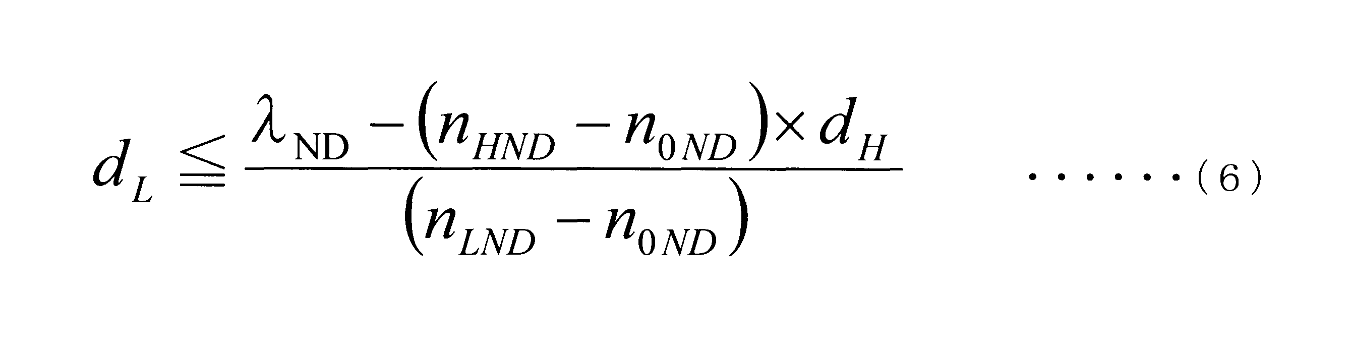
2π・(n1-1)・d1/λ1=2π ・・・・・・(1)
η1(0)=1 ・・・・・・(2)
(1)式において、n1はグレーティング素子の屈折率、d1は溝の深さ、λ1はグレーティング素子により回折されるレーザ光の波長とは異なる波長(実質的に回折されないレーザ光の波長)である。また、(2)式において、η1(0)は波長λ1のレーザ光の0次回折光の光利用効率である。
そして、特許文献1に記載のスカラー回折理論による近似計算では、グレーティング素子を波長λ1のレーザ光が透過する場合、溝間を透過する光線と溝を透過する光線との間の位相差が2πであれば((1)式を満たせば)、溝の深さがどのような深さであっても、(2)式を満たす。即ち、波長λ1のレーザ光の回折効率η1(0)は、Duty比によらず、1となる。つまり、0次回折光の光利用効率は、Duty比によらず100%となるため、溝部の深さは光利用効率と無関係である。
したがって、ベクトル回折理論による厳密計算で求めた0次回折光の光利用効率を向上するためには、格子深さを浅くする(凸部の高さを低くする)とともに、回折させないレーザ光に波長の整数倍の位相差を発生させる深さとすればよい。
(5)式及び(6)式は、誘電体多層膜により形成された凸部の高さをなるべく低くするとともに、回折させないレーザ光に波長の整数倍の位相差を発生させる高さとするための条件である。したがって、(5)式及び(6)式を満たすように、高屈折率材料から形成される誘電膜の膜厚の総和dH、低屈折率材料から形成される誘電膜の膜厚の総和dLを決定することにより、当該厳密計算によって算出した0次回折光の光利用効率を向上させることができる。即ち、(5)式及び(6)式を満たすように、凸部の高さを決定することにより、当該厳密計算によって算出した0次回折光の光利用効率を向上させることができる。
また、グレーティング素子120及びグレーティング素子121では、グレーティング素子12と同様に、誘電体多層膜の層数が、当該誘電体多層膜に入射したレーザ光が当該誘電体多層膜において反射される反射率が低くなるように、決定されている。
さらに、グレーティング素子120及びグレーティング素子121において、格子構造のピッチをP、凸部120G、121Eの幅をWとしたとき、以下の(7)式を満たすことが好ましい。
0.5<W/P<1.0 ・・・・・・(7)
これにより、グレーティング素子120及びグレーティング素子121に入射するレーザ光の反射を効果的に抑制することができる。具体的には、誘電体多層膜に入射したレーザ光が当該誘電体多層膜において反射される反射率が4%以下となるようなDuty(W/P)を選択することが好ましい。
実施例1として、図2に示すグレーティング素子12の実施例を示す。グレーティング素子12を透過するレーザ光は3種類である。3種類のレーザ光の波長は、それぞれ、0.405μm、0.660μm、0.785μmである。
また、回折部材12Aの凸部12G及び回折部材12Bの凸部12Iは誘電体多層膜で形成した。また、回折部材12C及び回折部材12Cの凸部12Kは、同一素材で一体的に形成した。回折部材12C及び凸部12Kは、石英で形成した。
回折部材12Bの回折波長は、0.785μm、非回折波長は、0.405μm、0.660μmである。また、回折部材12Bの格子構造のピッチ(P)は60μm、Duty(W/P)は0.583である。また、凸部12Iの高さ(格子深さ:d)は1.300μmである。回折部材12Bの透明基板12Eの屈折率は、波長0.405μmにおいて1.530、波長0.660μmにおいて1.514、波長0.785μmにおいて1.511である。凸部12Iに隣接する空間の媒質は接着材料であり、当該接着材料の屈折率は、波長0.405μmにおいて1.400、波長0.660μmにおいて1.385、波長0.785μmにおいて1.382である。
回折部材12Cの回折波長は、0.660μm、非回折波長は、0.405μm、0.785μmである。また、回折部材12Cの格子構造のピッチ(P)は50μm、Duty(W/P)は0.500である。また、凸部12Kの高さ(格子深さ:d)は1.645μmである。回折部材12Cの透明基板12Fの屈折率は、波長0.405μmにおいて1.492、波長0.660μmにおいて1.477、波長0.785μmにおいて1.475である。また、凸部12Kの屈折率は、波長0.405μmにおいて1.492、波長0.660μmにおいて1.477、波長0.785μmにおいて1.475である。また、凸部12Kに隣接する空間の媒質は空気であるため、凸部12Kに隣接する空間の媒質の屈折率は1.000である。
回折部材12Aにより波長0.405μm、0.660μm、0.785μmのレーザ光に付加される位相シフト量φ405、φ660、φ785とすると、(8)式より、φ405={(2.223-1.000)×3.483+(1.492-1.000)×0.189}/0.405-Round[{(2.223-1.000)×3.483+(1.492-1.000)×0.189}/0.405]=-0.2498(λ)、φ660={(2.108-1.000)×3.483+(1.477-1.000)×0.189}/0.660-Round[{(2.108-1.000)×3.483+(1.477-1.000)×0.189}/0.660]=-0.0170(λ)、φ785={(2.093-1.000)×3.483+(1.475-1.000)×0.189}/0.785-Round[{(2.093-1.000)×3.483+(1.475-1.000)×0.189}/0.785]=-0.0367(λ)となる。即ち、回折部材12Aにより波長0.405μmのレーザ光に付加される位相シフト量φ405は-0.2498(λ)であり、(3)式を満たしている。また、回折部材12Aにより波長0.660μmのレーザ光及び波長0.785μmのレーザ光に付加される位相シフト量φ660、φ785は-0.0170(λ)、-0.0367(λ)であり、(4)式を満たしている。
また、回折光の強度は、有限差分時間領域法(FDTD法)による厳密計算で求めた。図14では、入射光の強度を100%としたときの各回折次数の回折光の強度を示している。
図15A、図15B、図15Cに示すように、波長0.405μm、0.660μm、0.785μmにおける反射率は2%以下となっている。したがって、回折部材12Aの誘電体多層膜は、反射防止性能を兼ね備えている。また、回折部材12AのDutyは0.700であり、回折部材12Aの表面における凸部12Gの占める割合を多くすることができる。これにより、回折部材12Aに入射するレーザ光の反射を効果的に抑制することができる。そのため、回折部材12Aに反射防止膜を施す必要がない。なお、反射防止膜を別途回折部材12Aの表面に成膜して、さらに反射防止性能を高めても良い。
回折部材12Bにより波長0.405μm、0.660μm、0.785μmのレーザ光に付加される位相シフト量φ405、φ660、φ785とすると、(8)式より、φ405={(2.223-1.400)×0.900+(1.492-1.400)×0.400}/0.405-Round[{(2.223-1.400)×0.900+(1.492-1.400)×0.400}/0.405]=-0.079(λ)、φ660={(2.108-1.385)×0.900+(1.477-1.385)×0.400}/0.660-Round[{(2.108-1.385)×0.900+(1.477-1.385)×0.400}/0.660]=+0.042(λ)、φ785={(2.093-1.382)×0.900+(1.475-1.382)×0.400}/0.785-Round[{(2.093-1.382)×0.900+(1.475-1.382)×0.400}/0.785]=-0.137(λ)となる。即ち、回折部材12Bにより波長0.785μmのレーザ光に付加される位相シフト量φ785は-0.137(λ)であり、(3)式を満たしている。また、回折部材12Bにより波長0.405μmのレーザ光及び波長0.660μmのレーザ光に付加される位相シフト量φ405、φ660は-0.079(λ)、+0.042(λ)であり、(4)式を満たしている。
また、回折光の強度は、有限差分時間領域法(FDTD法)による厳密計算で求めた。図17では、入射光の強度を100%としたときの各回折次数の回折光の強度を示している。
図18A、図18B、図18Cに示すように、波長0.405μm、0.660μm、0.785μmにおける反射率は1%以下となっている。したがって、回折部材12Bの誘電体多層膜は、反射防止性能を兼ね備えている。また、回折部材12BのDutyは0.583であり、回折部材12Bの表面における凸部12Iの占める割合を多くすることができる。これにより、回折部材12Bに入射するレーザ光の反射を効果的に抑制することができる。そのため、回折部材12Bに反射防止膜を施す必要がない。なお、反射防止膜を別途回折部材12Bの表面に成膜して、さらに反射防止性能を高めても良い。
φ=d×(n-n0)/λ-Round(d×(n-n0)/λ)
・・・・・・(9)
したがって、回折部材12Cにより波長0.405μm、0.660μm、0.785μmのレーザ光に付加される位相シフト量φ405、φ660、φ785とすると、(9)式より、φ405=1.645×(1.492-1.000)/0.405-Round[1.645×(1.492-1.000)/0.405]=-0.002(λ)、φ660=1.645×(1.477-1.000)/0.660-Round[1.645×(1.477-1.000)/0.660]=+0.189(λ)、φ785=1.645×(1.475-1.000)/0.785-Round[1.645×(1.475-1.000)/0.785]=-0.005(λ)となる。即ち、回折部材12Cにより波長0.660μmのレーザ光に付加される位相シフト量φ660は+0.189(λ)であり、(3)式を満たしている。また、回折部材12Cにより波長0.405μmのレーザ光及び波長0.785μmのレーザ光に付加される位相シフト量φ405、φ785は-0.002(λ)、-0.005(λ)であり、(4)式を満たしている。
また、回折光の強度は、有限差分時間領域法(FDTD法)による厳密計算で求めた。図19では、入射光の強度を100%としたときの各回折次数の回折光の強度を示している。
なお、回折部材12Cのように1種類の材質からなる場合、反射防止膜を回折部材12Cの表面に成膜することが好ましい。
そして、図1に示すように、実施例1にかかる回折部材12A、12B、12Cを貼り合わせることにより、波長0.405μm、0.660μm、0.785μmのレーザ光を好適な回折効率でそれぞれ独立に回折させることができるグレーティング素子12を得ることができる。
実施例2として、図11に示すグレーティング素子121の実施例を示す。グレーティング素子121を透過するレーザ光は2種類である。2種類のレーザ光の波長は、それぞれ、0.660μm、0.785μmである。
また、回折部材121Aの凸部121Eは誘電体多層膜で形成した。また、回折部材121Bの凸部121Gはアクリル系樹脂で形成した。
回折部材121Bの回折波長は、0.785μm、非回折波長は、0.660μmである。また、回折部材121Bの格子構造のピッチ(P)は35μm、Duty(W/P)は0.24である。また、凸部121Gの高さ(格子深さ:d)は1.320μmである。回折部材121Bの透明基板121Dの屈折率は、波長0.660μmにおいて1.514、波長0.785μmにおいて1.511である。また、凸部121Gの屈折率は、波長0.660μmにおいて1.500、波長0.785μmにおいて1.497である。また、凸部121Gに隣接する空間の媒質は空気であるため、凸部121Gに隣接する空間の媒質の屈折率は1.000である。
また、回折部材121Aにより波長0.660μm、0.785μmのレーザ光に付加される位相シフト量φ660、φ785とすると、(8)式より、φ660={(2.108-1.000)×0.640+(1.477-1.000)×0.120}/0.660-Round[{(2.108-1.000)×0.640+(1.477-1.000)×0.120}/0.660]=+0.161(λ)、φ785={(2.093-1.000)×0.640+(1.475-1.000)×0.120}/0.785-Round[{(2.093-1.000)×0.640+(1.475-1.000)×0.120}/0.785]=-0.036(λ)となる。即ち、回折部材121Aにより波長0.660μmのレーザ光に付加される位相シフト量φ660は+0.161(λ)であり、(3)式を満たしている。また、回折部材121Aにより波長0.785μmのレーザ光に付加される位相シフト量φ785は-0.036(λ)であり、(4)式を満たしている。
また、回折光の強度は、有限差分時間領域法(FDTD法)による厳密計算で求めた。図21では、入射光の強度を100%としたときの各回折次数の回折光の強度を示している。
また、回折光の強度は、有限差分時間領域法(FDTD法)による厳密計算で求めた。図22では、入射光の強度を100%としたときの各回折次数の回折光の強度を示している。
図23に示すように、波長0.660μm、0.785μmにおける反射率は1%以下となっている。したがって、回折部材121Aの誘電体多層膜は、反射防止性能を兼ね備えている。また、回折部材121AのDutyは0.800であり、回折部材121Aの表面における凸部121Eの占める割合を多くすることができる。これにより、回折部材121Aに入射するレーザ光の反射を効果的に抑制することができる。そのため、回折部材121Aに反射防止膜を施す必要がない。なお、反射防止膜を別途回折部材121Aの表面に成膜して、さらに反射防止性能を高めても良い。
また、回折光の強度は、有限差分時間領域法(FDTD法)による厳密計算で求めた。図24では、入射光の強度を100%としたときの各回折次数の回折光の強度を示している。
そして、図11に示すように、実施例2にかかる回折部材121A、121Bを貼り合わせることにより、波長0.660μm、0.785μmのレーザ光を好適な回折効率でそれぞれ独立に回折させることができるグレーティング素子121を得ることができる。
これにより、当該グレーティング素子120、121は、波長の異なる2つのレーザ光を好適に回折することができる。
0.10<|φD|≦0.25 ・・・・・・(3)
0.00≦|φND|≦0.10 ・・・・・・(4)
(3)式及び(4)式を満たすことにより、所定の回折効率で回折させるレーザ光の分光比(1次回折光の強度/0次回折光の強度)を0.05~0.1程度とすることができる。当該分光比の値が0.05より小さくなると、サブスポットの強度が小さくなるため、良好なトラッキング信号を得ることができない。また、当該分光比の値が0.1より大きくなると、メインスポットの強度が小さくなってしまうため、再生信号レベルの低下を招いてしまう。
具体的には、グレーティング素子によりレーザ光に付加する位相シフト量φが大きくなると、0次回折光の強度が低下してしまい、分光比がDuty(回折部材の格子構造のピッチに対する凸部の幅の比率)の変化にしたがって大きく変化してしまう。そのため、所望の分光比を得ようとすると、0次回折光の強度が低下してしまい、再生信号レベルの低下を招いてしまう。一方、当該位相シフト量φが小さくなると、0次回折光の強度は大きくなるが、分光比がDutyを変化させても変化しにくくなり、いずれのDutyにおいても所望の分光比を得るのが難しくなる。
そのため、(3)式及び(4)式を満たすことにより、良好なトラッキング信号を得るとともに再生信号レベルの低下を防ぐことができる。


(5)式及び(6)式を満たすように、凸部120E、121Eの高さを決定することにより、厳密計算によって算出した0次回折光の光利用効率を向上させることができる。
このように構成することにより、誘電体多層膜に入射するレーザ光の反射を抑制することができる。これにより、光源への戻り光を低減できる。そのため、戻り光がレーザ共振器内で干渉し、レーザ出力に変動を引き起こすことを防止することができる。したがって、レーザ雑音を抑制することができる。
また、レーザ光の反射を抑制することができるので、レーザ光を高効率で透過することができる。換言すれば、光利用効率を向上させることができる。
これにより、十分にレーザ雑音を抑制することができる。また、光利用効率を向上させることができる。
0.5<W/P<1.0 ・・・・・・(7)
これにより、反射防止機能を有する凸部12G、12I、120E、121Eの幅を、反射防止機能を有しない凹部12H、12J、120F、121Fの幅より大きくすることができる。そのため、グレーティング素子12、120、121の表面における凸部12G、12I、120E、121Eの占める割合を多くすることができる。これにより、グレーティング素子12、120、121に入射するレーザ光の反射を効果的に抑制することができる。
これにより、グレーティング素子12、120、121内における回折部材12A、12B、12C、120A、120B、121A、121Bの位置ずれを防止できる。さらに、接着材料として所望の屈折率を有する接着材料を用いることにより、グレーティング素子12、120、121の回折効率及び0次回折光利用効率を好適な値にすることができる。
11 レーザユニット(光源)
111 CD用レーザ光源
112 DVD用レーザ光源
113 BD用レーザ光源
12、120、121 グレーティング素子(光学素子)
12A、12B、12C、120A、120B、121A、121B 回折部材
12D、12E、12F、120C、120D、121C、121D 透明基板
12G、12I、12K、120E、120G、121E、121G 凸部
12H、12J、12L、120F、120H、121F、121H 凹部
17 CD
18 DVD
19 BD
Claims (21)
- 透明基板の一方の表面に凸部と凹部とが周期的に配置されてなる回折部材を複数備え、
複数の前記回折部材は、前記透明基板に略垂直な方向に積層されており、
複数の前記回折部材のうち、少なくとも1つの前記回折部材の前記凸部は、誘電体多層膜により形成され、
前記誘電体多層膜は、前記透明基板上に2種類以上の誘電膜が前記略垂直な方向に積層されてなり、
複数の前記回折部材が所定の回折効率で回折させるレーザ光の波長はそれぞれ異なるグレーティング素子。 - 3つの前記回折部材が前記略垂直な方向に積層されてなる請求項1に記載のグレーティング素子。
- 2つの前記回折部材が前記略垂直な方向に積層されてなる請求項1に記載のグレーティング素子。
- 前記凸部が前記誘電体多層膜により形成されている前記回折部材において、前記所定の回折効率で回折させるレーザ光に付加する位相シフト量をφD、実質的に回折させないレーザ光に付加する位相シフト量をφNDとしたとき、以下の(3)式及び(4)式を満たす請求項1又は2に記載のグレーティング素子。
0.10<|φD|≦0.25 ・・・・・・(3)
0.00≦|φND|≦0.10 ・・・・・・(4) - 前記凸部が前記誘電体多層膜により形成されている前記回折部材において、前記所定の回折効率で回折させるレーザ光に付加する位相シフト量をφD、実質的に回折させないレーザ光に付加する位相シフト量をφNDとしたとき、以下の(3)式及び(4)式を満たす請求項3に記載のグレーティング素子。
0.10<|φD|≦0.25 ・・・・・・(3)
0.00≦|φND|≦0.10 ・・・・・・(4) - 前記誘電体多層膜は、高屈折率材料から形成される前記誘電膜と、低屈折率材料から形成される前記誘電膜と、が積層されてなり、
前記凸部が前記誘電体多層膜により形成されている前記回折部材において、前記所定の回折効率で回折させるレーザ光の波長をλD、実質的に回折させないレーザ光の波長をλND、前記高屈折率材料の波長λNDにおける屈折率をnHND、前記低屈折率材料の波長λNDにおける屈折率をnLND、前記誘電体多層膜に隣接する空間の媒質の屈折率をn0ND、前記高屈折率材料から形成される前記誘電膜の膜厚の総和をdH、前記低屈折率材料から形成される前記誘電膜の膜厚の総和をdLとしたとき、以下の(5)式及び(6)式を満たす請求項3又は5に記載のグレーティング素子。
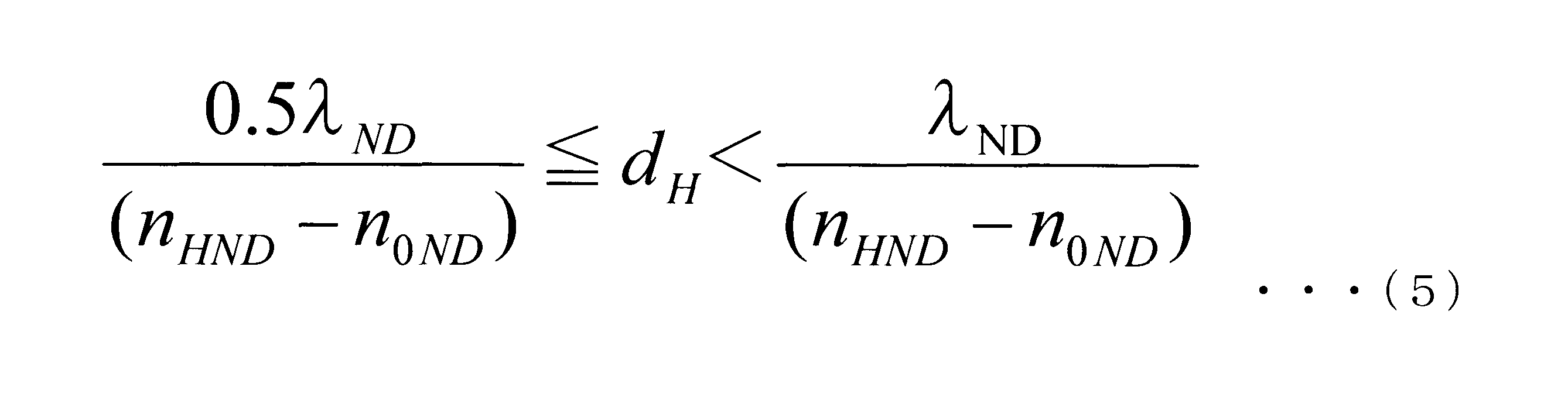
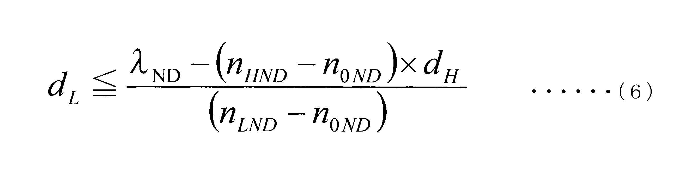
- 前記誘電体多層膜は、高屈折率材料から形成される前記誘電膜と、低屈折率材料から形成される前記誘電膜と、が交互に積層されてなる請求項1乃至6の何れか一項に記載のグレーティング素子。
- 前記誘電体多層膜に入射したレーザ光が当該誘電体多層膜により反射される割合である反射率が4%以下である請求項1乃至7の何れか一項に記載のグレーティング素子。
- 前記凸部が前記誘電体多層膜により形成されている前記回折部材において、当該回折部材の格子構造のピッチをP、前記凸部の幅をWとしたとき、以下の(7)式を満たす請求項1乃至8の何れか一項に記載のグレーティング素子。
0.5<W/P<1.0 ・・・・・・(7) - 複数の前記回折部材は、互いに接着材料により接着されている請求項1乃至9の何れか一項に記載のグレーティング素子。
- 波長の異なる複数のレーザ光を出射する複数のレーザ光源を備えるレーザユニットを光源として備え、
前記レーザユニットから出射されたレーザ光の光路上に、請求項1乃至10の何れか一項に記載のグレーティング素子が配置されている光ピックアップ光学系。 - 透明基板の一方の表面に凸部と凹部とが周期的に配置されてなる回折部材を複数備えるグレーティング素子の設計方法であって、
複数の前記回折部材を、前記透明基板に略垂直な方向に積層し、
複数の前記回折部材のうち、少なくとも1つの前記回折部材の前記凸部を、誘電体多層膜により形成し、
前記誘電体多層膜を、前記透明基板上に2種類以上の誘電膜を前記略垂直な方向に積層することにより形成し、
複数の前記回折部材が所定の回折効率で回折させるレーザ光の波長はそれぞれ異なるグレーティング素子の設計方法。 - 3つの前記回折部材を前記略垂直な方向に積層する請求項12に記載のグレーティング素子の設計方法。
- 2つの前記回折部材を前記略垂直な方向に積層する請求項12に記載のグレーティング素子の設計方法。
- 前記凸部が前記誘電体多層膜により形成されている前記回折部材において、前記所定の回折効率で回折させるレーザ光に付加する位相シフト量をφD、実質的に回折させないレーザ光に付加する位相シフト量をφNDとしたとき、以下の(3)式及び(4)式を満たす請求項12又は13に記載のグレーティング素子の設計方法。
0.10<|φD|≦0.25 ・・・・・・(3)
0.00≦|φND|≦0.10 ・・・・・・(4) - 前記凸部が前記誘電体多層膜により形成されている前記回折部材において、前記所定の回折効率で回折させるレーザ光に付加する位相シフト量をφD、実質的に回折させないレーザ光に付加する位相シフト量をφNDとしたとき、以下の(3)式及び(4)式を満たす請求項14に記載のグレーティング素子の設計方法。
0.10<|φD|≦0.25 ・・・・・・(3)
0.00≦|φND|≦0.10 ・・・・・・(4) - 前記誘電体多層膜を、高屈折率材料から形成される前記誘電膜と、低屈折率材料から形成される前記誘電膜と、を積層することにより形成し、
前記凸部が前記誘電体多層膜により形成されている前記回折部材において、前記所定の回折効率で回折させるレーザ光の波長をλD、実質的に回折させないレーザ光の波長をλND、前記高屈折率材料の波長λNDにおける屈折率をnHND、前記低屈折率材料の波長λNDにおける屈折率をnLND、前記誘電体多層膜に隣接する空間の媒質の屈折率をn0ND、前記高屈折率材料から形成される前記誘電膜の膜厚の総和をdH、前記低屈折率材料から形成される前記誘電膜の膜厚の総和をdLとしたとき、以下の(5)式及び(6)式を満たす請求項14又は16に記載のグレーティング素子の設計方法。

- 前記誘電体多層膜を、高屈折率材料から形成される前記誘電膜と、低屈折率材料から形成される前記誘電膜と、を交互に積層することにより形成する請求項12乃至17の何れか一項に記載のグレーティング素子の設計方法。
- 前記誘電体多層膜に入射したレーザ光が当該誘電体多層膜により反射される割合である反射率が4%以下である請求項12乃至18の何れか一項に記載のグレーティング素子の設計方法。
- 前記凸部が前記誘電体多層膜により形成されている前記回折部材において、当該回折部材の格子構造のピッチをP、前記凸部の幅をWとしたとき、以下の(7)式を満たす請求項12乃至19の何れか一項に記載のグレーティング素子の設計方法。
0.5<W/P<1.0 ・・・・・・(7) - 複数の前記回折部材を、互いに接着材料により接着する請求項12乃至20の何れか一項に記載のグレーティング素子の設計方法。
Priority Applications (3)
| Application Number | Priority Date | Filing Date | Title |
|---|---|---|---|
| US12/995,761 US20110085432A1 (en) | 2008-11-05 | 2009-10-29 | Grating element, optical pickup optical system and method of designing grating element |
| JP2010536663A JPWO2010052863A1 (ja) | 2008-11-05 | 2009-10-29 | グレーティング素子、光ピックアップ光学系及びグレーティング素子の設計方法 |
| CN200980131102.4A CN102119415A (zh) | 2008-11-05 | 2009-10-29 | 光栅元件、光拾取光学系统以及光栅元件的设计方法 |
Applications Claiming Priority (2)
| Application Number | Priority Date | Filing Date | Title |
|---|---|---|---|
| JP2008-283995 | 2008-11-05 | ||
| JP2008283995 | 2008-11-05 |
Publications (1)
| Publication Number | Publication Date |
|---|---|
| WO2010052863A1 true WO2010052863A1 (ja) | 2010-05-14 |
Family
ID=42152676
Family Applications (1)
| Application Number | Title | Priority Date | Filing Date |
|---|---|---|---|
| PCT/JP2009/005734 Ceased WO2010052863A1 (ja) | 2008-11-05 | 2009-10-29 | グレーティング素子、光ピックアップ光学系及びグレーティング素子の設計方法 |
Country Status (4)
| Country | Link |
|---|---|
| US (1) | US20110085432A1 (ja) |
| JP (1) | JPWO2010052863A1 (ja) |
| CN (1) | CN102119415A (ja) |
| WO (1) | WO2010052863A1 (ja) |
Cited By (4)
| Publication number | Priority date | Publication date | Assignee | Title |
|---|---|---|---|---|
| JP2013228688A (ja) * | 2012-03-26 | 2013-11-07 | Asahi Glass Co Ltd | 透過型回折素子 |
| JP2021099399A (ja) * | 2019-12-20 | 2021-07-01 | 浜松ホトニクス株式会社 | テラヘルツ波用レンズ及びテラヘルツ波用レンズの製造方法 |
| JP2021099400A (ja) * | 2019-12-20 | 2021-07-01 | 浜松ホトニクス株式会社 | テラヘルツ波用光学素子及びテラヘルツ波用光学素子の製造方法 |
| JP2023029913A (ja) * | 2017-06-30 | 2023-03-07 | 大日本印刷株式会社 | 回折光学素子形成用のアクリル系樹脂組成物 |
Families Citing this family (1)
| Publication number | Priority date | Publication date | Assignee | Title |
|---|---|---|---|---|
| WO2020082216A1 (zh) * | 2018-10-22 | 2020-04-30 | 歌尔股份有限公司 | 衍射波导装置、显示装置及制造方法 |
Citations (3)
| Publication number | Priority date | Publication date | Assignee | Title |
|---|---|---|---|---|
| JP2006073042A (ja) * | 2004-08-31 | 2006-03-16 | Asahi Glass Co Ltd | 回折素子および光ヘッド装置 |
| JP2008216882A (ja) * | 2007-03-07 | 2008-09-18 | Nitto Koki Kk | 透過型回折素子、光ピックアップ装置及び透過型回折素子の製造方法 |
| JP2008217954A (ja) * | 2007-03-08 | 2008-09-18 | Epson Toyocom Corp | 回折格子およびそれを用いた光学ヘッド装置 |
Family Cites Families (5)
| Publication number | Priority date | Publication date | Assignee | Title |
|---|---|---|---|---|
| JP3062099B2 (ja) * | 1996-02-06 | 2000-07-10 | 日本電気株式会社 | 光ヘッド装置 |
| JP4359713B2 (ja) * | 2000-11-24 | 2009-11-04 | コニカミノルタホールディングス株式会社 | 回折光学素子 |
| JP2003067972A (ja) * | 2001-05-29 | 2003-03-07 | Nec Corp | 光ヘッド装置および光学式情報記録再生装置 |
| JP4396413B2 (ja) * | 2004-06-22 | 2010-01-13 | ソニー株式会社 | 光ピックアップ装置、光ディスク装置 |
| US8064314B2 (en) * | 2005-07-28 | 2011-11-22 | Panasonic Corporation | Optical head and optical disc device |
-
2009
- 2009-10-29 CN CN200980131102.4A patent/CN102119415A/zh active Pending
- 2009-10-29 US US12/995,761 patent/US20110085432A1/en not_active Abandoned
- 2009-10-29 JP JP2010536663A patent/JPWO2010052863A1/ja active Pending
- 2009-10-29 WO PCT/JP2009/005734 patent/WO2010052863A1/ja not_active Ceased
Patent Citations (3)
| Publication number | Priority date | Publication date | Assignee | Title |
|---|---|---|---|---|
| JP2006073042A (ja) * | 2004-08-31 | 2006-03-16 | Asahi Glass Co Ltd | 回折素子および光ヘッド装置 |
| JP2008216882A (ja) * | 2007-03-07 | 2008-09-18 | Nitto Koki Kk | 透過型回折素子、光ピックアップ装置及び透過型回折素子の製造方法 |
| JP2008217954A (ja) * | 2007-03-08 | 2008-09-18 | Epson Toyocom Corp | 回折格子およびそれを用いた光学ヘッド装置 |
Cited By (9)
| Publication number | Priority date | Publication date | Assignee | Title |
|---|---|---|---|---|
| JP2013228688A (ja) * | 2012-03-26 | 2013-11-07 | Asahi Glass Co Ltd | 透過型回折素子 |
| JP2023029913A (ja) * | 2017-06-30 | 2023-03-07 | 大日本印刷株式会社 | 回折光学素子形成用のアクリル系樹脂組成物 |
| JP7542592B2 (ja) | 2017-06-30 | 2024-08-30 | 大日本印刷株式会社 | 回折光学素子形成用のアクリル系樹脂組成物 |
| JP2021099399A (ja) * | 2019-12-20 | 2021-07-01 | 浜松ホトニクス株式会社 | テラヘルツ波用レンズ及びテラヘルツ波用レンズの製造方法 |
| JP2021099400A (ja) * | 2019-12-20 | 2021-07-01 | 浜松ホトニクス株式会社 | テラヘルツ波用光学素子及びテラヘルツ波用光学素子の製造方法 |
| JP7455569B2 (ja) | 2019-12-20 | 2024-03-26 | 浜松ホトニクス株式会社 | テラヘルツ波用レンズ及びテラヘルツ波用レンズの製造方法 |
| JP7455570B2 (ja) | 2019-12-20 | 2024-03-26 | 浜松ホトニクス株式会社 | テラヘルツ波用光学素子及びテラヘルツ波用光学素子の製造方法 |
| US12032184B2 (en) | 2019-12-20 | 2024-07-09 | Hamamatsu Photonics K.K. | Terahertz wave lens and method for producing terahertz wave lens |
| US12135444B2 (en) | 2019-12-20 | 2024-11-05 | Hamamatsu Photonics K.K. | Terahertz wave optical element and method for producing terahertz wave optical element |
Also Published As
| Publication number | Publication date |
|---|---|
| CN102119415A (zh) | 2011-07-06 |
| JPWO2010052863A1 (ja) | 2012-04-05 |
| US20110085432A1 (en) | 2011-04-14 |
Similar Documents
| Publication | Publication Date | Title |
|---|---|---|
| US8279737B2 (en) | Diffraction grating, aberration correction element and optical head device | |
| JP2004508655A (ja) | 光走査デバイス | |
| JP2011187139A (ja) | グレーティング素子及びその製造方法、並びに、そのグレーティング素子を用いた光ピックアップ装置 | |
| JPWO2010052863A1 (ja) | グレーティング素子、光ピックアップ光学系及びグレーティング素子の設計方法 | |
| JP5146317B2 (ja) | 回折素子およびこれを備えた光ヘッド装置 | |
| JP2006073042A (ja) | 回折素子および光ヘッド装置 | |
| JP4218240B2 (ja) | 光ヘッド装置 | |
| JPWO2007069660A1 (ja) | 波長選択回折素子及び光ヘッド装置 | |
| JP4742630B2 (ja) | 反射光学素子および光ピックアップ装置 | |
| JP2007234094A (ja) | 回折格子体、これを用いた光ヘッド装置及び回折格子体の製造方法 | |
| JP2008217954A (ja) | 回折格子およびそれを用いた光学ヘッド装置 | |
| JP2010020855A (ja) | 複数波長用反射型回折格子およびこれを備えた光ピックアップ装置 | |
| JP5234151B2 (ja) | 回折素子および光ヘッド装置 | |
| JP4645938B2 (ja) | 光学部品及び光ピックアップ装置 | |
| JP5082792B2 (ja) | 光ヘッド装置 | |
| JP2011008186A (ja) | グレーティング素子及びグレーティング素子の設計方法 | |
| JP5382124B2 (ja) | 光ピックアップ装置 | |
| JP2000339741A (ja) | 光学ピックアップ装置 | |
| CN101288124B (zh) | 衍射光学元件及光学头装置 | |
| JP4404189B2 (ja) | 回折素子および光ヘッド装置 | |
| JP2013077374A (ja) | 回折素子および光ヘッド装置 | |
| JP2002170272A (ja) | 光ヘッド装置 | |
| JP2007317326A (ja) | 回折格子とその製造方法、及び光ピックアップ装置 | |
| JP2013093070A (ja) | 回折光学素子及び光ヘッド装置 | |
| JP2011054273A (ja) | 偏光性回折素子 |
Legal Events
| Date | Code | Title | Description |
|---|---|---|---|
| WWE | Wipo information: entry into national phase |
Ref document number: 200980131102.4 Country of ref document: CN |
|
| 121 | Ep: the epo has been informed by wipo that ep was designated in this application |
Ref document number: 09824564 Country of ref document: EP Kind code of ref document: A1 |
|
| WWE | Wipo information: entry into national phase |
Ref document number: 2010536663 Country of ref document: JP |
|
| WWE | Wipo information: entry into national phase |
Ref document number: 12995761 Country of ref document: US |
|
| NENP | Non-entry into the national phase |
Ref country code: DE |
|
| 122 | Ep: pct application non-entry in european phase |
Ref document number: 09824564 Country of ref document: EP Kind code of ref document: A1 |