WO2010046392A2 - Electrochemical coating method - Google Patents
Electrochemical coating method Download PDFInfo
- Publication number
- WO2010046392A2 WO2010046392A2 PCT/EP2009/063793 EP2009063793W WO2010046392A2 WO 2010046392 A2 WO2010046392 A2 WO 2010046392A2 EP 2009063793 W EP2009063793 W EP 2009063793W WO 2010046392 A2 WO2010046392 A2 WO 2010046392A2
- Authority
- WO
- WIPO (PCT)
- Prior art keywords
- deposition
- layer
- pulse
- coating method
- pulses
- Prior art date
Links
Classifications
-
- C—CHEMISTRY; METALLURGY
- C25—ELECTROLYTIC OR ELECTROPHORETIC PROCESSES; APPARATUS THEREFOR
- C25D—PROCESSES FOR THE ELECTROLYTIC OR ELECTROPHORETIC PRODUCTION OF COATINGS; ELECTROFORMING; APPARATUS THEREFOR
- C25D5/00—Electroplating characterised by the process; Pretreatment or after-treatment of workpieces
- C25D5/60—Electroplating characterised by the structure or texture of the layers
- C25D5/615—Microstructure of the layers, e.g. mixed structure
- C25D5/617—Crystalline layers
-
- C—CHEMISTRY; METALLURGY
- C23—COATING METALLIC MATERIAL; COATING MATERIAL WITH METALLIC MATERIAL; CHEMICAL SURFACE TREATMENT; DIFFUSION TREATMENT OF METALLIC MATERIAL; COATING BY VACUUM EVAPORATION, BY SPUTTERING, BY ION IMPLANTATION OR BY CHEMICAL VAPOUR DEPOSITION, IN GENERAL; INHIBITING CORROSION OF METALLIC MATERIAL OR INCRUSTATION IN GENERAL
- C23C—COATING METALLIC MATERIAL; COATING MATERIAL WITH METALLIC MATERIAL; SURFACE TREATMENT OF METALLIC MATERIAL BY DIFFUSION INTO THE SURFACE, BY CHEMICAL CONVERSION OR SUBSTITUTION; COATING BY VACUUM EVAPORATION, BY SPUTTERING, BY ION IMPLANTATION OR BY CHEMICAL VAPOUR DEPOSITION, IN GENERAL
- C23C18/00—Chemical coating by decomposition of either liquid compounds or solutions of the coating forming compounds, without leaving reaction products of surface material in the coating; Contact plating
- C23C18/16—Chemical coating by decomposition of either liquid compounds or solutions of the coating forming compounds, without leaving reaction products of surface material in the coating; Contact plating by reduction or substitution, e.g. electroless plating
- C23C18/1601—Process or apparatus
- C23C18/1633—Process of electroless plating
- C23C18/1646—Characteristics of the product obtained
- C23C18/165—Multilayered product
- C23C18/1653—Two or more layers with at least one layer obtained by electroless plating and one layer obtained by electroplating
-
- C—CHEMISTRY; METALLURGY
- C23—COATING METALLIC MATERIAL; COATING MATERIAL WITH METALLIC MATERIAL; CHEMICAL SURFACE TREATMENT; DIFFUSION TREATMENT OF METALLIC MATERIAL; COATING BY VACUUM EVAPORATION, BY SPUTTERING, BY ION IMPLANTATION OR BY CHEMICAL VAPOUR DEPOSITION, IN GENERAL; INHIBITING CORROSION OF METALLIC MATERIAL OR INCRUSTATION IN GENERAL
- C23C—COATING METALLIC MATERIAL; COATING MATERIAL WITH METALLIC MATERIAL; SURFACE TREATMENT OF METALLIC MATERIAL BY DIFFUSION INTO THE SURFACE, BY CHEMICAL CONVERSION OR SUBSTITUTION; COATING BY VACUUM EVAPORATION, BY SPUTTERING, BY ION IMPLANTATION OR BY CHEMICAL VAPOUR DEPOSITION, IN GENERAL
- C23C18/00—Chemical coating by decomposition of either liquid compounds or solutions of the coating forming compounds, without leaving reaction products of surface material in the coating; Contact plating
- C23C18/16—Chemical coating by decomposition of either liquid compounds or solutions of the coating forming compounds, without leaving reaction products of surface material in the coating; Contact plating by reduction or substitution, e.g. electroless plating
- C23C18/31—Coating with metals
-
- C—CHEMISTRY; METALLURGY
- C25—ELECTROLYTIC OR ELECTROPHORETIC PROCESSES; APPARATUS THEREFOR
- C25D—PROCESSES FOR THE ELECTROLYTIC OR ELECTROPHORETIC PRODUCTION OF COATINGS; ELECTROFORMING; APPARATUS THEREFOR
- C25D15/00—Electrolytic or electrophoretic production of coatings containing embedded materials, e.g. particles, whiskers, wires
-
- C—CHEMISTRY; METALLURGY
- C25—ELECTROLYTIC OR ELECTROPHORETIC PROCESSES; APPARATUS THEREFOR
- C25D—PROCESSES FOR THE ELECTROLYTIC OR ELECTROPHORETIC PRODUCTION OF COATINGS; ELECTROFORMING; APPARATUS THEREFOR
- C25D5/00—Electroplating characterised by the process; Pretreatment or after-treatment of workpieces
- C25D5/10—Electroplating with more than one layer of the same or of different metals
-
- C—CHEMISTRY; METALLURGY
- C25—ELECTROLYTIC OR ELECTROPHORETIC PROCESSES; APPARATUS THEREFOR
- C25D—PROCESSES FOR THE ELECTROLYTIC OR ELECTROPHORETIC PRODUCTION OF COATINGS; ELECTROFORMING; APPARATUS THEREFOR
- C25D5/00—Electroplating characterised by the process; Pretreatment or after-treatment of workpieces
- C25D5/18—Electroplating using modulated, pulsed or reversing current
-
- C—CHEMISTRY; METALLURGY
- C25—ELECTROLYTIC OR ELECTROPHORETIC PROCESSES; APPARATUS THEREFOR
- C25D—PROCESSES FOR THE ELECTROLYTIC OR ELECTROPHORETIC PRODUCTION OF COATINGS; ELECTROFORMING; APPARATUS THEREFOR
- C25D5/00—Electroplating characterised by the process; Pretreatment or after-treatment of workpieces
- C25D5/48—After-treatment of electroplated surfaces
-
- C—CHEMISTRY; METALLURGY
- C25—ELECTROLYTIC OR ELECTROPHORETIC PROCESSES; APPARATUS THEREFOR
- C25D—PROCESSES FOR THE ELECTROLYTIC OR ELECTROPHORETIC PRODUCTION OF COATINGS; ELECTROFORMING; APPARATUS THEREFOR
- C25D5/00—Electroplating characterised by the process; Pretreatment or after-treatment of workpieces
- C25D5/627—Electroplating characterised by the visual appearance of the layers, e.g. colour, brightness or mat appearance
-
- C—CHEMISTRY; METALLURGY
- C25—ELECTROLYTIC OR ELECTROPHORETIC PROCESSES; APPARATUS THEREFOR
- C25D—PROCESSES FOR THE ELECTROLYTIC OR ELECTROPHORETIC PRODUCTION OF COATINGS; ELECTROFORMING; APPARATUS THEREFOR
- C25D3/00—Electroplating: Baths therefor
- C25D3/66—Electroplating: Baths therefor from melts
- C25D3/665—Electroplating: Baths therefor from melts from ionic liquids
Definitions
- the invention relates to an electrochemical coating method for the deposition of at least one layer on at least one workpiece in a deposition bath, comprising at least one deposition sequence that is repeated at least once, wherein at least two individual sequences are provided within the at least one deposition sequence, and each individual sequence is a specific deposition method and its use.
- a method of the type mentioned in the opening paragraph is disclosed in CA 2 365 749 A. It relates to a method for producing in particular a gold-tin alloy, in which in a first step, a first component of the alloy and in a second step, the second component of the alloy is deposited.
- the deposition method used in both steps is a classical pulse separation (Unipolar Pulse Plating).
- the different constituents of the alloy are preferably deposited according to the selected current density, always using the same deposition method.
- DE 40 09 914 A1 discloses a method in which a three-layer system is applied to a workpiece, wherein a second layer in the form of a zinc-nickel alloy is connected to a first layer of cobalt. Both layers are deposited by means of DC methods. This is followed by an electrolessly deposited chromate layer.
- EP 1 122 989 B1 describes the combination of direct current with a reverse pulse method for depositing two layers. A similar method for depositing several layers can also be found in JP 2000-173 949 A.
- Pulsed Pulse Plating multipulse system with cathodic and anodic phase, a sequence consists of up to 500 single pulses (Fig. 4)
- Simple pulse sequences each consist of one type of cathodic and anodic pulses (reverse pulse plating). Such a method can be found for example in US 2002/033341 A.
- a base current In addition to the variation and combination of different individual pulses within a sequence, a base current, a direct current, to which the actual pulse sequence is applied, is frequently also used.
- pulse deposition By pulse deposition, several material properties of the deposited metal can be selectively changed. Behind this is always a variation of the electrochemical conditions on the setting of the individual pulse parameters during the deposition. While in DC deposition, the process can be varied only by the amount of current used for deposition (via the average current density), the user has a considerable set of different parameters available in pulse or inverse pulse separation. In addition to the average current density, these are the cathodic and anodic pulse current density, the cathodic and anodic pulse duration, the length of the pulse pause and the pulse frequency.
- Derived quantities such as the duty cycle (ratio of the sum of the pulse durations per sequence to the sum of the length of the pulse pauses per sequence) and the ratio of anodic to cathodic current quantity per sequence are further important factors influencing the pulse deposition process. However, many of these parameters can not be varied completely independently of each other because they partially influence each other. The maximum pulse rate affects the structure and properties of the deposited metal layer.
- the aim is to have a very finely crystalline metal precipitate with primary crystal sizes in the nanometer range.
- the maximum pulse frequency (and thus the minimum possible pulse duration) is determined by the charge for charging (and discharging) the elec- trolytic bilayer necessary time determined. If this limit time is undershot, marked distortions of the applied rectangular pulses occur at the electrode surface (the workpiece to be coated), and the pulse deposition becomes uncontrollable and difficult to reproduce. Therefore, the process and the pulse sequence must be defined such that the time in which the charge and discharge of the double layer takes place is shorter than the pulse duration or the break after the pulse. It must be carried out separately for each electrolyte system a determination of the charging and discharging times.
- the limitation by the mass transport is based on the depletion of the cations in the diffusion layer at the electrode or workpiece surface.
- the pulse deposition can directly influence the structure and the thickness of the diffusion layers.
- the metal ion concentration fluctuates in the rhythm of the pulse frequency, this is called a pulsating diffusion layer.
- This is followed by another diffusion layer with a constant concentration gradient (stationary diffusion layer).
- the depletion of cations in the pulsating diffusion layer limits the pulse current density, the depletion in the outer diffusion layer limits the average current density.
- the practical current density can thus be slightly increased in comparison to direct current, a further increase in the mean current densities succeeds only when manipulating the current density distribution in the reverse pulse separation.
- pulse current deposition is an improvement in precipitation properties that depends on the precipitation structure.
- the precipitation structure is determined on the one hand by the formation of the primary crystallites of the deposited metal, and on the other by the further growth of these crystallites.
- the ratio of crystallite formation to crystallite growth can be affected by pulse deposition (e.g., via pulse current density), pulse rate or duty cycle.
- the classic and probably best-described application for pulse separation is printed circuit board production.
- the copper system is considered a model substance.
- each individual layer is deposited using one of the types of methods described above. However, this limits the material properties of the respective deposited layer. Furthermore, previously known only layer systems, which have a maximum of three individual layers.
- the individual sequences change each other and are repeated at certain intervals.
- the number of single pulses used, which are assigned to the individual sequences, goes into the hundreds.
- layer properties can be achieved that can not be achieved with DC deposits, chemical deposits or conventional pulse depositions.
- the coating uniformity increases.
- the following results can be achieved by suitable combination of the individual sequences:
- Tribological and hardness-related graded coating systems Parallel installation of micro- or nanoparticles;
- each single sequence comprises at least one of the following deposition methods:
- electrochemical pulse plating deposition and pulse reverse plating deposition electrochemical multipulse can be used in particular.
- the deposition sequences used in the multipulse deposition according to the invention can consist, for example, of the following building blocks:
- Pulse phase consisting of 2 - 500 either cathodic or anodic single pulses, each with the same or different pulse current density and pulse length, each followed by either
- a cathodic pulse which differs from the preceding pulse in one or more of the pulse parameter pulse current density, pulse length, pulse shape or pulse frequency or
- Pulse current phase consisting of 2 - 500 either cathodic or anodic single pulses each with the same or different pulse current density and pulse length but different current density or pulse length or pulse frequency to phase 1 respectively followed by either
- a cathodic pulse which differs from the preceding pulse in one or more of the pulse parameter pulse current density, pulse length, pulse shape or pulse frequency or
- An anodic pulse of any desired pulse current density, pulse length, pulse shape or pulse frequency (A ')
- Pulse current phase consisting of 2 - 500 either cathodic or anodic single pulses, each with the same or different pulse current density and pulse length, each followed by (B ')
- a cathodic pulse which differs from the preceding pulse in the pulse current density and pulse length, pulse shape or
- a pulse phase consisting of one in the number of individual pulses within 2-500 arbitrary series of pulses each followed by either (B ")
- a pulse phase of equal or opposite polarization consisting of one in the number of individual pulses within 2-500 arbitrary series of pulses each followed by either (C )
- the length of the individual pulses and phases is in each case between 0.1 and 10,000 ms.
- the current densities of the respective pulses or direct currents are between 0.01 A / dm2 and 100 A / dm2.
- the individual phases can be applied with potential or current (density) in a controlled manner.
- a break is advantageously provided between at least two successive individual sequences and / or after the expiration of a deposition sequence. This pause is obtained by the interruption of the externally supplied current.
- the method according to the invention has a periodic sequence which has at least one DC phase followed by a pulse current phase.
- the individual sequences or else the entire deposition sequence is superimposed with a base current, wherein the base current advantageously has between 1% and 75% of the current density.
- the method according to the invention allows in particular a specific adjustment and change of the material properties of the applied layer if the duration of a single sequence is between 1 and 3000 microseconds.
- the deposition takes place here from a deposition bath containing at least one aqueous solution of at least one salt or mixtures of salts, at least one molten salt or at least one ionic liquid or mixtures thereof.
- the deposition bath additionally contains solids for incorporation into the at least one deposited layer.
- solids include, in particular, particles, fibers, flakes and / or nanotubes (microscopically small, in particular tubular, structures with a diameter smaller than 100 nanometers).
- the object is furthermore achieved by the coating method according to the invention in that the coating has at least four layers.
- the layers can be applied by means of at least one of the following methods, wherein preferably at least two layers are applied with respectively different methods:
- the multilayers can be combined in any order. Due to the selected combination, the resulting properties of the entire layer system can be controlled in a targeted manner.
- the coating has four, five, six, seven, eight, nine, ten, eleven or twelve layers.
- a first primary layer applied to the workpiece is followed by at least one second layer, which has a greater layer thickness than the primary layer.
- the primary layer optionally allows better adhesion of the subsequent layer.
- the second layer is followed by at least one third outer layer whose layer thickness is smaller than that of the second.
- the third layer acts as a barrier against environmental influences of a chemical and / or mechanical nature.
- the second layer is produced by means of an electroless process, and the primary layer and / or the final layer is produced by means of the multipulse process according to the invention.
- the coating method according to the invention has proven particularly suitable for the use for depositing at least one layer on a metallic or non-metallic workpiece with a metallic coating, in particular it is suitable for workpieces made of aluminum, magnesium or titanium.
- the application of layer systems with special material properties by the method according to the invention also allows the use of these materials in areas which in particular have high demands on the wear resistance of the workpieces.
- the individual layer layers as components of a total layer system can consist in particular of the following materials: electrolytically deposited metals and their alloys: nickel (in particular also taking into account the nickel-phosphorus ratio), copper, tin, silver, platinum, gold, zinc, rhodium, antimony , Chromium, cadmium, iron, cobalt, indium, tungsten, rhenium, bismuth, manganese; chemically (without external power) deposited layers of the aforementioned metals and their alloys;
- heat treatments and / or cleaning steps can be carried out between the individual layers.
- FIG. 6 graphically depicts a deposition sequence P consisting of three individual sequences, namely a superimposed pulse plating sequence A, a unipolar pulse plating sequence B and a pulsed pulse plating sequence C.
- the individual sequences A, B, C are interrupted by pulse pauses D. whose length is for example 5 ms, whereby in this case the power supply is interrupted from the outside.
- This deposition sequence P is repeated up to 500 times in this embodiment of the coating process according to the invention.
- the layer properties can be significantly influenced by the multipulse method.
- An example of nickel shows that the structure of the layer can be flipped into lamellar (Fig. 8) only by employing the columnar multipole method of the present invention (Fig. 7) made according to the prior art reverse-pulse technique , It is also possible according to the invention to produce mixed types (FIG. 9) between columnar and lamellar.
- electrolyte composition nickel sulfamate type, temperature 45 ° C.
- Pulse parameter (Fiq.7 1 )
- the nickel layers produced in this experiment by means of the multipulse method according to the invention have by far the highest microhardness.
- the general layer structure (columnar / fine-crystalline / lamellar) can also be changed according to the invention.
- the anodic portion plays an essential role in the deposition sequence.
- the applied current is varied by, for example, pulses, the nature of the adsorbed species may change, and depending on the rate constant of the adsorption, the surface diffusion changes. This leads to different crystallization mechanisms and properties of the deposited precipitate.
- All starting materials to be coated can be pretreated or activated in a manner known per se in preparation for a galvanic coating.
- E2a chemical nickel bath with phosphorus content 2 - 4%
- E2b chemical nickel bath with phosphorus content 4 - 9%
- E2c chemical nickel bath with phosphorus content 9 - 12%
- Substrate Aluminum alloy AISi20Fe5Ni2 Layer system:
- Substrate Aluminum alloy AISi20Fe5Ni2 Layer system:
- Substrate Aluminum Alloy Layer:
- Fig. 11 from left to right:
- Substrate Steel Layer:
- Inventive method Shelf life of the layer system in the above-mentioned thermal shock test without occurrence of bubbles, flaking or cracking.
- Substrate Steel Layer:
- Fig. 12 from bottom to top:
- Substrate Aluminum alloy Schichtsvstem:
- Substrate Aluminum alloy coating system:
Abstract
The invention relates to an electrochemical coating method for depositing at least one layer on at least one work piece in a deposition bath, comprising at least one deposition sequence (P) that is repeated at least once, wherein provided within the at least one deposition sequence (P) are at least two individual sequences (A, B, C), and each individual sequence (A, B, C) comprises a specific deposition method, and the at least two individual sequences (A, B, C) comprise different deposition methods within a deposition sequence (P).
Description
14518 14518
Elektrochemisches BeschichtungsverfahrenElectrochemical coating process
Die Erfindung betrifft ein elektrochemisches Beschichtungsverfahren für die Abscheidung von zumindest einer Schicht an zumindest einem Werkstück in einem Abscheidebad, mit zumindest eine Abscheidesequenz, die zumindest einmal wiederholt wird, wobei innerhalb der zumindest einen Abscheidesequenz zumindest zwei Einzelsequenzen vorgesehen sind, und jede Einzelsequenz ein spezifisches Abscheidungsverfahren aufweist, sowie dessen Verwendung.The invention relates to an electrochemical coating method for the deposition of at least one layer on at least one workpiece in a deposition bath, comprising at least one deposition sequence that is repeated at least once, wherein at least two individual sequences are provided within the at least one deposition sequence, and each individual sequence is a specific deposition method and its use.
Ein Verfahren der eingangs erwähnten Art ist in der CA 2 365 749 A offenbart. Sie betrifft ein Verfahren zur Herstellung insbesondere einer Gold-Zinn-Legierung, bei welcher in einem ersten Schritt ein erster Bestandteil der Legierung und in einem zweiten Schritt der zweite Bestandteil der Legierung abgeschieden wird. Bei dem hierbei in beiden Schritten verwendeten Abscheidungsverfahren handelt es sich um eine klassische Pulsabscheidung (Unipolar Pulse Plating). Die unterschiedlichen Bestandteile der Legierung werden entsprechend der gewählten Stromdichte bevorzugt abgeschieden, wobei stets das gleiche Abscheidungsverfahren verwendet wird.A method of the type mentioned in the opening paragraph is disclosed in CA 2 365 749 A. It relates to a method for producing in particular a gold-tin alloy, in which in a first step, a first component of the alloy and in a second step, the second component of the alloy is deposited. The deposition method used in both steps is a classical pulse separation (Unipolar Pulse Plating). The different constituents of the alloy are preferably deposited according to the selected current density, always using the same deposition method.
Die DE 40 09 914 Al offenbart ein Verfahren, bei dem ein Dreischicht-System auf einem Werkstück aufgebracht wird, wobei an eine erste Schicht Kobalt eine zweite Schicht in Form einer Zink-Nickel-Legierung anschließt. Beide Schichten werden hierbei mittels Gleichstromverfahren abgeschieden. Daran schließt eine stromlos abgeschiedene Chromatschicht an. In der EP 1 122 989 Bl wird die Kombination von Gleichstrom mit einem Reverse-Puls-Verfahren zur Abscheidung zweier Schichten beschrieben. Ein ähnliches Verfahren zur Abscheidung mehrer Schichten kann auch der JP 2000-173 949 A entnommen werden.DE 40 09 914 A1 discloses a method in which a three-layer system is applied to a workpiece, wherein a second layer in the form of a zinc-nickel alloy is connected to a first layer of cobalt. Both layers are deposited by means of DC methods. This is followed by an electrolessly deposited chromate layer. EP 1 122 989 B1 describes the combination of direct current with a reverse pulse method for depositing two layers. A similar method for depositing several layers can also be found in JP 2000-173 949 A.
Es sind insbesondere folgende Verfahren allgemein bekannt:In particular, the following methods are generally known:
• Unipolar Pulse Plating : nur kathodische Pulse (Fig. 1)• Unipolar Pulse Plating: cathodic pulses only (Fig. 1)
• Reverse Pulse Plating : kathodische und anodische Pulse (Fig. 2)Reverse Pulse Plating: cathodic and anodic pulses (Fig. 2)
• Superimposed Pulse Plating : kathodische Pulse auf einem Basisstrom, optional auch anodische Pulse (Fig. 3)• Superimposed Pulse Plating: cathodic pulses on a base current, optionally also anodic pulses (Fig. 3)
• Pulsed Pulse Plating : Multipulssystem mit kathodischer und anodischer Phase, eine Sequenz besteht aus bis zu 500 Einzelpulsen (Fig. 4)• Pulsed Pulse Plating: multipulse system with cathodic and anodic phase, a sequence consists of up to 500 single pulses (Fig. 4)
• Spike Current Pulse Plating : Verwendung von Rampen und Dreieckspulsen (Fig. 5)
Unter Pulsverfahren oder Pulsabscheidung wird im Allgemeinen der Einsatz eines modulierten Stroms zur elektrolytischen Metallabscheidung im Gegensatz zu der Gleichstromabscheidung verstanden. Am häufigsten werden durch geeignete Pulsgleichrichter Rechteckpulse, welche durch sogenannten Pulspausen unterbrochen sind, erzeugt. Ergänzt werden diese kathodischen Pulse (Metallabscheidung) durch einen oder mehrere, in regelmäßigen Abständen geschaltete anodische Strompulse (Metallauflösung). Eine sich ständig wiederholende Abfolge an kathodischen und anodischen Pulsen mit den entsprechenden Pulspausen (Auszeit = Unterbrechung des von außen zugeführten Stroms, bewirkt die Desorption von Verunreinigungen und die Diffusion von aktiven Spezies zur Werkstückoberfläche) stellt die sogenannten Pulssequenz dar.Spike Current Pulse Plating: Using ramps and triangular coils (Figure 5) Pulse method or pulse separation is generally understood to mean the use of a modulated current for the electrolytic metal deposition in contrast to the DC separation. Most frequently, rectangular pulses, which are interrupted by so-called pulse pauses, are generated by suitable pulse rectifiers. These cathodic pulses (metal deposition) are supplemented by one or more, regularly spaced anodic current pulses (metal dissolution). A constantly repeating sequence of cathodic and anodic pulses with the corresponding pulse pauses (timeout = interruption of the externally supplied current causes the desorption of impurities and the diffusion of active species to the workpiece surface) represents the so-called pulse sequence.
Einfache Pulssequenzen bestehen aus jeweils einer Art an kathodischen und anodischen Pulsen (Reverse Pulse Plating - Umkehrpulsabscheidung). Ein derartiges Verfahren kann beispielsweise der US 2002/033341 A entnommen werden.Simple pulse sequences each consist of one type of cathodic and anodic pulses (reverse pulse plating). Such a method can be found for example in US 2002/033341 A.
Neben der Variation und Kombination unterschiedlicher Einzelpulse innerhalb einer Sequenz wird häufig auch ein Basisstrom, ein Gleichstrom, dem die eigentliche Pulssequenz aufgesetzt wird, verwendet.In addition to the variation and combination of different individual pulses within a sequence, a base current, a direct current, to which the actual pulse sequence is applied, is frequently also used.
Durch Pulsabscheidung können mehrere Materialeigenschaften des abgeschiedenen Metalls gezielt verändert werden. Dahinter steht stets eine Variation der elektrochemischen Bedingungen über die Einstellung der einzelnen Pulsparameter während der Abscheidung. Während bei der Gleichstromabscheidung der Pro- zess lediglich über die Höhe des zur Abscheidung verwendeten Stroms (über die mittlere Stromdichte) variiert werden kann, steht dem Anwender bei der Pulsoder Umkehrpulsabscheidung ein beträchtlicher Satz an verschiedenen Parametern zur Verfügung. Neben der mittleren Stromdichte sind dies die kathodische und anodische Pulsstromdichte, die kathodische und anodische Pulsauer, die Länge der Pulspause und die Pulsfrequenz. Abgeleitete Größen, wie der Lastenzyklus (Verhältnis der Summe der Pulsdauern pro Sequenz zu der Summe der Länge der Pulspausen pro Sequenz) und das Verhältnis anodischer zu kathodischer Strommenge pro Sequenz sind weitere wichtige Einflussgrößen auf den Pulsabscheidungsprozess. Viele dieser Parameter können jedoch nicht völlig unabhängig von den anderen variiert werden, weil sie sich teilweise gegenseitig beeinflussen. Die maximale Pulsfrequenz beeinflusst die Struktur und die Eigenschaften der abgeschiedenen Metallschicht.By pulse deposition, several material properties of the deposited metal can be selectively changed. Behind this is always a variation of the electrochemical conditions on the setting of the individual pulse parameters during the deposition. While in DC deposition, the process can be varied only by the amount of current used for deposition (via the average current density), the user has a considerable set of different parameters available in pulse or inverse pulse separation. In addition to the average current density, these are the cathodic and anodic pulse current density, the cathodic and anodic pulse duration, the length of the pulse pause and the pulse frequency. Derived quantities, such as the duty cycle (ratio of the sum of the pulse durations per sequence to the sum of the length of the pulse pauses per sequence) and the ratio of anodic to cathodic current quantity per sequence are further important factors influencing the pulse deposition process. However, many of these parameters can not be varied completely independently of each other because they partially influence each other. The maximum pulse rate affects the structure and properties of the deposited metal layer.
Insbesondere durch die zunehmende Aktualität der Nanotechnologie wird nach einem möglichst feinkristallinem Metallniederschlag mit Primärkristallgrößen im Nanometerbereich getrachtet. Die maximale Pulsfrequenz (und somit die minimal mögliche Pulsdauer) wird durch die für die Aufladung (und Entladung) der elek-
trolytischen Doppelschicht notwendige Zeit bestimmt. Wird diese Grenzzeit unterschritten, kommt es zu deutlichen Verzerrungen der angelegten Rechteckspulse an der Elektrodenoberfläche (dem zu beschichtenden Werkstück), und die Pulsabscheidung wird dadurch unkontrollierbar und schwer reproduzierbar. Daher müssen der Prozess und die Pulssequenz derart definiert werden, dass die Zeit, in der die Auf- und Entladung der Doppelschicht erfolgt, kürzer ist als die Pulsdauer bzw. die Pause nach dem Puls. Es muss dabei für jedes Elektrolytsystem gesondert eine Bestimmung der Auflade- und Entladezeiten durchgeführt werden.In particular, due to the increasing relevance of nanotechnology, the aim is to have a very finely crystalline metal precipitate with primary crystal sizes in the nanometer range. The maximum pulse frequency (and thus the minimum possible pulse duration) is determined by the charge for charging (and discharging) the elec- trolytic bilayer necessary time determined. If this limit time is undershot, marked distortions of the applied rectangular pulses occur at the electrode surface (the workpiece to be coated), and the pulse deposition becomes uncontrollable and difficult to reproduce. Therefore, the process and the pulse sequence must be defined such that the time in which the charge and discharge of the double layer takes place is shorter than the pulse duration or the break after the pulse. It must be carried out separately for each electrolyte system a determination of the charging and discharging times.
Die Limitierung durch den Stofftransport beruht auf der Verarmung der Kationen in der Diffusionsschicht an der Elektroden- bzw. Werkstückoberfläche. Die Puls- abscheidung kann direkt den Aufbau und die Dicke der Diffusionsschichten beeinflussen.The limitation by the mass transport is based on the depletion of the cations in the diffusion layer at the electrode or workpiece surface. The pulse deposition can directly influence the structure and the thickness of the diffusion layers.
So kann bei der Pulsstromabscheidung zwischen zwei verschiedenen Diffusionsschichten unterschieden werden. In unmittelbarer Nähe der Kathode schwankt die Metallionenkonzentration im Rhythmus der Pulsfrequenz, man spricht hier von einer pulsierenden Diffusionsschicht. An diese schließt eine weitere Diffusionsschicht mit einem konstanten Konzentrationsgefälle (stationäre Diffusionsschicht) an. Die Verarmung an Kationen in der pulsierenden Diffusionsschicht begrenzt die Pulsstromdichte, die Verarmung in der äußeren Diffusionsschicht begrenzt die mittlere Stromdichte. Die praktische Stromdichte kann im Vergleich zu Gleichstrom somit leicht erhöht werden, eine weitere Erhöhung der mittleren Stromdichten gelingt nur bei Manipulation der Stromdichteverteilung bei der Um- kehrpulsabscheidung.Thus, in the pulse current separation, a distinction can be made between two different diffusion layers. In the immediate vicinity of the cathode, the metal ion concentration fluctuates in the rhythm of the pulse frequency, this is called a pulsating diffusion layer. This is followed by another diffusion layer with a constant concentration gradient (stationary diffusion layer). The depletion of cations in the pulsating diffusion layer limits the pulse current density, the depletion in the outer diffusion layer limits the average current density. The practical current density can thus be slightly increased in comparison to direct current, a further increase in the mean current densities succeeds only when manipulating the current density distribution in the reverse pulse separation.
Ein weiterer Vorteil der Pulsstromabscheidung liegt in einer Verbesserung der Niederschlagseigenschaften, die von der Niederschlagsstruktur abhängen. Die Niederschlagsstruktur wird einerseits von der Bildung der Primärkristallite des abgeschiedenen Metalls, und andererseits vom Weiterwachsen dieser Kristallite bestimmt. Das Verhältnis von Kristallitbildung und Kristallitwachstum kann durch die Pulsabscheidung (z.B. über die Pulsstromdichte), die Pulsfrequenz oder den Lastenzyklus beeinflusst werden.Another advantage of pulse current deposition is an improvement in precipitation properties that depends on the precipitation structure. The precipitation structure is determined on the one hand by the formation of the primary crystallites of the deposited metal, and on the other by the further growth of these crystallites. The ratio of crystallite formation to crystallite growth can be affected by pulse deposition (e.g., via pulse current density), pulse rate or duty cycle.
Die klassische und wohl am besten beschriebene Anwendung für die Pulsabscheidung ist die Leiterplattenfertigung. Das System Kupfer gilt hierbei als Modellsubstanz.The classic and probably best-described application for pulse separation is printed circuit board production. The copper system is considered a model substance.
Beim bekannten Stand der Technik wird jede einzelne Schicht mit einem der oben beschriebenen Verfahrenstypen abgeschieden. Dies limitiert jedoch die Materialeigenschaften der jeweiligen abgeschiedenen Schicht. Des Weiteren wur-
den bisher lediglich Schichtsysteme bekannt, die maximal drei Einzelschichten aufweisen.In the known art, each individual layer is deposited using one of the types of methods described above. However, this limits the material properties of the respective deposited layer. Furthermore, previously known only layer systems, which have a maximum of three individual layers.
Es ist daher Aufgabe der Erfindung, ein Beschichtungsverfahren der eingangs erwähnten Art bereit zu stellen, das die Abscheidung von einzelnen oder einer Vielzahl von Schichten erlaubt, deren Materialeigenschaften in einem weiten Bereich variiert werden können.It is therefore an object of the invention to provide a coating method of the type mentioned, which allows the deposition of single or a plurality of layers whose material properties can be varied within a wide range.
Diese Aufgabe wird erfindungsgemäß durch ein Beschichtungsverfahren der eingangs erwähnten Art dadurch gelöst, dass zumindest eine Abscheidesequenz vorgesehen ist, die zumindest einmal wiederholt wird, wobei innerhalb der zumindest einen Abscheidesequenz zumindest zwei unterschiedliche Einzelsequenzen vorgesehen sind. Durch die Kombination zweier unterschiedlicher Einzelsequenzen zu einer periodisch wiederkehrenden Abscheidesequenz ist es möglich, unterschiedlichste Eigenschaften der derart hergestellten Schicht zu erhalten. Dabei wechseln die einzelnen Einzelsequenzen einander ab und werden in gewissen Abständen wiederholt. Die Zahl der eingesetzten Einzelpulse, welche den einzelnen Sequenzen zugeordnet werden, geht dabei bis in die Hunderte. Durch dieses Verfahren können Schichteigenschaften erreicht werden, die mit Gleichstromabscheidungen, chemischen Abscheidungen oder herkömmlichen Pulsab- scheidungen nicht erreicht werden können. So gelingt es, den Schichtaufbau grundlegend strukturell zu verändern, bzw. eine zusätzliche Oberflächenstruktur während der Abscheidung zu erzeugen. Definierte Zonen einer bestimmten Kristallstruktur können so über die Schicht geschaffen und bei Bedarf alterniert werden. Parallel dazu steigt die Beschichtungsgleichmäßigkeit. Insbesondere können durch geeignete Kombination der Einzelsequenzen folgende Ergebnisse erzielt werden :This object is achieved by a coating method of the type mentioned in that at least one Abscheidesequenz is provided which is repeated at least once, wherein at least two different individual sequences are provided within the at least one deposition sequence. By combining two different individual sequences into a periodically recurring deposition sequence, it is possible to obtain a wide variety of properties of the layer produced in this way. The individual sequences change each other and are repeated at certain intervals. The number of single pulses used, which are assigned to the individual sequences, goes into the hundreds. By this method, layer properties can be achieved that can not be achieved with DC deposits, chemical deposits or conventional pulse depositions. Thus, it is possible to fundamentally change the structure of the layer structure or to produce an additional surface structure during the deposition. Defined zones of a particular crystal structure can thus be created across the layer and alternated as needed. In parallel, the coating uniformity increases. In particular, the following results can be achieved by suitable combination of the individual sequences:
- erhöhte Schichtgleichmäßigkeit, selbst bei komplexen und für die Galvanik nur schlecht geeigneten Geometrien;- increased layer uniformity, even in complex and poorly suited for electroplating geometries;
Erhöhung der Abscheidegeschwindigkeit bei gleicher Gleichmäßigkeit und sonst gleich bleibenden Schichteigenschaften;Increasing the deposition rate with the same uniformity and otherwise consistent coating properties;
Erhöhung der tribologischen Stabilität von Metalloberflächen, insbesondere Leichtmetalloberflächen, wodurch erstmalig deren Einsatz in hochver- schleißbelasteten Systemen ermöglicht wird;Increasing the tribological stability of metal surfaces, in particular light metal surfaces, whereby for the first time their use in highly wear-loaded systems is made possible;
Tribologisch und härtebezogen gradierte Schichtsysteme; Paralleler Einbau von Mikro- oder Nanopartikeln;Tribological and hardness-related graded coating systems; Parallel installation of micro- or nanoparticles;
Ultradichte Metallschichten, selbst bei geringen Schichtdicken als Barriereschichten;
Herstellung mikrostrukturierter Oberflächen bei gleichzeitig hoher Schichtgleichmäßigkeit und Schichtdichte;Ultra-dense metal layers, even at low layer thicknesses as barrier layers; Production of microstructured surfaces with simultaneously high layer uniformity and layer density;
Gezielte Steuerung des thermischen Ausdehnungskoeffizienten durch Multilayerschichtsysteme;Targeted control of the thermal expansion coefficient by multilayer coating systems;
- Gezielte Steuerung der elektrischen Oberflächen- und Schichtleitfähigkeit;- Targeted control of electrical surface and layer conductivity;
Herstellung schwingungsdämpfender Schichtsysteme bei gleichzeitig hoher tribologischer Stabilität;Production of vibration-damping layer systems with simultaneous high tribological stability;
Erhöhung der Korrosionsstabilität von Oberflächen bei gleichzeitiger Verbesserung der Schichtgleichmäßigkeit und der tribologischen Stabilität der Oberflächen;Increasing the corrosion stability of surfaces while improving the uniformity of the coating and the tribological stability of the surfaces;
- Erhöhung der thermischen Stabilität von Materialien über die Aufbringung der Schichten;Increasing the thermal stability of materials via the application of the layers;
Bevorzugterweise umfasst jede Einzelsequenz zumindest ein der nachfolgenden Abscheidungsverfahren :Preferably, each single sequence comprises at least one of the following deposition methods:
• Gleichstrom• DC
• rein kathodische Pulse (Unipolar Pulse Plating)• purely cathodic pulses (Unipolar Pulse Plating)
• Kombination von kathodischen und anodischen Pulsen (Reverse Pulse Plating)• Combination of cathodic and anodic pulses (reverse pulse plating)
• Kombination von kathodischen und anodischen Pulsen mit bis zu 500 Einzelpulsen (Pulsed Pulse Plating)• Combination of cathodic and anodic pulses with up to 500 single pulses (Pulsed Pulse Plating)
• Rampen und/oder Dreieckspulse (Spike Current Pulse Plating)• Ramps and / or Triangular Pulses (Spike Current Pulse Plating)
• jedes der oben genannten Verfahren in Kombination mit einem Basisstrom (Superimposed Pulse Plating)Each of the above methods in combination with a superimposed pulse plating
Zur elektrochemischen Pulse Plating Abscheidung und Pulse Reverse Plating Abscheidung können insbesondere elektrochemische Multipulse zum Einsatz kommen.For electrochemical pulse plating deposition and pulse reverse plating deposition electrochemical multipulse can be used in particular.
Die bei der erfindungsgemäßen Multipulsabscheidung eingesetzten Abscheidesequenzen können beispielsweise aus folgenden Bausteine bestehen :The deposition sequences used in the multipulse deposition according to the invention can consist, for example, of the following building blocks:
(A)(A)
• Gleichstromphase gefolgt von einer Pulspause mit einer Wiederholungsrate zwischen 3- und 500-mal, oder• DC phase followed by a pulse pause with a repetition rate between 3 and 500 times, or
• Gleichstromphase gefolgt von einem anodischen Puls mit einer Wiederholungsrate zwischen 3- und 500-mal, oder
• Gleichstromphase gefolgt von einem kathodischen Puls mit einer Wiederholungsrate zwischen 3- und 500-mal; gefolgt von einer (B)• DC phase followed by an anodic pulse with a repetition rate between 3 and 500 times, or • DC phase followed by a cathodic pulse with a repetition rate between 3 and 500 times; followed by a (B)
• Pulstromphase (Phase 1) bestehend aus 2 - 500 entweder kathodischen oder anodischen Einzelpulsen mit jeweils gleicher oder unterschiedlicher Pulsstromdichte und Pulslänge, jeweils gefolgt durch entweder• Pulse phase (Phase 1) consisting of 2 - 500 either cathodic or anodic single pulses, each with the same or different pulse current density and pulse length, each followed by either
• eine Auszeit oder• a break or
• einer Gleichstromphase oder• a DC phase or
• einen kathodischen Basisstrom in Höhe zwischen 1% und 75% der Pulsstromdichte oder• a cathodic base current between 1% and 75% of the pulse current density or
• einen anodischen Basisstrom in Höhe zwischen 1% und 75% der inversen kathodischen Pulsstromdichte oder• an anodic base current between 1% and 75% of the inverse cathodic pulse current density or
• einem kathodischen Puls, welcher sich vom vorangehenden Puls in einem oder mehreren der Pulsparameter Pulsstromdichte, Pulslänge, Pulsform oder Pulsfrequenz unterscheidet oderA cathodic pulse which differs from the preceding pulse in one or more of the pulse parameter pulse current density, pulse length, pulse shape or pulse frequency or
• einem anodischen Puls beliebiger Pulsstromdichte, Pulslänge, Pulsform oder Pulsfrequenz gefolgt von einer (C)An anodic pulse of any desired pulse current density, pulse length, pulse shape or pulse frequency followed by a (C)
• Pulsstromphase (Phase 2) bestehend aus 2 - 500 entweder kathodischen oder anodischen Einzelpulsen mit jeweils gleicher oder unterschiedlicher Pulsstromdichte und Pulslänge jedoch anderer Stromdichte oder Pulslänge oder Pulsfrequenz zu Phase 1 jeweils gefolgt von entweder• Pulse current phase (phase 2) consisting of 2 - 500 either cathodic or anodic single pulses each with the same or different pulse current density and pulse length but different current density or pulse length or pulse frequency to phase 1 respectively followed by either
• einer Auszeit oder• a break or
• einer Gleichstromphase oder einem kathodischen Basisstrom in Höhe zwischen 1% und 75% der Pulsstromdichte oder• a DC phase or a cathodic base current between 1% and 75% of the pulse current density or
• einem anodischen Basisstrom in Höhe zwischen 1% und 75% der inversen kathodischen Pulsstromdichte oder• an anodic base current between 1% and 75% of the inverse cathodic pulse current density or
• einem kathodischen Puls, welcher sich vom vorangehenden Puls in einem oder mehreren der Pulsparameter Pulsstromdichte, Pulslänge, Pulsform oder Pulsfrequenz unterscheidet oderA cathodic pulse which differs from the preceding pulse in one or more of the pulse parameter pulse current density, pulse length, pulse shape or pulse frequency or
• einem anodischen Puls beliebiger Pulsstromdichte, Pulslänge, Pulsform oder Pulsfrequenz; oder
(A')An anodic pulse of any desired pulse current density, pulse length, pulse shape or pulse frequency; or (A ')
• Gleichstromphase gefolgt von einer• DC phase followed by a
• Pulsstromphase bestehend aus 2 - 500 entweder kathodischen oder anodischen Einzelpulsen mit jeweils gleicher oder unterschiedlicher Pulsstromdichte und Pulslänge jeweils gefolgt von (B')Pulse current phase consisting of 2 - 500 either cathodic or anodic single pulses, each with the same or different pulse current density and pulse length, each followed by (B ')
• einer Auszeit oder• a break or
• einer Gleichstromphase oder• a DC phase or
• einen kathodischen Basisstrom in Höhe zwischen 1% und 75% der Pulsstromdichte oder• a cathodic base current between 1% and 75% of the pulse current density or
• einen anodischen Basisstrom in Höhe zwischen 1% und 75% der inversen kathodischen Pulsstromdichte oder• an anodic base current between 1% and 75% of the inverse cathodic pulse current density or
• einem kathodischen Puls welcher sich vom vorangehenden Puls in der Pulsstromdichte und Pulslänge, Pulsform unterscheidet oderA cathodic pulse which differs from the preceding pulse in the pulse current density and pulse length, pulse shape or
• einem anodischen Puls beliebiger Pulsstromdichte, Pulslänge, Pulsform oder Pulsfrequenz; oderAn anodic pulse of any desired pulse current density, pulse length, pulse shape or pulse frequency; or
(A")(A ")
• eine Pulsphase bestehend aus einer in der Anzahl der Einzelpulse innerhalb von 2 - 500 beliebigen Reihe von Pulsen jeweils gefolgt von entweder (B")A pulse phase consisting of one in the number of individual pulses within 2-500 arbitrary series of pulses each followed by either (B ")
• einer Auszeit oder• a break or
• einer Gleichstromphase oder• a DC phase or
• einen kathodischen Basisstrom in Höhe zwischen 1% und 75% der Pulsstromdichte oder• a cathodic base current between 1% and 75% of the pulse current density or
• einen anodischen Basisstrom in Höhe zwischen 1% und 75% der inversen kathodischen Pulsstromdichte oder• an anodic base current between 1% and 75% of the inverse cathodic pulse current density or
• einem weiteren Puls derselben Polarisation jedoch mit unterschiedlicher Pulsstromdichte mit entweder gleicher oder verschiedener Pulslänge oder Pulsform; oder
(A'")Another pulse of the same polarization but with different pulse current density with either the same or different pulse length or pulse shape; or (A '')
• einen kathodischen oder anodischen Einzelpuls gefolgt von (B'")• a cathodic or anodic single pulse followed by (B '")
• einer Pulsphase gleicher oder entgegengesetzter Polarisation bestehend aus einer in der Anzahl der Einzelpulse innerhalb von 2 - 500 beliebigen Reihe von Pulsen jeweils gefolgt von entweder (C")A pulse phase of equal or opposite polarization consisting of one in the number of individual pulses within 2-500 arbitrary series of pulses each followed by either (C ")
• einer Auszeit oder• a break or
• einer Gleichstromphase oder• a DC phase or
• einen kathodischen Basisstrom in Höhe zwischen 1% und 75% der Pulsstromdichte oder• a cathodic base current between 1% and 75% of the pulse current density or
• einen anodischen Basisstrom in Höhe zwischen 1% und 75% der inversen kathodischen Pulsstromdichte oder• an anodic base current between 1% and 75% of the inverse cathodic pulse current density or
• einem weiteren Puls derselben Polarisation, jedoch mit unterschiedlicher Pulsstromdichte mit entweder gleicher oder verschiedener Pulslänge oder Pulsform.Another pulse of the same polarization, but with different pulse current density with either the same or different pulse length or pulse shape.
Die Länge der einzelnen Pulse und Phasen beträgt hierbei jeweils zwischen 0,1 und 10.000 ms, Die Stromdichten der jeweiligen Pulse oder Gleichströme liegen zwischen 0,01 A/dm2 und 100 A/dm2.The length of the individual pulses and phases is in each case between 0.1 and 10,000 ms. The current densities of the respective pulses or direct currents are between 0.01 A / dm2 and 100 A / dm2.
Die einzelnen Phasen können potential- oder strom(dichte)kontrolliert angelegt werden.The individual phases can be applied with potential or current (density) in a controlled manner.
Um eine Desorption von Verunreinigungen und eine Diffusion von aktiven Spezies an die Werkstückoberfläche zu erlauben, ist vorteilhafterweise zwischen zumindest zwei aufeinanderfolgenden Einzelsequenzen und/oder nach Ablauf einer Abscheidesequenz eine Pause vorgesehen. Diese Pause wird durch die Unterbrechung des von außen zugeführten Stroms erhalten.In order to allow a desorption of impurities and a diffusion of active species to the workpiece surface, a break is advantageously provided between at least two successive individual sequences and / or after the expiration of a deposition sequence. This pause is obtained by the interruption of the externally supplied current.
In einer Ausführung weist das erfindungsgemäße Verfahren eine periodische Sequenz auf, die zumindest eine Gleichstromphase gefolgt von einer Pulsstromphase aufweist.In one embodiment, the method according to the invention has a periodic sequence which has at least one DC phase followed by a pulse current phase.
Des weiteren kann vorgesehen sein, dass die Einzelsequenzen oder aber die gesamte Abscheidesequenz mit einem Basisstrom überlagert ist, wobei vorteilhafterweise der Basisstrom zwischen 1% und 75% der Stromdichte aufweist.
Das erfindungsgemäße Verfahren erlaubt insbesondere dann eine spezifische Einstellung und Veränderung der Materialeigenschaften der aufgebrachten Schicht, wenn die Dauer einer Einzelsequenz zwischen 1 und 3000 Mikrosekun- den beträgt.Furthermore, it can be provided that the individual sequences or else the entire deposition sequence is superimposed with a base current, wherein the base current advantageously has between 1% and 75% of the current density. The method according to the invention allows in particular a specific adjustment and change of the material properties of the applied layer if the duration of a single sequence is between 1 and 3000 microseconds.
Die Abscheidung erfolgt hierbei aus einem Abscheidebad, das zumindest eine wässrige Lösung zumindest eines Salzes oder Mischungen von Salzen, zumindest eine Salzschmelze oder zumindest eine ionische Flüssigkeit oder Mischungen derselben enthält.The deposition takes place here from a deposition bath containing at least one aqueous solution of at least one salt or mixtures of salts, at least one molten salt or at least one ionic liquid or mixtures thereof.
In einer Variante des Verfahrens enthält das Abscheidebad zusätzlich Feststoffe für den Einbau in die zumindest eine abgeschiedene Schicht. Diese Feststoffe umfassen insbesondere Partikel, Fasern, Flocken und/oder Nanotubes (mikroskopisch kleine insbesondere röhrenförmige Gebilde mit einem Durchmesser kleiner als 100 Nanometer).In a variant of the method, the deposition bath additionally contains solids for incorporation into the at least one deposited layer. These solids include, in particular, particles, fibers, flakes and / or nanotubes (microscopically small, in particular tubular, structures with a diameter smaller than 100 nanometers).
Die Aufgabe wird des Weiteren durch das erfindungsgemäße Beschichtungsver- fahren dadurch gelöst, dass die Beschichtung zumindest vier Schichten aufweist. Hierbei können die Schichten mit zumindest einem der nachfolgenden Verfahren aufgebracht werden, wobei bevorzugterweise zumindest zwei Schichten mit jeweils unterschiedlichen Verfahren aufgebracht werden :The object is furthermore achieved by the coating method according to the invention in that the coating has at least four layers. In this case, the layers can be applied by means of at least one of the following methods, wherein preferably at least two layers are applied with respectively different methods:
• Gleichstrom• DC
• rein kathodische Pulse (Unipolar Pulse Plating)• purely cathodic pulses (Unipolar Pulse Plating)
• Kombination von kathodischen und anodischen Pulsen (Reverse Pulse Plating)• Combination of cathodic and anodic pulses (reverse pulse plating)
• Kombination von kathodischen und anodischen Pulsen mit bis zu 500 Einzelpulsen (Pulsed Pulse Plating)• Combination of cathodic and anodic pulses with up to 500 single pulses (Pulsed Pulse Plating)
• Rampen und/oder Dreieckspulse (Spike Current Pulse Plating)• Ramps and / or Triangular Pulses (Spike Current Pulse Plating)
• jedes der oben genannten Verfahren in Kombination mit einem Basisstrom (Superimposed Pulse Plating)Each of the above methods in combination with a superimposed pulse plating
Aus diesen Bausteinen können die Multischichten in beliebiger Reihenfolge kombiniert werden. Durch die gewählte Kombination können die resultierenden Eigenschaften des gesamten Schichtsystems gezielt gesteuert werden.From these blocks, the multilayers can be combined in any order. Due to the selected combination, the resulting properties of the entire layer system can be controlled in a targeted manner.
Bevorzugterweise weist die Beschichtung vier, fünf, sechs, sieben, acht, neun, zehn, elf oder zwölf Schichten auf. Ebenso kann vorgesehen sein, dass lediglich zwei oder drei Schichten vorgesehen sind, wobei vorteilhafterweise zumindest eine der Schichten mittels des erfindungsgemäßen Multipulsverfahrens aufgebracht wird.
In einer bevorzugten Ausführung der Erfindung folgt auf eine erste, auf das Werkstück aufgebrachte Primärschicht zumindest eine zweite Schicht, die eine größere Schichtdicke als die Primärschicht aufweist. Die Primärschicht erlaubt gegebenenfalls eine bessere Haftbarkeit der nachfolgenden Schicht.Preferably, the coating has four, five, six, seven, eight, nine, ten, eleven or twelve layers. Likewise it can be provided that only two or three layers are provided, wherein advantageously at least one of the layers is applied by means of the multipulse method according to the invention. In a preferred embodiment of the invention, a first primary layer applied to the workpiece is followed by at least one second layer, which has a greater layer thickness than the primary layer. The primary layer optionally allows better adhesion of the subsequent layer.
In einer weiteren Ausbildung der Erfindung folgt an die zweite Schicht zumindest eine dritte Abschlussschicht, deren Schichtdicke geringer als jene der zweiten ist. Die dritte Schicht fungiert hierbei als Barriere gegen Umwelteinflüsse chemischer und/oder mechanischer Art. Besonders bevorzugt ist hierbei, dass die zweite Schicht mittels eines stromlosen Verfahrens hergestellt ist, und die Primärschicht und/oder die Abschlussschicht mittels des erfindungsgemäßen Multipulsverfah- rens hergestellt wird.In a further embodiment of the invention, the second layer is followed by at least one third outer layer whose layer thickness is smaller than that of the second. In this case, the third layer acts as a barrier against environmental influences of a chemical and / or mechanical nature. In this case, it is particularly preferred that the second layer is produced by means of an electroless process, and the primary layer and / or the final layer is produced by means of the multipulse process according to the invention.
Das erfindungsgemäße Beschichtungsverfahren hat sich insbesondere für die Verwendung zur Abscheidung von zumindest einer Schicht auf einem metallischen oder nichtmetallischen Werkstück mit einem metallischen Überzug erwiesen, insbesondere ist es für Werkstücke geeignet, die aus Aluminium, Magnesium oder Titan gefertigt sind. Das Aufbringen von Schichtsystemen mit speziellen Materialeigenschaften durch das erfindungsgemäße Verfahren erlaubt die Verwendung dieser Materialien auch in Bereichen, die insbesondere hohe Anforderungen an die Verschleißfestigkeit der Werkstücke haben.The coating method according to the invention has proven particularly suitable for the use for depositing at least one layer on a metallic or non-metallic workpiece with a metallic coating, in particular it is suitable for workpieces made of aluminum, magnesium or titanium. The application of layer systems with special material properties by the method according to the invention also allows the use of these materials in areas which in particular have high demands on the wear resistance of the workpieces.
Die einzelnen Schichtlagen als Bausteine eines Gesamtschichtsystems können insbesondere aus folgenden Materialien bestehen : elektrolytisch abgeschiedene Metalle und deren Legierungen : Nickel (insbesondere auch unter Berücksichtigung des Nickel-Phosphor-Verhältnisses), Kupfer, Zinn, Silber, Platin, Gold, Zink, Rhodium, Antimon, Chrom, Kadmium, Eisen, Kobalt, Indium, Wolfram, Rhenium, Wismut, Mangan; chemisch (außenstromlos) abgeschiedene Schichten der vorgenannten Metalle und deren Legierungen;The individual layer layers as components of a total layer system can consist in particular of the following materials: electrolytically deposited metals and their alloys: nickel (in particular also taking into account the nickel-phosphorus ratio), copper, tin, silver, platinum, gold, zinc, rhodium, antimony , Chromium, cadmium, iron, cobalt, indium, tungsten, rhenium, bismuth, manganese; chemically (without external power) deposited layers of the aforementioned metals and their alloys;
Zwischen den einzelnen Schichten können zudem Wärmebehandlungen und/oder Reinigungsschritte durchgeführt werden.In addition, heat treatments and / or cleaning steps can be carried out between the individual layers.
Im Folgenden wird anhand einiger Ausführungsbeispiele die Erfindung näher erläutert.In the following, the invention will be explained in more detail with reference to some embodiments.
Fig. 6 stellt graphisch eine Abscheidesequenz P dar, die aus drei Einzelsequenzen, nämlich einer Superimposed Pulse Plating Sequenz A, einer Unipolar Pulse Plating Sequenz B und einer Pulsed Pulse Plating Sequenz C. Die einzelnen Sequenzen A, B, C sind durch Pulspausen D unterbrochen, deren Länge beispielsweise 5 ms beträgt, wobei hierbei die Stromzufuhr von außen unterbrochen wird.
Diese Abscheidesequenz P wird in dieser Ausführung des erfindungsgemäßen Be- schichtungsverfahrens bis zu 500 mal wiederholt.FIG. 6 graphically depicts a deposition sequence P consisting of three individual sequences, namely a superimposed pulse plating sequence A, a unipolar pulse plating sequence B and a pulsed pulse plating sequence C. The individual sequences A, B, C are interrupted by pulse pauses D. whose length is for example 5 ms, whereby in this case the power supply is interrupted from the outside. This deposition sequence P is repeated up to 500 times in this embodiment of the coating process according to the invention.
Beispiel 1:Example 1:
Die Schichteigenschaften können durch das Multipulsverfahren deutlich beein- flusst werden. Ein Beispiel an Nickel zeigt, dass die Struktur der Schicht nur durch Anwendung des erfindungsgemäßen Multipulsverfahrens von kolumnar (Fig. 7), die gemäß dem Stand der Technik nach dem Reverse-Pulse-Verfahren hergestellt wurde, in lamellar (Fig. 8) umklappen kann. Es können erfindungsgemäß auch Mischtypen (Fig. 9) zwischen kolumnar und lamellar hergestellt werden.The layer properties can be significantly influenced by the multipulse method. An example of nickel shows that the structure of the layer can be flipped into lamellar (Fig. 8) only by employing the columnar multipole method of the present invention (Fig. 7) made according to the prior art reverse-pulse technique , It is also possible according to the invention to produce mixed types (FIG. 9) between columnar and lamellar.
Die Versuchsbedingungen waren bei den Versuchen bis auf die Pulse gleich : Elektrolytzusammensetzung : Nickel Sulfamattyp, Temperatur 45°CThe experimental conditions were the same except for the pulses in the experiments: electrolyte composition: nickel sulfamate type, temperature 45 ° C.
Chemische KomponentenChemical components
Mengeamount
Nickelsulfamat 80 - 95g/lNickel sulfamate 80-95g / l
Nickelbromid 3 - 20g/lNickel bromide 3 - 20g / l
Borsäure 30 - 40g/lBoric acid 30 - 40g / l
Org. Härtezusatz 20 - 30ml/lOrg. Hardness additive 20 - 30ml / l
Netzmittel 1 - 3ml/lWetting agent 1 - 3ml / l
Beispiel f. kommerzielles Bad : Enthone Lectronic 1003Example f. commercial bath: Enthone Lectronic 1003
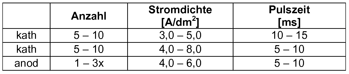
Pulsparameter (Fiq.71)Pulse parameter (Fiq.7 1 )
Stromdichte PulszeitCurrent-tight pulse time
Anzahl [A/dm2] [ms] kath 1 - 8 3,0 - 4,0 20 - 40 kath 1 - 8 4,0 - 6,0 10 - 15Number [A / dm 2 ] [ms] cath 1 - 8 3.0 - 4.0 20 - 40 cath 1 - 8 4.0 - 6.0 10 - 15
Pulsparameter (Fiα .8) :Pulse parameter (Fiα .8):
Stromdichte PulszeitCurrent-tight pulse time
Anzahl [A/dm2] [ms] kath 1 - 5 1,0 - 2,0 200 - 300 kath 120 - 200 1,0 - 2,0 5 - 10 kath 120 - 200 2,0 - 4,0 1 - 5 anod 2 - 10 1,5 - 3,0 150 - 250 kath 2 - 10 1,0 - 2,0 10 - 30 kath 1 - 5 1.0 - 2.0 2000 - 3000
Die jeweiligen Schichttypen zeigen dabei unterschiedliche Schichthärten; die Härte der Schichten ist abhängig vom Abscheideverfahren (alle Schichten wurden aus dem gleichen Bad abgeschieden) :Number [A / dm 2 ] [ms] cath 1 - 5 1.0 - 2.0 200 - 300 cath 120 - 200 1.0 - 2.0 5 - 10 cath 120 - 200 2.0 - 4.0 1 - 5 anod 2 - 10 1.5 - 3.0 150 - 250 cath 2 - 10 1.0 - 2.0 10 - 30 cath 1 - 5 1.0 - 2.0 2000 - 3000 The respective layer types show different layer hardnesses; the hardness of the layers depends on the deposition method (all layers were deposited from the same bath):
Typ Mikrohärte HV 0,1Type Microhardness HV 0.1
Kolumnar 220 - 250Columnar 220 - 250
Mischtyp 210 - 270 lamellar 420 - 460Mixed type 210 - 270 lamellar 420 - 460
Die in diesem Versuch mittels des erfindungsgemäßen Multipulsverfahrens hergestellten Nickelschichten weisen mit Abstand die höchste Mikrohärte auf.The nickel layers produced in this experiment by means of the multipulse method according to the invention have by far the highest microhardness.
Auch die generelle Schichtstruktur (kolumnar/feinkristallin/lamellar) kann erfindungsgemäß verändert werden. Hier spielt auch der anodische Anteil in der Abscheidesequenz eine wesentliche Rolle. Bei Veränderung des anliegenden Stroms durch beispielsweise Pulse kann sich die Art der adsorbierten Spezies ändern, und je nach Geschwindigkeitskonstante der Adsorption verändert sich dadurch die Oberflächendiffusion. Dies führt zu unterschiedlichen Kristallisationsmechanismen und Eigenschaften des abgeschiedenen Niederschlages.The general layer structure (columnar / fine-crystalline / lamellar) can also be changed according to the invention. Here too, the anodic portion plays an essential role in the deposition sequence. As the applied current is varied by, for example, pulses, the nature of the adsorbed species may change, and depending on the rate constant of the adsorption, the surface diffusion changes. This leads to different crystallization mechanisms and properties of the deposited precipitate.
Die Kinetik gleichzeitig ablaufender Reaktionen hat einen großen Einfluss auf die relative Geschwindigkeit konkurrierender Reaktionen, z.B. bei der Legierungsab- scheidung oder Wasserstoffentwicklung. Durch Beeinflussung der Abscheidungs- kinetik über die Form und Folge der angelegten Strompulse können Legierungszusammensetzungen und -phasen manipuliert und Nebenreaktionen unterdrückt werden. Bei der Reduktion des entstehenden Wasserstoff spielt auch die Pulspause eine wichtige Rolle. Während der Strompausen können adsorbierte Stoffe oder Gasbläschen desorbieren, insbesondere bei gleichzeitiger guter Badbewegung.The kinetics of concurrent reactions have a great influence on the relative rate of competing reactions, e.g. during alloying or hydrogen evolution. By influencing the deposition kinetics via the shape and sequence of the applied current pulses, alloy compositions and phases can be manipulated and side reactions suppressed. In the reduction of the resulting hydrogen and the pulse break plays an important role. During the pauses of the stream, adsorbed substances or gas bubbles can desorb, in particular with simultaneous good bath movement.
Bei der Herstellung mehrerer Schichten sind eventuell einfache oder mehrfache Spülschritte in Wasser angepasster Reinheit zwischen den einzelnen Schritten notwendig.In the production of multiple layers may be single or multiple rinses in water adjusted purity between steps necessary.
Alle zu beschichtenden Ausgangsmaterialen können in Vorbereitung einer galvanischen Beschichtung auf an sich bekannte Weise vorbehandelt bzw. aktiviert werden.All starting materials to be coated can be pretreated or activated in a manner known per se in preparation for a galvanic coating.
In den nachfolgenden Anwendungsbeispielen wurden folgende Elektrolytzusammensetzungen eingesetzt:
El:In the following application examples, the following electrolyte compositions were used: El:
Chemische Komponenten MenqeChemical components Menqe
Nickelsulfamat 70 - 90g/lNickel sulfamate 70 - 90g / l
Nickelbromid 5 - 20g/lNickel bromide 5 - 20g / l
Borsäure 30 - 40g/lBoric acid 30 - 40g / l
Org. Härtezusatz 15 - 25ml/lOrg. Hardness additive 15 - 25ml / l
Netzmittel 1 - 3ml/lWetting agent 1 - 3ml / l
Beispiel f. kommerzielles Bad: Enthone LectronicExample f. commercial bath: Enthone Lectronic
E2a: chemisches Nickelbad mit Phosphorgehalt 2 - 4% E2b: chemisches Nickelbad mit Phosphorgehalt 4 - 9% E2c: chemisches Nickelbad mit Phosphorgehalt 9 - 12%E2a: chemical nickel bath with phosphorus content 2 - 4% E2b: chemical nickel bath with phosphorus content 4 - 9% E2c: chemical nickel bath with phosphorus content 9 - 12%
E4:E4:
Chemische Komponenten MenqeChemical components Menqe
Nickelsulfat 230 - 300g/lNickel sulfate 230 - 300g / l
Nickelchlorid 40 - 60g/lNickel chloride 40 - 60g / l
Borsäure 30 - 40g/lBoric acid 30 - 40g / l
Netzmittel 2 - 3ml/lWetting agent 2 - 3ml / l
Org. Zusätze 20 - 30ml/lOrg. Additives 20 - 30ml / l
Beispiel f. kommerzielles Bad: Enthone Elpelyt E1 OXExample f. commercial bath: Enthone Elpelyt E1 OX
E5:E5:
Chemische Komponenten MenqeChemical components Menqe
Nickelsulfat 230 - 300g/lNickel sulfate 230 - 300g / l
Nickelchlorid 40 - 60g/lNickel chloride 40 - 60g / l
Borsäure 30 - 40g/lBoric acid 30 - 40g / l
Netzmittel 2 - 3ml/lWetting agent 2 - 3ml / l
Org. Glanzzusätze 20 - 30ml/lOrg. Shine additives 20 - 30ml / l
Beispiel f. kommerzielles Bad: Enthone Elpelyt GS6Example f. commercial bath: Enthone Elpelyt GS6
E6:E6:
Chemische Komponenten MengeChemical components quantity
Chromsäure 200 - 250g/lChromic acid 200 - 250g / l
Schwefelsäure 5 - 10g/lSulfuric acid 5 - 10g / l
Beispiel f. kommerzielles Bad: Metallchemie SaphirExample f. commercial bath: metal chemistry sapphire
E7:E7:
Chemische Komponenten MenqeChemical components Menqe
Chromsäure 280 - 300g/lChromic acid 280 - 300g / l
Schwefelsäure 3 - 6g/lSulfuric acid 3 - 6g / l
Netzmittel 5 - 10ml/lWetting agent 5 - 10ml / l
Beispiel f. kommerzielles Bad: Enthone Ankor 1120
E8:Example f. commercial bath: Enthone Ankor 1120 E8:
Chemische Komponenten MenqeChemical components Menqe
Silbercyanid 100 - 200g/lSilver cyanide 100-200g / l
Kaliumcyanid 50 - 150g/lPotassium cyanide 50 - 150g / l
Org. Zusätze 5 - 10ml/lOrg. Additives 5 - 10ml / l
Kaliumhydroxid 4g/lPotassium hydroxide 4g / l
Kaliumsilbercyanid 40 - 60g/lPotassium silver cyanide 40 - 60g / l
Beispiel f. kommerzielles Bad: Enthone SilvrexExample f. commercial bath: Enthone Silvrex
E9:E9:
Chemische Komponenten MenqeChemical components Menqe
Nickelsulfat 230 - 300g/lNickel sulfate 230 - 300g / l
Nickelchlorid 40 - 60g/lNickel chloride 40 - 60g / l
Borsäure 30 - 40g/lBoric acid 30 - 40g / l
Netzmittel 2 - 3ml/lWetting agent 2 - 3ml / l
Org. Zusätze 20 - 30ml/lOrg. Additives 20 - 30ml / l
Beispiel f. kommerzielles Bad: Metallchemie ORION 2100Example f. commercial bath: metal chemistry ORION 2100
ElO:ELO:
Chemische Komponenten MenqeChemical components Menqe
Kupfersulfat 70 - 90g/lCopper sulphate 70 - 90g / l
Beispiel f. kommerzielles Bad: Metallchemie CheluxExample f. commercial bath: metal chemistry Chelux
Anwendung 1:Application 1:
Zweck: Erhöhte Verschleißfestigkeit, überprüft im Testaufbau mit in einem befeuerten simulierten Motorlauf mit einem Mittel von 6.000 Umin - 1Purpose: Increased wear resistance, tested in test setup with in a simulated simulated engine run with a mean of 6,000 rpm
Status Quo: Haltbarkeit mit Gleichstromverfahren bzw. nur außenstromlosen Verfahren mit 4% Phosphor: 40 h, Härte herkömmlicher Schichten zwischen 250 - 800HVStatus quo: Durability with DC method or only electroless with 4% phosphorus: 40 h, hardness of conventional layers between 250 - 800HV
Erfindunαsαemäßes Verfahren : Haltbarkeit 250h, Oberflächenhärte ca. 600HV, Schichthärte ca. 1000HVInventive method: Shelf life 250h, surface hardness approx. 600HV, coating hardness approx. 1000HV
Substrat: Aluminiumleqierunq AISi20Fe5Ni2 Schichtsvstem :Substrate: Aluminum alloy AISi20Fe5Ni2 Layer system:

• Substratmaterial Aluminiumlegierung,Substrate material aluminum alloy,
• 2μm Sulfamatnickelschicht,2μm sulfamate nickel layer,
• 13μm chemisch Nickel,• 13μm chemical nickel,
• 2μm Sulfamatnickelschicht,2μm sulfamate nickel layer,
• 13μm chemisch Nickel,• 13μm chemical nickel,
• 2μm Nickel - Kobalt - Legierungsschicht• 2μm nickel - cobalt alloy layer
Beschichtunqsparameter: MP = Multipuls:Coating parameter: MP = Multipulse:

BP = bipolarer Puls:BP = bipolar pulse:

Anwendung 2:Application 2:
Zweck: Erhöhte thermische Verschleißfestigkeit von Aluminiumwerkstoffen Status Quo: Keine Haltbarkeit bei einer Dauerbelastung >100Purpose: Increased thermal resistance of aluminum materials Status Quo: No durability under continuous load> 100
Erfindunqsqemäßes Verfahren : Haltbarkeit über 250h bei Temperaturen bis 2000CInventive Method: Shelf life over 250 hours at temperatures up to 200 ° C.
Substrat: Aluminiumleαierunq AISi20Fe5Ni2 Schichtsvstem :Substrate: Aluminum alloy AISi20Fe5Ni2 Layer system:

MP = Multipuls:MP = Multipulse:

BP = bipolarer Puls:BP = bipolar pulse:

Anwendung 3:Application 3:
Zweck: zur gleichmäßigen verschleißfesten Beschichtung mit PartikeleinlagerungPurpose: for a uniform, wear-resistant coating with particle storage
Status Quo: Schichtdickenverteilung von bis zu 1 : 5 bei Verwendung von Gleichstromverfahren und gleichen Abscheidezeiten/SchichtdickenStatus Quo: Layer thickness distribution of up to 1: 5 when using DC methods and same deposition times / layer thicknesses
Erfindunαsαemäßes Verfahren : Schichtdickenverteilunαen bei 1 : 1,2Inventive Method: Layer thickness distributions at 1: 1.2
Substrat: WerkzeugstahlSubstrate: tool steel
Schichtsvstem :Schichtsvstem:

MP = Multipuls:MP = Multipulse:

BP = bipolarer Puls:BP = bipolar pulse:

Anwendung 4:Application 4:
Zweck: Schichtsystem mit schwingungsdämpfenden EigenschaftenPurpose: Layer system with vibration-damping properties
Status Quo: Keine beobachtbare Schwingungsdämpfende Wirkung bei Einsatz von Gleichstrom oder simplen Pulse/Pulse Reverse Plating Verfahren.Status Quo: No observable vibration damping effect when using DC or simple Pulse / Pulse reverse plating method.
Erfindunαsαemäßes Verfahren : Deutliche Schwingungsdämpfung kann auch bei zyklische Dauerbelastung beobachtet werden.Inventive Method: Significant vibration damping can be observed even with cyclic continuous loading.
Substrat: Aluminiumlegierung Schichtsvstem :Substrate: Aluminum Alloy Layer:

Fig. 11 : von links nach rechts:Fig. 11: from left to right:
• Substratmaterial Aluminiumlegierung,Substrate material aluminum alloy,
• 2μm Sulfamatnickelschicht,2μm sulfamate nickel layer,
• 13μm chemisch Nickel,• 13μm chemical nickel,
• 2μm Sulfamatnickelschicht,2μm sulfamate nickel layer,
• 13μm chemisch Nickel,
2μm Nickel - Kobalt - Legierungsschicht• 13μm chemical nickel, 2μm nickel - cobalt alloy layer
Beschichtunqsparameter:Beschichtunqsparameter:
MP = MultipulsMP = multipulse

BP = bipolarer Puls:BP = bipolar pulse:

Anwendung 5:Application 5:
Zweck: Herstellung korrosionsstabiler und verschleißfester Schichten Status Quo : Haltbarkeit im CASS Test (DIN 50021) < 24 StundenPurpose: To produce corrosion-resistant and wear-resistant coatings Status Quo: Durability in the CASS test (DIN 50021) <24 hours
Erfindunαsαemäßes Verfahren : Haltbarkeit des Schichtsystems >50 Stunden im CASS Test (DIN 50021) bei einer Schichthärte von ca. 1.000HVInventive method: Shelf life of the coating system> 50 hours in the CASS test (DIN 50021) with a layer hardness of approx. 1.000HV
Substrat: Stahl Schichtsvstem :Substrate: Steel Layer:

MP = Multipuls:MP = Multipulse:

SRP = superimposed reverse Puls:SRP = superimposed reverse pulse:
SP = superimposed Puls:SP = superimposed pulse:

Anwendung 6:Application 6:
Zweck: Herstellung von Schichten mit hoher thermischer ToleranzPurpose: To produce layers with high thermal tolerance
Status Quo: Abplatzen, Blasenbildung oder Rissbildung der über Gleichstrom/ außenstromlos aufgebrachten Schichtsysteme im Thermoschocktest: dreimaliger Zyklus Tempern bei 3000C für 2 Stunden gefolgt von Abschrecken in flüssigem Stickstoffe (<200°C).Status quo: Chipping, blistering or cracking of the DC / external electroless applied coating systems in the thermal shock test: three cycles annealing at 300 0 C for 2 hours followed by quenching in liquid nitrogen (<200 ° C).
Erfindunqsqemäßes Verfahren : Haltbarkeit des Schichtsystems im oben genannten Thermoschocktest ohne Auftreten von Blasen, Abplatzungen oder Rissbildungen.Inventive method: Shelf life of the layer system in the above-mentioned thermal shock test without occurrence of bubbles, flaking or cracking.
Substrat: Stahl Schichtsvstem :Substrate: Steel Layer:

MP = Multipuls:MP = Multipulse:

SRP = superimposed reverse Puls:SRP = superimposed reverse pulse:

SP = superimposed Puls:SP = superimposed pulse:

Anwendung 7:Application 7:
Zweck: Herstellung von Schichten mit hoher Korrosionsstabilität von Aluminium ThixogusslegierungenPurpose: To produce layers with high corrosion resistance of aluminum thixoglossal alloys
Status Quo: Beständigkeit im CASS - Test (DIN 50021) von herkömmlichen Gleichstrom oder außenstromlos - Nickel Schichten : 12hStatus Quo: Resistance in CASS test (DIN 50021) of conventional DC or external power - nickel layers: 12h
Erfindunqsqemäßes Verfahren : Beständigkeit im CASS - Test: 24h Substrat: Aluminiumlegierung AIMgSi7 Thixoguss Schichtsvstem :Inventive method: Resistance in the CASS test: 24 h Substrate: Aluminum alloy AIMgSi7 Thixoguss Schichtsvstem:

• Substratmaterial Aluminiumlegierung,Substrate material aluminum alloy,
• 10μm Sulfamatnickelschicht,• 10μm sulfamate nickel layer,
• 25μm chemisch Nickel,• 25μm chemical nickel,
• lOμm Halbglanznickelschicht,• 10 μm semi-bright nickel layer,
• lOμm Glanznickelschicht,• 10 μm bright nickel layer,
• 2μm Glanzchromschicht• 2μm gloss chrome layer
Beschichtunqsparameter: MP = Multipuls:Coating parameter: MP = Multipulse:

SRP = superimposed reverse Puls:SRP = superimposed reverse pulse:

SP = superimposed Puls:SP = superimposed pulse:

Anwendung 8:Application 8:
Zweck: Herstellung korrosionsbeständiger Sperrschichten bei hoher SchichtgleichmäßigkeitPurpose: To produce corrosion-resistant barrier layers with high layer uniformity
Status Quo: Ungenügende Diffusionssperrwirkung bzw. nur schlechte Schichtgleichmäßigkeit bei Verwendung von Gleichstromverfahren bzw. außenstromlosen VerfahrenStatus quo: Insufficient diffusion barrier effect or only poor layer uniformity when using DC methods or electroless methods
Erfindunqsqemäßes Verfahren : Ausgezeichnete Sperrwirkung auch bei thermischer Dauerbelastung bei 600C bei einer Schichtverteilung von 1 : 1,3Inventive method: Excellent barrier effect even under continuous thermal stress at 60 ° C. with a layer distribution of 1: 1.3
Substrat: Aluminiumlegierung
Schichtsvstem :Substrate: Aluminum alloy Schichtsvstem:

Beschichtunqsparameter:Beschichtunqsparameter:
MP = Multipuls:MP = Multipulse:

SPE = superimposed reverse Puls:SPE = superimposed reverse pulse:

SP = superimposed Puls:
 SP = superimposed pulse:
Anwendung 9:Application 9:
Zweck: Herstellung korrosionsbeständiger Sperrschichten bei hoher SchichtgleichmäßigkeitPurpose: To produce corrosion-resistant barrier layers with high layer uniformity
Status Quo : Ungenügende Diffusionssperrwirkung bzw. nur schlechte Schichtgleichmäßigkeit bei Verwendung von Gleichstromverfahren bzw. außenstromlosen VerfahrenStatus quo: Insufficient diffusion barrier effect or only poor layer uniformity when using DC methods or electroless methods
Erfindunqsqemäßes Verfahren : Ausgezeichnete Sperrwirkung auch bei thermischer Dauerbelastung bei 600C bei einer Schichtverteilung von 1 : 1,3
Substrat: AluminiumlegierungInventive method: Excellent barrier effect even under continuous thermal stress at 60 ° C. with a layer distribution of 1: 1.3 Substrate: Aluminum alloy
Schichtsvstem :Schichtsvstem:

Beschichtunqsparameter:Beschichtunqsparameter:
MP = Multipuls:MP = Multipulse:

SPE = superimposed reverse Puls:SPE = superimposed reverse pulse:

SP = superimposed Puls:SP = superimposed pulse:

Anwendung 10:Application 10:
Zweck: Herstellung korrosionsbeständiger Sperrschichten bei hoher SchichtgleichmäßigkeitPurpose: To produce corrosion-resistant barrier layers with high layer uniformity
Status Quo : Ungenügende Diffusionssperrwirkung bzw. nur schlechte Schichtgleichmäßigkeit bei Verwendung von Gleichstromverfahren bzw. außenstromlosen Verfahren
Erfindunqsqemäßes Verfahren : Ausgezeichnete Sperrwirkung auch bei thermischer Dauerbelastung bei 600C bei einer Schichtverteilung von 1 : 1,3Status quo: Insufficient diffusion barrier effect or only poor layer uniformity when using DC methods or electroless methods Inventive method: Excellent barrier effect even under continuous thermal stress at 60 ° C. with a layer distribution of 1: 1.3
Substrat: Aluminiumleqierunq Schichtsvstem :Substrate: Aluminum alloy coating system:

Beschichtunqsparameter:Beschichtunqsparameter:
MP = Multipuls:MP = Multipulse:

SPE = superimposed reverse Puls:SPE = superimposed reverse pulse:

SP = superimposed Puls:SP = superimposed pulse:

Anwendung 11:Application 11:
Zweck: Herstellung von Schichten mit hoher KorrosionsstabilitätPurpose: To produce layers with high corrosion resistance
Status Quo: Beständigkeit im CASS - Test (DIN 50021) von herkömmlichen Gleichstrom oder außenstromlos - Nickel Schichten : 12hStatus Quo: Resistance in CASS test (DIN 50021) of conventional DC or external power - nickel layers: 12h
Erfindunqsqemäßes Verfahren : Beständigkeit im CASS - Test (DIN 50021) : >24h
Substrat: Aluminiumlegierung AIMgSi7 Schichtsvstem :Inventive method: Resistance in the CASS test (DIN 50021):> 24 h Substrate: Aluminum Alloy AIMgSi7 Layer System:

Beschichtunqsparameter:Beschichtunqsparameter:
MP = Multipuls:MP = Multipulse:

BP = bipolarer Puls:BP = bipolar pulse:

SP = superimposed Puls:SP = superimposed pulse:

Anwendung 12:Application 12:
Zweck: Herstellung von Schichten mit hoher Korrosionsstabilität und Porenabdeckung des GrundsubstratsPurpose: To produce layers with high corrosion resistance and pore coverage of the base substrate
Status Quo: Beständigkeit im CASS - Test (DIN 50021) von herkömmlichen Gleichstrom oder außenstromlos - Nickel Schichten : 12hStatus Quo: Resistance in CASS test (DIN 50021) of conventional DC or external power - nickel layers: 12h
Erfindunαsαemäßes Verfahren : Beständigkeit im CASS - Test (DIN 50021) : >24h Substrat: Aluminiumlegierung AIMgSi7
Schichtsvstem :Inventive method: Resistance in the CASS test (DIN 50021):> 24 h Substrate: Aluminum alloy AIMgSi7 Schichtsvstem:

Beschichtunqsparameter:Beschichtunqsparameter:
MP = Multipuls:MP = Multipulse:

BP = bipolarer Puls:BP = bipolar pulse:

SP = superimposed Puls:
 SP = superimposed pulse:
Anwendung 13:Application 13:
Zweck: Herstellung von verschleißfesten Schichten auf AluminiumPurpose: To produce wear-resistant coatings on aluminum
Status Quo: Beständigkeit herkömmlicher außenstromlos oder Gleichstromverfahren im Tribotest < 100 StundenStatus Quo: Resistance of conventional external power or DC methods in the tribotest <100 hours
Erfindunqsqemäßes Verfahren : Beständigkeit im Tribotest > 200 Stunden Substrat: Aluminiumlegierungen
Schichtsvstem :Inventive method: Resistance in tribo test> 200 hours Substrate: Aluminum alloys Schichtsvstem:

Beschichtunqsparameter:Beschichtunqsparameter:
BP = bipolarer Puls:BP = bipolar pulse:

Claims
1. Elektrochemisches Beschichtungsverfahren für die Abscheidung von zumindest einer Schicht an zumindest einem Werkstück in einem Abscheidebad, mit zumindest eine Abscheidesequenz (P), die zumindest einmal wiederholt wird, wobei innerhalb der zumindest einen Abscheidesequenz (P) zumindest zwei Einzelsequenzen (A, B, C) vorgesehen sind, und jede Einzelsequenz (A, B, C) ein spezifisches Abscheidungsverfahren aufweist, dadurch gekennzeichnet, dass die zumindest zwei Einzelsequenzen (A, B, C) innerhalb einer Abscheidesequenz (P) unterschiedliche Abscheidungsverfahren aufweisen.1. An electrochemical coating method for the deposition of at least one layer on at least one workpiece in a deposition bath, comprising at least one deposition sequence (P) which is repeated at least once, wherein within the at least one deposition sequence (P) at least two individual sequences (A, B, C), and each individual sequence (A, B, C) has a specific deposition method, characterized in that the at least two individual sequences (A, B, C) have different deposition methods within a deposition sequence (P).
2. Beschichtungsverfahren nach Anspruch 1, dadurch gekennzeichnet, dass jede Einzelsequenzen (A, B, C) zumindest ein der nachfolgenden Abscheidungsverfahren umfasst:2. Coating process according to claim 1, characterized in that each individual sequence (A, B, C) comprises at least one of the following deposition processes:
• Gleichstrom• DC
• rein kathodische Pulse• purely cathodic pulses
• Kombination von kathodischen und anodischen Pulsen• Combination of cathodic and anodic pulses
• Kombination von kathodischen und anodischen Pulsen mit bis zu 500 Einzelpulsen• Combination of cathodic and anodic pulses with up to 500 single pulses
• Rampen - und/oder Dreieckspulse• Ramp and / or triangle pulses
• jedes der oben genannten Verfahren in Kombination mit einem Basisstrom• each of the above methods in combination with a base current
3. Beschichtungsverfahren nach Anspruch 1 oder 2, dadurch gekennzeichnet, dass zwischen zumindest zwei aufeinanderfolgenden Einzelsequenzen (A, B, C) und/oder nach Ablauf der zumindest einen Abscheidesequenz (P) eine Unterbrechung (D) des von außen zugeführten Stroms erfolgt.3. Coating method according to claim 1 or 2, characterized in that between at least two successive individual sequences (A, B, C) and / or after the expiry of the at least one deposition sequence (P) an interruption (D) of the externally supplied current takes place.
4. Beschichtungsverfahren nach einem der Ansprüche 1 bis 3, dadurch gekennzeichnet, dass eine Abscheidesequenz (P) zumindest eine Gleichstromabscheidung gefolgt von einer gepulsten Abscheidung aufweist.4. Coating method according to one of claims 1 to 3, characterized in that a deposition sequence (P) has at least one DC deposition followed by a pulsed deposition.
5. Beschichtungsverfahren nach einem der Ansprüche 2 bis 4, dadurch gekennzeichnet, dass der Basisstrom zwischen 1% und 75% der Abscheide- stromdichte aufweist.5. Coating method according to one of claims 2 to 4, characterized in that the base current between 1% and 75% of the deposition current density has.
6. Beschichtungsverfahren nach einem der Ansprüche 1 bis 5, dadurch gekennzeichnet, dass die Dauer einer Einzelsequenz (A, B, C) zwischen 1 und 3.000 ms beträgt. 6. Coating method according to one of claims 1 to 5, characterized in that the duration of a single sequence (A, B, C) is between 1 and 3,000 ms.
7. Beschichtungsverfahren nach einem der Ansprüche 1 bis 6, dadurch gekennzeichnet, dass das Abscheidebad zumindest eine wässrige Lösung zumindest eines Salzes oder Mischung von Salzen, zumindest eine Salzschmelze oder zumindest eine ionische Flüssigkeit oder Mischungen derselben enthält.7. Coating method according to one of claims 1 to 6, characterized in that the deposition bath contains at least one aqueous solution of at least one salt or mixture of salts, at least one molten salt or at least one ionic liquid or mixtures thereof.
8. Beschichtungsverfahren nach einem der Ansprüche 1 bis 7, dadurch gekennzeichnet, dass das Abscheidebad zusätzlich Feststoffe für den Einbau in die zumindest eine abgeschiedene Schicht enthält.8. Coating method according to one of claims 1 to 7, characterized in that the deposition bath additionally contains solids for incorporation into the at least one deposited layer.
9. Beschichtungsverfahren nach Anspruch 8, dadurch gekennzeichnet, dass die Feststoffe insbesondere Partikeln, Fasern, Flocken und/oder Nanotubes sind.9. Coating method according to claim 8, characterized in that the solids are in particular particles, fibers, flakes and / or nanotubes.
10. Elektrochemisches Beschichtungsverfahren für die Abscheidung einer Vielzahl von Schichten an zumindest einem Werkstück, dadurch gekennzeichnet, dass die Beschichtung zumindest vier Schichten aufweist.10. An electrochemical coating method for the deposition of a plurality of layers on at least one workpiece, characterized in that the coating has at least four layers.
11. Beschichtungsverfahren nach Anspruch 10, dadurch gekennzeichnet, dass die Schichten mit zumindest einem der nachfolgenden Verfahren aufgebracht werden :11. Coating method according to claim 10, characterized in that the layers are applied by at least one of the following methods:
• Gleichstrom• DC
• rein kathodische Pulse• purely cathodic pulses
• Kombination von kathodischen und anodischen Pulsen• Combination of cathodic and anodic pulses
• Kombination von kathodischen und anodischen Pulsen mit bis zu 500 Einzelpulsen• Combination of cathodic and anodic pulses with up to 500 single pulses
• Rampen - und/oder Dreieckspulse• Ramp and / or triangle pulses
• jedes der oben genannten Verfahren in Kombination mit einem Basisstrom• each of the above methods in combination with a base current
12. Beschichtungsverfahren nach Anspruch 10 oder 11, dadurch gekennzeichnet, dass zumindest zwei Schichten mit unterschiedlichen Verfahren aufgebracht werden.12. Coating method according to claim 10 or 11, characterized in that at least two layers are applied by different methods.
13. Elektrochemisches Beschichtungsverfahren für die Abscheidung einer Vielzahl von Schichten an zumindest einem Werkstück, wobei zumindest zwei Schichten mit unterschiedlichen Verfahren aufgebracht werden, dadurch gekennzeichnet, dass zumindest eine Schicht mit einem elektrochemischen Verfahren nach einem der Ansprüche 1 bis 9 aufgebracht wird. 13. An electrochemical coating method for the deposition of a plurality of layers on at least one workpiece, wherein at least two layers are applied by different methods, characterized in that at least one layer with an electrochemical method according to one of claims 1 to 9 is applied.
14. Beschichtungsverfahren nach Anspruch 13, dadurch gekennzeichnet, dass die Beschichtung zwei bis zwölf Schichten aufweist.14. Coating method according to claim 13, characterized in that the coating has two to twelve layers.
15. Beschichtungsverfahren nach Anspruch 13 oder 14, dadurch gekennzeichnet, dass auf eine erste, auf die Werkstückoberfläche aufgebrachte Primärschicht zumindest eine zweite Schicht folgt, die eine größere Schichtdicke als die Primärschicht aufweist.15. Coating method according to claim 13 or 14, characterized in that a first, applied to the workpiece surface primary layer at least a second layer follows, which has a greater layer thickness than the primary layer.
16. Beschichtungsverfahren nach Anspruch 15, dadurch gekennzeichnet, dass an die zweite Schicht zumindest eine dritte Abschlussschicht folgt, deren Schichtdicke geringer als jene der zweiten ist.16. Coating method according to claim 15, characterized in that the second layer is followed by at least one third end layer whose layer thickness is less than that of the second one.
17. Beschichtungsverfahren nach Anspruch 15 oder 16, dadurch gekennzeichnet, dass die zweite Schicht mittels eines stromlosen Verfahrens hergestellt ist.17. Coating process according to claim 15 or 16, characterized in that the second layer is produced by means of an electroless process.
18. Beschichtungsverfahren nach einem der Ansprüche 15 bis 17, dadurch gekennzeichnet, dass die Primärschicht und/oder die Abschlussschicht mittels des Verfahrens nach einem der Ansprüche 1 bis 9 hergestellt ist.18. Coating method according to one of claims 15 to 17, characterized in that the primary layer and / or the final layer by means of the method according to one of claims 1 to 9 is prepared.
19. Beschichtungsverfahren nach einem der Ansprüche 10 bis 18, dadurch gekennzeichnet, dass zwischen dem Aufbringen zweier Schichten eine thermische Behandlung erfolgt.19. Coating method according to one of claims 10 to 18, characterized in that a thermal treatment takes place between the application of two layers.
20. Beschichtungsverfahren nach einem der Ansprüche 10 bis 19, dadurch gekennzeichnet, dass zumindest eine Schicht mithilfe eines Plasmaoxidverfahrens aufgebracht wird.20. Coating method according to one of claims 10 to 19, characterized in that at least one layer is applied by means of a plasma oxide process.
21. Verwendung des Beschichtungsverfahrens nach einem der Ansprüche 1 bis 20 für die Abscheidung auf einem metallischen Werkstück oder einem nichtmetallischen Werkstück mit einem metallischen Überzug.21. Use of the coating method according to any one of claims 1 to 20 for the deposition on a metallic workpiece or a non-metallic workpiece with a metallic coating.
22. Verwendung nach Anspruch 21, dadurch gekennzeichnet, dass das Werkstück aus Aluminium, Magnesium oder Titan gefertigt ist.22. Use according to claim 21, characterized in that the workpiece is made of aluminum, magnesium or titanium.
2009 10 212009 10 21
Ha Ha
Priority Applications (1)
| Application Number | Priority Date | Filing Date | Title |
|---|---|---|---|
| EP09740674A EP2342371A2 (en) | 2008-10-23 | 2009-10-21 | Electrochemical coating method |
Applications Claiming Priority (2)
| Application Number | Priority Date | Filing Date | Title |
|---|---|---|---|
| ATA1661/2008 | 2008-10-23 | ||
| AT0166108A AT506583B9 (en) | 2008-10-23 | 2008-10-23 | ELECTROCHEMICAL COATING PROCESS |
Publications (2)
| Publication Number | Publication Date |
|---|---|
| WO2010046392A2 true WO2010046392A2 (en) | 2010-04-29 |
| WO2010046392A3 WO2010046392A3 (en) | 2010-07-15 |
Family
ID=41137170
Family Applications (1)
| Application Number | Title | Priority Date | Filing Date |
|---|---|---|---|
| PCT/EP2009/063793 WO2010046392A2 (en) | 2008-10-23 | 2009-10-21 | Electrochemical coating method |
Country Status (3)
| Country | Link |
|---|---|
| EP (1) | EP2342371A2 (en) |
| AT (1) | AT506583B9 (en) |
| WO (1) | WO2010046392A2 (en) |
Cited By (3)
| Publication number | Priority date | Publication date | Assignee | Title |
|---|---|---|---|---|
| EP3103897A1 (en) | 2015-06-11 | 2016-12-14 | ThyssenKrupp Steel Europe AG | Method for the electrochemical deposition of thin inorganic layers |
| WO2017045948A1 (en) | 2015-09-17 | 2017-03-23 | Robert Bosch Gmbh | Method for operating a battery cell |
| WO2017162235A1 (en) * | 2016-03-21 | 2017-09-28 | Allectra GmbH | Connecting element for gas-tight connection with other components for piping systems |
Citations (5)
| Publication number | Priority date | Publication date | Assignee | Title |
|---|---|---|---|---|
| US4869971A (en) | 1986-05-22 | 1989-09-26 | Nee Chin Cheng | Multilayer pulsed-current electrodeposition process |
| DE4009914A1 (en) | 1989-03-28 | 1990-10-18 | Usui Kokusai Sangyo Kk | HEAT AND CORROSION RESISTANT GALVANIC COATING |
| JP2000173949A (en) | 1998-12-09 | 2000-06-23 | Fujitsu Ltd | Semiconductor device, its manufacture, and plating method and device |
| CA2365749A1 (en) | 2001-12-20 | 2003-06-20 | The Governors Of The University Of Alberta | An electrodeposition process and a layered composite material produced thereby |
| EP1122989B1 (en) | 2000-02-01 | 2007-02-28 | Shinko Electric Industries Co. Ltd. | Method of plating for filling via holes |
Family Cites Families (5)
| Publication number | Priority date | Publication date | Assignee | Title |
|---|---|---|---|---|
| US4511438A (en) * | 1983-04-05 | 1985-04-16 | Harris Corporation | Bi-metallic electroforming technique |
| AU2002329410A1 (en) * | 2002-03-27 | 2003-10-13 | Isle Coat Limited | Process and device for forming ceramic coatings on metals and alloys, and coatings produced by this process |
| EP1526192A1 (en) * | 2003-10-24 | 2005-04-27 | Siemens Aktiengesellschaft | Electrolytic process for depositing a graded layer on a substrate and component |
| SE0403047D0 (en) * | 2004-12-14 | 2004-12-14 | Polymer Kompositer I Goeteborg | Pulse-plating method and apparatus |
| WO2006082218A1 (en) * | 2005-02-04 | 2006-08-10 | Siemens Aktiengesellschaft | Surface comprising a microstructure that reduces wettability and method for the production thereof |
-
2008
- 2008-10-23 AT AT0166108A patent/AT506583B9/en active
-
2009
- 2009-10-21 EP EP09740674A patent/EP2342371A2/en not_active Withdrawn
- 2009-10-21 WO PCT/EP2009/063793 patent/WO2010046392A2/en active Application Filing
Patent Citations (5)
| Publication number | Priority date | Publication date | Assignee | Title |
|---|---|---|---|---|
| US4869971A (en) | 1986-05-22 | 1989-09-26 | Nee Chin Cheng | Multilayer pulsed-current electrodeposition process |
| DE4009914A1 (en) | 1989-03-28 | 1990-10-18 | Usui Kokusai Sangyo Kk | HEAT AND CORROSION RESISTANT GALVANIC COATING |
| JP2000173949A (en) | 1998-12-09 | 2000-06-23 | Fujitsu Ltd | Semiconductor device, its manufacture, and plating method and device |
| EP1122989B1 (en) | 2000-02-01 | 2007-02-28 | Shinko Electric Industries Co. Ltd. | Method of plating for filling via holes |
| CA2365749A1 (en) | 2001-12-20 | 2003-06-20 | The Governors Of The University Of Alberta | An electrodeposition process and a layered composite material produced thereby |
Non-Patent Citations (1)
| Title |
|---|
| See also references of EP2342371A2 |
Cited By (4)
| Publication number | Priority date | Publication date | Assignee | Title |
|---|---|---|---|---|
| EP3103897A1 (en) | 2015-06-11 | 2016-12-14 | ThyssenKrupp Steel Europe AG | Method for the electrochemical deposition of thin inorganic layers |
| WO2017045948A1 (en) | 2015-09-17 | 2017-03-23 | Robert Bosch Gmbh | Method for operating a battery cell |
| DE102015217815A1 (en) | 2015-09-17 | 2017-03-23 | Robert Bosch Gmbh | Method for operating a battery cell |
| WO2017162235A1 (en) * | 2016-03-21 | 2017-09-28 | Allectra GmbH | Connecting element for gas-tight connection with other components for piping systems |
Also Published As
| Publication number | Publication date |
|---|---|
| WO2010046392A3 (en) | 2010-07-15 |
| AT506583B1 (en) | 2009-10-15 |
| EP2342371A2 (en) | 2011-07-13 |
| AT506583B9 (en) | 2009-12-15 |
| AT506583A4 (en) | 2009-10-15 |
Similar Documents
| Publication | Publication Date | Title |
|---|---|---|
| EP0862665B1 (en) | Process for the electrolytic deposition of metal layers | |
| EP2588645B1 (en) | Method for depositing a nickel-metal layer | |
| DE2462448A1 (en) | FLAT METAL OBJECT, PROCESS FOR ITS MANUFACTURING AND CATALYST FROM THIS METAL OBJECT | |
| EP1798313B1 (en) | Process for depositing crack-free, corrosion resistant and hard chromium and chromium alloy layers | |
| DE202016007550U1 (en) | Electroplated copper alloys with high strength and conductivity | |
| WO2021122106A1 (en) | Metal sheet having a deterministic surface structure and method for producing a formed and coated sheet-metal component | |
| EP1565596B1 (en) | Production of structured hard chrome layers | |
| AT506583B9 (en) | ELECTROCHEMICAL COATING PROCESS | |
| EP2212447A2 (en) | Gold-containing nickel layer | |
| DE10013298C2 (en) | Method for applying a metal layer on light metal surfaces and application of the method | |
| DE10146559A1 (en) | Process for the deposition of a zinc-nickel alloy from an electrolyte | |
| EP4010515A1 (en) | Method and system for electrolytically coating an electrically conductive strip and/or woven material by means of pulse technology | |
| WO2013164165A1 (en) | Multi-layer surface coating having chrome cover layer without nickel layer | |
| EP3517655A1 (en) | Method for black chromium plating | |
| DE10060127B4 (en) | Electrolytic iron deposition bath and method for electrodepositing iron and applications of the method | |
| EP1433879B1 (en) | Process for metal surface coating with an alkali phosphate solution, aqueous concentrate and use of such coated metal surfaces | |
| WO2022112379A1 (en) | Ruthenium alloy layer and its layer combinations | |
| DE3821402A1 (en) | IMPROVED ELECTROGALVANIZED COATING FOR STEEL | |
| EP2975162A1 (en) | Method for providing a workpiece with a protective coating | |
| AT412880B (en) | PROCESS FOR COATING A WORKPIECE OF TITANIUM OR A TITANIUM ALLOY WITH A FUNCTIONAL LAYER | |
| WO2011036260A2 (en) | Method for galvanization and passivation | |
| DE2165329A1 (en) | Fast nickel plating - using a nickel salt acid electrolyte | |
| JPH09316682A (en) | Zinc-nickel base alloy electroplated steel sheet and its production | |
| DE102009041250A1 (en) | Process for the electrolytic copper plating of zinc die casting with reduced tendency to blister |
Legal Events
| Date | Code | Title | Description |
|---|---|---|---|
| 121 | Ep: the epo has been informed by wipo that ep was designated in this application |
Ref document number: 09740674 Country of ref document: EP Kind code of ref document: A2 |
|
| NENP | Non-entry into the national phase |
Ref country code: DE |
|
| REEP | Request for entry into the european phase |
Ref document number: 2009740674 Country of ref document: EP |
|
| WWE | Wipo information: entry into national phase |
Ref document number: 2009740674 Country of ref document: EP |