WO2010044444A1 - 巡回型a/d変換器、イメージセンサデバイス、及びアナログ信号からディジタル信号を生成する方法 - Google Patents
巡回型a/d変換器、イメージセンサデバイス、及びアナログ信号からディジタル信号を生成する方法 Download PDFInfo
- Publication number
- WO2010044444A1 WO2010044444A1 PCT/JP2009/067853 JP2009067853W WO2010044444A1 WO 2010044444 A1 WO2010044444 A1 WO 2010044444A1 JP 2009067853 W JP2009067853 W JP 2009067853W WO 2010044444 A1 WO2010044444 A1 WO 2010044444A1
- Authority
- WO
- WIPO (PCT)
- Prior art keywords
- signal
- circuit
- output
- value
- capacitors
- Prior art date
- Legal status (The legal status is an assumption and is not a legal conclusion. Google has not performed a legal analysis and makes no representation as to the accuracy of the status listed.)
- Ceased
Links
Images




Classifications
-
- H—ELECTRICITY
- H03—ELECTRONIC CIRCUITRY
- H03M—CODING; DECODING; CODE CONVERSION IN GENERAL
- H03M1/00—Analogue/digital conversion; Digital/analogue conversion
- H03M1/06—Continuously compensating for, or preventing, undesired influence of physical parameters
- H03M1/0617—Continuously compensating for, or preventing, undesired influence of physical parameters characterised by the use of methods or means not specific to a particular type of detrimental influence
- H03M1/0675—Continuously compensating for, or preventing, undesired influence of physical parameters characterised by the use of methods or means not specific to a particular type of detrimental influence using redundancy
- H03M1/069—Continuously compensating for, or preventing, undesired influence of physical parameters characterised by the use of methods or means not specific to a particular type of detrimental influence using redundancy by range overlap between successive stages or steps
- H03M1/0695—Continuously compensating for, or preventing, undesired influence of physical parameters characterised by the use of methods or means not specific to a particular type of detrimental influence using redundancy by range overlap between successive stages or steps using less than the maximum number of output states per stage or step, e.g. 1.5 per stage or less than 1.5 bit per stage type
-
- H—ELECTRICITY
- H03—ELECTRONIC CIRCUITRY
- H03M—CODING; DECODING; CODE CONVERSION IN GENERAL
- H03M1/00—Analogue/digital conversion; Digital/analogue conversion
- H03M1/12—Analogue/digital converters
- H03M1/14—Conversion in steps with each step involving the same or a different conversion means and delivering more than one bit
-
- H—ELECTRICITY
- H03—ELECTRONIC CIRCUITRY
- H03M—CODING; DECODING; CODE CONVERSION IN GENERAL
- H03M1/00—Analogue/digital conversion; Digital/analogue conversion
- H03M1/12—Analogue/digital converters
-
- H—ELECTRICITY
- H04—ELECTRIC COMMUNICATION TECHNIQUE
- H04N—PICTORIAL COMMUNICATION, e.g. TELEVISION
- H04N25/00—Circuitry of solid-state image sensors [SSIS]; Control thereof
- H04N25/70—SSIS architectures; Circuits associated therewith
- H04N25/76—Addressed sensors, e.g. MOS or CMOS sensors
- H04N25/77—Pixel circuitry, e.g. memories, A/D converters, pixel amplifiers, shared circuits or shared components
-
- H—ELECTRICITY
- H03—ELECTRONIC CIRCUITRY
- H03M—CODING; DECODING; CODE CONVERSION IN GENERAL
- H03M1/00—Analogue/digital conversion; Digital/analogue conversion
- H03M1/12—Analogue/digital converters
- H03M1/1205—Multiplexed conversion systems
- H03M1/123—Simultaneous, i.e. using one converter per channel but with common control or reference circuits for multiple converters
-
- H—ELECTRICITY
- H03—ELECTRONIC CIRCUITRY
- H03M—CODING; DECODING; CODE CONVERSION IN GENERAL
- H03M1/00—Analogue/digital conversion; Digital/analogue conversion
- H03M1/12—Analogue/digital converters
- H03M1/34—Analogue value compared with reference values
- H03M1/38—Analogue value compared with reference values sequentially only, e.g. successive approximation type
- H03M1/40—Analogue value compared with reference values sequentially only, e.g. successive approximation type recirculation type
- H03M1/403—Analogue value compared with reference values sequentially only, e.g. successive approximation type recirculation type using switched capacitors
-
- H—ELECTRICITY
- H04—ELECTRIC COMMUNICATION TECHNIQUE
- H04N—PICTORIAL COMMUNICATION, e.g. TELEVISION
- H04N25/00—Circuitry of solid-state image sensors [SSIS]; Control thereof
- H04N25/60—Noise processing, e.g. detecting, correcting, reducing or removing noise
- H04N25/67—Noise processing, e.g. detecting, correcting, reducing or removing noise applied to fixed-pattern noise, e.g. non-uniformity of response
- H04N25/671—Noise processing, e.g. detecting, correcting, reducing or removing noise applied to fixed-pattern noise, e.g. non-uniformity of response for non-uniformity detection or correction
- H04N25/677—Noise processing, e.g. detecting, correcting, reducing or removing noise applied to fixed-pattern noise, e.g. non-uniformity of response for non-uniformity detection or correction for reducing the column or line fixed pattern noise
Definitions
- the present invention relates to a cyclic A / D converter, an image sensor device, and a method for generating a digital signal from an analog signal.
- Patent Document 1 describes an A / D conversion array.
- the A / D conversion circuit of the A / D conversion array includes two capacitors and an inverting amplifier.
- the DA converter of the A / D converter circuit provides one of the three values (V RM , V RP , GND) to one capacitor.
- Patent Document 2 describes a cyclic A / D converter.
- the cyclic A / D converter includes two pairs of capacitors and an amplifier having a differential input and a differential output.
- the DA conversion unit of the A / D converter provides one of three values (V RM , V RP , COMMON) to the pair of capacitors.
- Patent Document 3 describes a high-accuracy cyclic A / D converter.
- the A / D converter includes three capacitors and a differential input operational amplifier.
- the DA converter of the A / D converter provides any one of three values (+ V R , ⁇ V R , GND) to a predetermined capacitor among the three.
- Patent Document 4 describes a cyclic A / D converter.
- the A / D converter includes two pairs of capacitors and an amplifier having a differential input and a differential output.
- the DA converter of the A / D converter provides one of three values (+ V ref1 , ⁇ V ref2 , COMMON) to the pair of capacitors.
- Patent Document 5 describes an N-bit A / D converter. This A / D converter includes two pairs of capacitors and an operational amplifier circuit.
- the DA conversion circuit of the A / D converter provides one of three values (+ V R , ⁇ V R , GND) to the pair of capacitors.
- Patent Document 6 describes an analog-digital converter. This analog-digital converter includes four capacitors and an operational amplifier circuit. The DA conversion circuit of the A / D converter provides one of three values (V REFP , V REFN , COMMON) to the pair of capacitors.
- Patent Document 7 describes an A / D converter. This A / D converter includes two capacitors and an operational amplifier circuit. The DA conversion circuit of the A / D converter provides any one of three values (V RM , V RP , COMMON) to the pair of capacitors.
- Each of the A / D converters of Patent Documents 1 to 7 uses a gain stage including a single operational amplifier circuit and a plurality of capacitors.
- the gain stage circuit has either a single-ended configuration or a differential amplification configuration.
- the differential amplification type gain stage requires twice as many capacitors as the single-ended type gain stage.
- the cyclic operation of the single-ended gain stage requires the above three values (V RM , V RP , zero) reference voltage. This reference voltage is provided by the DA conversion circuit of the A / D converter.
- the circuit area of the single-end type gain stage is smaller than the circuit area of the differential amplification type gain stage.
- one of three reference voltages is provided to one end of a capacitor in the gain stage for D / A conversion.
- these reference voltages are not generated accurately, an error occurs in the A / D conversion, and the linearity of the A / D conversion characteristic is impaired.
- it is not easy to generate the reference voltage accurately.
- a circuit using resistance voltage division is used to generate a reference voltage, the accuracy of the resistance ratio in the semiconductor integrated circuit is not high.
- it is used for trimming of a resistance value. The use of trimming not only increases the area of the A / D converter but also requires adjustment of the trimming value of the A / D converter.
- An object of the present invention is made in view of such circumstances, and an object of the present invention is to provide a cyclic A / D converter that can reduce the number of reference voltages for D / A conversion.
- An object of the present invention is to provide an image sensor device including this cyclic A / D converter, and further to provide a method for generating a digital signal from an analog signal, which can reduce the number of reference voltages for D / A conversion. The purpose is to do.
- the cyclic A / D converter includes (a) an input that receives an analog signal to be converted into a digital value, an output, and a single-ended operational amplifier circuit having a first input, a second input, and an output.
- a gain stage (b) an A / D conversion circuit that generates a digital signal including a plurality of bits according to a signal from the output of the gain stage or the analog signal; and (c) first to second signals according to the digital signal.
- a logic circuit that generates a control signal having a value of 3, and (d) a D / A conversion circuit that provides at least one of the first and second voltage signals to the gain stage in response to the control signal. .
- the gain stage includes first to third capacitors.
- a second input of the operational amplifier circuit receives a reference potential, and the gain stage generates an arithmetic value by the operational amplifier circuit and the first to third capacitors, and the arithmetic value is output to the first and second capacitors.
- a storing operation is performed for storing in the capacitor, and the D / A conversion circuit has first and second outputs connected to the first and second capacitors, respectively.
- the third capacitor is connected between the output of the operational amplifier circuit and the first input, and the first and second capacitors are connected between the D / A conversion circuit and the first input. Then, the calculated value is generated at the output of the gain stage.
- the D / A conversion circuit provides either the first or second voltage signal to the first output and one of the first or second voltage signal to the second output. Including a switch circuit.
- the first and second capacitors are connected to the first and second outputs of the D / A conversion circuit, respectively, and the switch of the D / A conversion circuit
- the circuit can provide at least one of the first and second voltage signals to the first output and provide at least one of the first and second voltage signals to the second output. it can. Therefore, in the calculation operation, by switching the first and second voltage signals to one end of the first and second capacitors by using the switch circuit, the gain stage causes the three voltage signals from the D / A conversion circuit. Behaves as received.
- the switch circuit supplies the first voltage signal to both the first and second capacitors in response to the first value of the control signal. And supplying first and second voltage signals to the first and second capacitors, respectively, in response to the second value of the control signal, and in response to the third value of the control signal.
- the second voltage signal is supplied to both the first and second capacitors.
- the first and second voltage signals of the D / A conversion circuit are provided to the first and second capacitors, respectively, the first and second voltage signals are the first and second voltage signals. Synthesized via the first and second capacitors.
- the switch circuit includes a first switch connected between the first voltage signal source and the first output, and the second voltage signal.
- a second switch connected between the source and the second output, and a third switch connected between the first output and the second output.
- the D / A converter circuit turns on the first switch and the third switch in response to the first value of the control signal, thereby causing the first output and the second output, respectively.
- the first voltage signal is supplied to the first capacitor and the second capacitor via the first and second capacitors.
- the D / A conversion circuit turns on the first switch in response to the second value of the control signal, thereby causing the first capacitor to pass through the first output.
- the second voltage signal is supplied to the second capacitor via the second output by turning on the second switch.
- the D / A conversion circuit turns on the second switch and the third switch in response to the third value of the control signal, thereby causing the first output and the second output, respectively.
- the second voltage signal is supplied to the first capacitor and the second capacitor through the first and second capacitors.
- the first and second capacitors are used.
- the third voltage value is synthesized from the voltage signal.
- the third capacitor in the storing operation, is connected between the output of the operational amplifier circuit and the first input, and the first and second capacitors are operated and amplified. It can be connected between the output of the circuit and a reference potential. According to this cyclic A / D converter, signals for the next cyclic A / D conversion are stored in the first and second capacitors.
- the gain stage can further perform an initial reset operation.
- the first to third capacitors are connected between the first input of the operational amplifier circuit and the output of the operational amplifier circuit, and the first input of the operational amplifier circuit is connected to the operational amplifier circuit. Can be connected to the output.
- the initial reset operation of the first to third capacitors can be performed using the operational amplifier circuit.
- the gain stage in the initial storage operation, connects the first input of the operational amplifier circuit and the output of the operational amplifier circuit to each other and transmits the analog signal to the first to second analog signals. 3 capacitor.
- an analog signal can be stored in the first to third capacitors as an initial storing operation.
- This image sensor device includes (a) a cell array including an array of image sensor cells, and (b) a converter array connected to the cell array and including a plurality of cyclic A / D converters.
- Each of the cyclic A / D converters is connected to the image sensor cell via a column line of the cell array, and each of the cyclic A / D converters is as described above.
- each of the cyclic A / D converters uses a D / A conversion circuit that provides at least one of the first and second voltage signals to the gain stage. Therefore, the area of the image sensor device can be reduced.
- the image sensor cell can generate the first signal indicating the reset level and the second signal indicating the signal level superimposed on the reset level.
- the gain stage is connected to the output of the operational amplifier circuit and the first input, and the first and second capacitors are connected between the input of the gain stage and the first input of the operational amplifier circuit to reset the gain stage.
- a level signal is received by the first and second capacitors.
- the gain stage connects the third capacitor between the output of the operational amplifier circuit and the first input, and between the first input of the gain stage and the first input of the operational amplifier circuit.
- the first and second capacitors receive a signal level signal connected to the capacitor.
- the reset level by the reset operation can be canceled from the second signal using the gain stage.
- the image sensor device can further include a noise cancellation circuit.
- the image sensor cell includes a first signal including a first redundant bit example indicating a reset level and a second signal including a second redundant bit example indicating a signal level superimposed on the reset level.
- the noise cancellation circuit can generate a first storage circuit that stores a first A / D conversion value of the signal at the reset level, and a second A / D conversion value of the signal at the signal level.
- a second storage circuit to store, a difference between the first A / D conversion value and the second A / D conversion value is generated, and the reset level is subtracted from the second signal to generate reset noise.
- an arithmetic circuit to be canceled According to this image sensor device, the reset level by the reset operation can be canceled from the second signal by using the digital signals of the first and second signals from the image sensor cell.
- the arithmetic circuit converts the first redundant bit string (first signal) and the second redundant bit string (second signal) into non-redundant bit strings, respectively.
- a second redundant-nonredundant counter circuit, a complement, and an adder, and a difference between an output value of the first redundant-nonredundant conversion circuit and an output value of the second redundant-nonredundant conversion circuit is a noise cancellation value Can be output as According to this image sensor device, the difference between the output value of the first redundant-nonredundant conversion circuit and the output value of the second redundant-nonredundant conversion circuit can be generated using a complementer and an adder.
- An image sensor device is connected to a first reference voltage circuit that generates a first voltage signal, a second reference voltage circuit that generates a second voltage signal, and the first reference voltage circuit.
- the first conductive line and a second conductive line connected to the second reference voltage circuit can be further provided.
- the D / A conversion circuit in each cyclic A / D converter is connected to the first and second conductive lines. According to this image sensor device, two conductive lines are used instead of three to provide the first and second voltage signals to each cyclic A / D converter.
- Yet another aspect of the present invention is a method for generating a digital signal from an analog signal using cyclic A / D conversion.
- the method includes (a) storing an A signal having an analog value in first to third capacitors, and (b) representing a digital value of the A signal, and any one of the first to third values.
- a D 0 signal having, after generating (c) D 0 signal, the first and with connecting third capacitor between the first input and output operational amplifier circuit of the operational amplifier circuit
- the output of the operational amplifier circuit (D) storing the calculated values in the first and second capacitors and generating a Di signal having the first to third values and representing the digital value of the calculated value
- the D / A signal is either the first or second voltage signal having an analog value corresponding to the D 0 signal or the D i signal.
- the D 0 signal When the D 0 signal has the first value, the first voltage signal Is added to the other end of the first capacitor and the other end of the second capacitor, and when the D 0 signal is a second value, the second voltage signal is applied to the other end of the first capacitor and the second capacitor. It was added to the other end, when D 0 signal is the third value, the first and second voltage signals, respectively, are applied to the other ends of the first and second capacitors.
- the D i signal When the D i signal has the first value, the first voltage signal is applied to the other end of the first capacitor and the other end of the second capacitor, and the D i signal has the second value.
- the first and second voltage signals are respectively Added to the other ends of the first and second capacitors.
- the second input of the operational amplifier circuit receives a reference potential.
- an analog signal when performing cyclic A / D conversion, can be received using two voltage signals without using three voltage signals, and a digital signal representing the analog signal can be generated. .
- a cyclic A / D converter that can reduce the number of reference voltages for D / A conversion is provided.
- an image sensor device including the cyclic A / D converter is provided.
- a method for generating a digital signal from an analog signal that can reduce the number of reference voltages for D / A conversion.
- FIG. 1 is a diagram showing a circuit block of a cyclic A / D converter according to the present embodiment.
- FIG. 2 is a diagram showing the relationship between the calculated value V OP and the digital value for each round.
- FIG. 3 is a diagram showing clock timings in the cyclic A / D converter shown in FIG.
- FIG. 4 is a diagram showing an operation of the cyclic A / D converter shown in FIG.
- FIG. 5 is a diagram showing circuit connections for the initial reset operation.
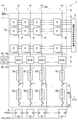
- FIG. 6 is a diagram illustrating a circuit block of the image sensor device.
- FIG. 7 is a diagram illustrating pixels of the image sensor.
- FIG. 8 is a block diagram showing an arithmetic circuit in the digital noise cancellation circuit.
- FIG. 9 is a diagram showing a circuit block of a cyclic A / D converter according to the present embodiment.
- FIG. 10 shows the main steps for analog CDS.
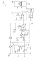
- FIG. 1 is a diagram showing a circuit block of a cyclic A / D converter according to the present embodiment.
- the cyclic A / D converter 11 includes a gain stage 15, an A / D conversion circuit 17, a logic circuit 19, and a D / A conversion circuit 21.
- the gain stage 15 includes an input 15a for receiving the analog signal V IN to be converted to a digital value, and an output 15b to provide a calculation value V OP of each one cyclic.
- the gain stage 15 includes a single-ended operational amplifier circuit 23 and first to third capacitors 25, 27, and 29.
- the operational amplifier circuit 23 has a first input 23a, an output 23b, and a second input 23c.
- the phase of the signal of the output 23b is inverted from the phase of the signal applied to the first input 23a.
- the first and second inputs 23a and 23c are an inverting input terminal and a non-inverting input terminal, respectively, and the output 23b is a non-inverting output terminal.
- a second input 23c of the operational amplifier circuit 23 is connected to a reference potential line L COM, also receives a reference voltage V COM.
- the A / D conversion circuit 17 generates a digital signal D according to the signal V OP or the analog signal VIN from the output 23b of the gain stage 23.
- the A / D conversion circuit 17 can include, for example, two comparators 17a and 17b.
- the comparators 17a and 17b respectively compare the input analog signal with respective predetermined reference signals V RCH and V RCL and provide comparison result signals B0 and B1 as shown in FIG.
- the reference signals V RCH and V RCL in the A / D conversion circuit 17 are provided by voltage sources 37a and 37b, respectively.
- the digital signal D indicates an A / D conversion value for each round.
- the digital signal D has, for example, 2 bits (B 0 , B 1 ), and each bit (B 0 , B 1 ) can take “1” or “0”.
- the logic circuit 19 generates a control signal V CONT (for example, ⁇ DH , ⁇ DL , ⁇ DS ) corresponding to the digital signal D.
- V CONT for example, ⁇ DH , ⁇ DL , ⁇ DS
- the A / D conversion circuit 17 uses, for example, one comparator in a time division manner to compare the operation value VOP with the reference signal and to provide signals B0 and B1 indicating the comparison result. it can.
- the gain stage 15 can include arithmetic operations and storage operations.
- the calculation value V OP is generated by the calculation amplifier circuit 23 and the first to third capacitors 25, 27, and 29.
- the calculated value V OP is stored in the first and second capacitors 25 and 27.
- the first and second capacitors 25 and 27 are connected to the first and second outputs 21a and 21b of the D / A conversion circuit, respectively.
- the switch circuit 31 of the D / A conversion circuit 21 can provide at least one of the voltage signals V DA1 and V DA2 to the first output 21a in response to the control signal V CONT , and the voltage signal V DA1 , At least one of V DA2 can be provided to the second output 21b. Therefore, in the calculation operation, the gain stage 15 is switched from the D / A conversion circuit 21 to three types by applying the voltage signals V DA1 and V DA2 to one end of the capacitors 25 and 27 by using the switch circuit 31. Operates like receiving a voltage signal.
- FIG. 2 is a diagram showing conversion characteristics between the calculated value V OP and the digital value for each round.
- V OP range D 0, V RCL > V OP ,
- D 1, V RCH ⁇ V OP ⁇ V RCL ,
- D 2, V OP > V RCH , (1) It becomes.
- the A / D conversion circuit 17 compares the calculated value VOP from the gain stage 15 with two predetermined reference signals to generate a ternary redundant digital signal.
- the D / A conversion circuit 21 provides at least one of the first and second voltage signals V RH and V RL to the gain stage 15 in response to the control signal V CONT .
- the D / A conversion circuit 21 includes first and second outputs 21 a and 21 b and a switch circuit 31.
- the switch circuit 31 provides either the first or second voltage signal V RH or V RL to the first output 21 a and the first and second voltages to the second output 21 b.
- One of the two voltage signals V RH and V RL is provided.
- the voltage signals V RH and V RL are provided by the first and second voltage sources 33 and 35.
- the first voltage source 33 provides a voltage VRH .
- the second voltage source 35 provides the voltage VRL .
- the output 33 a of the first voltage source 33 is connected to the output 21 a through the switch 31 a in the switch circuit 31 and is connected to the output 21 b through the switches 31 a and 31 c in the switch circuit 31.
- the output 35 a of the second voltage source 35 is connected to the output 21 a via the switches 31 b and 31 c in the switch circuit 31 and is connected to the output 21 b via the switch 31 b in the switch circuit 31.
- the first and second outputs 21a and 21b of the D / A conversion circuit 21 are connected to one ends 25a and 27a of the first and second capacitors 25 and 27, respectively. Since the opening and closing of the switches 31a to 31c are controlled by control signals ⁇ DH , ⁇ DS , ⁇ DL from the logic circuit 17, the values of the digital signals B 1, B 0 are the control signals ⁇ DH , ⁇ DS , ⁇ DL, respectively. Determine which of these will be active.
- the D / A conversion circuit 21 provides a value as shown in FIG.
- condition D 0 is satisfied,
- the gain stage 15 includes a plurality of switches for connecting the capacitors 25, 27 and 29 and the operational amplifier circuit 23. Although these switches are shown in FIG. 1, the arrangement of the switches 43, 47, 49, 51, 53, 55 is an example. These switches 43, 47, 49, 51, 53, 55 are controlled by the clock generator 41.
- FIG. 3 is a diagram showing clock timings in the cyclic A / D converter shown in FIG.
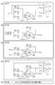
- FIG. 4 explains the operation of the cyclic A / D converter shown in FIG.
- Capacitors 25, 27 and 29 have capacitances C 1a , C 1b and C 2 , respectively.
- step S101 (and S201) in FIG. 4A an initial storage operation is performed.
- the analog signal VIN is stored in the capacitors 25, 27, and 29. Capacitors 25, 27 and 29 are connected in parallel to each other for storage. Further, the initial analog signal VIN is provided to the A / D conversion circuit 17.
- the cyclic A / D converter 11 includes first switch means for storing the analog signal VIN in the capacitors 25, 27, and 29. The first analog signal VIN is supplied to the A / D conversion circuit 17 by the first switch means.
- the A / D conversion circuit 17 generates a digital signal D1 (1) (D2 (1)).
- the signal D1 (1) is provided to the logic circuit 19, and the logic circuit 19 generates a control signal V CONT that controls the D / A conversion circuit 21.
- the terminal 25a of the capacitor 25 is connected to the input 15a via the switch 43, and the terminal 27a of the capacitor 27 is connected to the input 15a via the switches 31c, 43.
- the terminal 29a of the capacitor 29 is connected to the input 15a via the switches 43 and 51, and the reference potential is supplied to the terminals 25b and 27b of the capacitors 25 and 27 via the switches 49 and 53.
- a reference potential is supplied to 29b via a switch 53.
- the terminal 29a and the output 23b of the capacitor 29 are separated by the switch 55, and the output 23b is separated from the input 15a by the switch 55.
- the A / D conversion circuit 17 receives the original analog signal VIN and generates a digital signal D (1) in response to the clock ⁇ c.
- the terminal 25a of the capacitor 25 and the terminal 27a of the capacitor 27 are connected via the switch 31c, a separate switch can be provided for this connection.
- signals ( ⁇ DH , ⁇ DL , ⁇ DS ) indicate waveforms for controlling the D / A conversion circuit 21 for the sake of simplicity.
- the signal ( ⁇ DS ) includes a signal waveform for connection between the terminal 25a of the capacitor 25 and the terminal 27a of the capacitor 27, in addition to the signal waveform of the control.
- step S102 (and S202) of FIG. 4B and FIG. 4C a calculation operation is performed.
- the gain stage 15 generates the arithmetic value V OP by the operational amplifier circuit 23 and the capacitors 25, 27, and 29.
- the capacitor 29 is connected between the output 15b and the input 15a of the operational amplifier circuit 15, and the capacitors 25 and 27 are connected between the D / A conversion circuit 21 and the input 23a.
- the cyclic A / D converter 11 includes a second switch means for an arithmetic operation.
- the D / A conversion circuit 21 provides the voltage signal V DA1 and / or V DA2 to the gain stage 15.
- V OP (1 + C 1 / C 2 ) ⁇ V IN ⁇ V R (3)
- C 1 C 1a + C 1b (4) It is.
- the deviation of the absolute values of the reference voltages V RH and V RL does not affect the linearity of the A / D conversion characteristics, and only the accuracy of generating the midpoint voltage affects the linearity.
- the capacitance ratio accuracy of the capacitor defines this midpoint voltage.
- the specific accuracy of the capacitance is much higher than the specific accuracy of the resistor, and a highly accurate A / D converter 11 can be provided.
- step S103 (and S203) of FIG. 4D a storing operation is performed.
- the calculated value V OP on the output 23 b of the operational amplifier circuit 23 is stored in the first and second capacitors 25 and 27.
- Capacitors 25 and 27 are connected in parallel to each other for storage.
- Cyclic A / D converter 11 includes third switch means for storing operation value VOP . Further, the operation value V OP is provided to the A / D conversion circuit 17 as an analog signal by the third switch means.
- the terminal 25a of the capacitor 25 is connected to the output 23b via the switches 51 and 55, and the terminal 27a of the capacitor 27 is output via the switches 31c, 51 and 55.
- the reference potential is supplied to the terminals 25 b and 27 b of the capacitors 25 and 27 through the switch 47.
- the terminals 25a and 27a of the capacitors 25 and 27 are separated from the input 15a by the switch 43, and the terminals 25b and 27b of the capacitors 25 and 27 are separated from the input 23a by the switch 49.
- the input 23a of the operational amplifier circuit 23 becomes the reference potential VCOM .
- the operation value V OP is provided to the A / D conversion circuit 17 by the third switch means (in this embodiment, the switch 55).
- step S104 (S204) of FIG. 4E steps S102 (S202) and S103 (S203) are repeated to generate digital signals D1 (2) to D1 (N) and D2 (2) to D2 (N). To do. This repetition is performed until an A / D conversion result having a predetermined number of bits is obtained. For example, if N cycles are performed, a resolution corresponding to approximately N + 1 bits can be obtained.
- step S105 an initial reset operation is performed in step S105 (and S205) in FIG.
- both ends of the capacitors 25, 27, and 29 are connected.
- a reference potential V COM is applied to both ends of the capacitors 25, 27, and 29 for later operation.
- the gain stage 15 connects the capacitors 25, 27, and 29 between the input 23a and the output 23b of the operational amplifier circuit 23, and connects the input 23a of the operational amplifier circuit 23 to the output 23b.
- a reference potential VCOM is generated at the output 23c of the operational amplifier circuit 23.
- V RCH and V RCL are given by, for example, equations (8) and (9).
- V RCH (3 ⁇ V RH + 5 ⁇ V RL ) / 8
- V RCL (5 ⁇ V RH + 3 ⁇ V RL ) / 8 (9)
- the conversion characteristics per cycle represented by the equations (1), (2), (8), and (9) are shown in FIG.
- FIG. 6 is a diagram illustrating a circuit block of the image sensor device.
- a vertical shift register 3 is connected to a row of a cell array 2 including an array of image sensor cells 2a, and an A / D converter array 4 is connected to a column of the cell array 2.
- the A / D converter array 4 includes a plurality of A / D converters arranged in an array.
- An A / D converter 11 can be used as each A / D converter.
- Each of the A / D converters 11 is connected to the image sensor cell 2 a via the column line 8.
- a bias circuit 9 is connected to the column line 8, and the bias circuit 9 includes a current source transistor 9 a and a current source I bias provided in each column line 8.
- the A / D conversion values (D1 (1) to D1 (N)) of the signal S1 at the reset level and the A / D conversion values (D2) of the signal S2 at the signal level. (1) to D2 (N)) are generated.
- each cyclic A / D converter 11 uses a D / A conversion circuit 21 for the gain stage 15. Therefore, the area of the image sensor device 1 can be reduced.
- the output of the A / D converter array 4 is converted into an M-bit digital code corresponding to the signal from the pixel 2a by the redundant expression-non-redundant expression conversion circuit 7.
- the image sensor device 1 includes a reference voltage circuit 33 for generating a RH voltage signal V, a reference voltage circuit 35 for generating a voltage signal V RL, a first conductive line 10a connected to the reference voltage circuit 33, the reference voltage And a conductive line 10b connected to the circuit 35.
- the conductive lines 10a and 10b extend in a direction crossing the direction in which the column line 8 extends.
- the D / A conversion circuit 21 in each cyclic A / D converter 11 is connected to the conductive lines 10a and 10b. According to this image sensor device, in order to provide the reference voltage signals V RH and V RL to the cyclic A / D converter 11, two conductive lines 10 a and 10 b are used instead of three.
- FIG. 7 is a diagram illustrating pixels of the image sensor.
- the pixel 2a has, for example, a CMOS image sensor cell structure.
- the photodiode DF receives light L for one pixel related to the image.
- the gate of the selection transistor M S is connected to the row select line S extending in the row direction.
- the gate of the reset transistor M R is connected to the reset line R.
- the gate of the transfer transistor M T is connected to the transfer selection line extending in the row direction.
- One end of the photodiode DF is connected to the floating diffusion layer FD via the transfer transistor M T.
- Floating diffusion layer FD is connected to a reset potential line Reset via the reset transistor M R, is connected to the gate of the transistor M A.
- One current terminal (for example, drain) of the transistor M A is connected to the column line 8 via the selection transistor M S.
- Transistor M A is provided in the column line through the selection transistor M S a potential corresponding to the charge amount of the floating
- the noise canceling operation is performed as follows. First, to provide a reset control signal R to the reset transistor M R, it resets the floating diffusion layer FD. Through the amplification transistor M A, read out the reset level. Then, a charge transfer control signal TX is supplied to the transfer transistor M T, is transferred from the photodiode DF photoinduced signal charges to the floating diffusion layer. Thereafter, through the transistor M A, reading the signal level. As described above, the pixel 2a can generate the signal S1 indicating the reset level and the signal S2 indicating the signal level superimposed on the reset level.
- the difference between the reset level and the signal level is obtained by the digital noise cancellation circuit 5.
- noises such as fixed pattern noise due to variations in the transistor characteristics of the pixel 2a and reset noise generated when the floating diffusion layer is reset are canceled.
- a noise cancellation circuit 5 is connected to the A / D converter array 4, and an output of the A / D converter array 4 is provided to the noise cancellation circuit 5.
- An A / D conversion value corresponding to the signal from the pixel 2 a is stored in the noise cancellation circuit 5.
- the noise cancellation circuit 5 provides the digital signal D OUT to the output of the image sensor 1.
- Digital noise cancellation is performed by obtaining a difference between a bit string indicating the signal S1 indicating the reset level and a bit string indicating the signal S2 indicating the signal level superimposed on the reset level.
- the noise cancellation circuit 5 includes a first storage circuit 61, a second storage circuit 63, and an arithmetic circuit 65.
- the first storage circuit 61 stores A / D conversion values (D1 (1) to D1 (N)) generated according to the timing chart of FIG.
- the second storage circuit 63 stores A / D conversion values (D2 (1) to D2 (N)) generated according to the timing chart of FIG.
- the arithmetic circuit 65 calculates the difference between the bit strings stored in the two storage circuits 61 and 63, thereby generating the output V OUT from which digital noise has been canceled.
- D (1) is It is the most significant bit
- D (N) is the least significant bit
- each output value D (i ⁇ 1) (B0 (i ⁇ 1), B1 (i ⁇ 1)) is expressed.
- a bit string for each digit is generated from the sequence of A / D conversion output values.
- the B0 bit string is expressed as (B0 (1), B0 (2),..., B0 (N)), and the B1 bit string is (B1 (0), B1 (2),..., B1 (N)). It is expressed.
- Conversion from a redundant code to a non-redundant code is performed as follows.
- D, B1, B0 for ternary redundant code D 0, 0, 0 1, 0, 1 2, 1, 1
- the non-redundant code is an N + 1 digit binary number obtained by adding an N digit B0 bit string to an N digit B1 bit string.
- Represented by The above addition is performed by an adder.
- one of these non-redundant codes is converted into a complement expression, and subtraction is performed by an adder. Thereby, noise cancellation is performed.
- FIG. 8 is a block diagram showing an arithmetic circuit in the digital noise cancellation circuit.
- the redundant bit string at the reset level from the A / D converter array 4 is stored in the storage circuit 73.
- the storage circuit 73 includes a B0 bit string storage circuit 73a and a B1 bit string storage circuit 73b.
- the storage circuit 73 is connected to the redundant-nonredundant conversion circuit 77.
- the adder 77a of the redundant-nonredundant conversion circuit 77 converts the digital value of the N-bit redundant expression into the digital value D N + 1 (R) of the N + 1-bit nonredundant expression.
- the redundant bit string of the signal level from the A / D converter array 4 is stored in the storage circuit 75.
- the storage circuit 75 includes a B0 bit string storage circuit 75a and a B1 bit string storage circuit 75b.
- the storage circuit 75 is connected to the redundant-nonredundant conversion circuit 79.
- the adder 79a of the redundant-nonredundant conversion circuit 79 converts the digital value of the N-bit redundant expression into the digital value D N + 1 (S) of the N + 1-bit nonredundant expression.
- the redundant-nonredundant conversion circuit 79 is connected to a complementer 81, and the complementer 81 generates a nonredundant complement representation digital value (N + 1 bit nonredundant complement representation digital value) D N + 1 (S).
- the adder 83 adds the digital value D N + 1 (R) and the digital value D N + 1 (S) to generate a digital value V OUT whose noise has been canceled.
- the reset level noise due to the reset operation is generated from the charge indicating the reset noise and the charge indicating the received light amount. Cancel from the signal.
- redundant-non-redundant conversion circuits 77 and 79 can be included in the storage circuits 61 and 63 shown in FIG. 6, respectively.
- Redundant-nonredundant conversion circuits 77 and 79 may include storage circuits 77b and 79b for storing digital values of N + 1 bit nonredundant expressions, respectively.
- the storage circuit 63 can include a complement 81.
- the arithmetic circuit 65 can include an adder 83. According to this configuration, a digital value of non-redundant expression is generated in a circuit provided for each column, and the arithmetic circuit 65 is shared by all columns.
- the redundant-nonredundant conversion circuits 77 and 79 and the complementer 81 can be included in the arithmetic circuit 65 shown in FIG.
- the arithmetic circuit 65 receives the digital values of two N-bit redundant representations respectively shown in the signals S1 and S2, performs a redundant-nonredundant conversion on these, and generates a difference value. According to this configuration, the redundant-nonredundant conversion circuit and the differentiator are shared for all the columns.
- the difference between the reset level and the signal level can be canceled during A / D conversion.
- This cancels noise such as fixed pattern noise due to variations in the transistor characteristics of the pixel 2a and reset noise generated when the floating diffusion layer is reset.
- FIG. 9 is a diagram showing a circuit block of the cyclic A / D converter according to the present embodiment.
- the cyclic A / D converter 11 a includes a gain stage 15, an A / D conversion circuit 17, a logic circuit 19, and a D / A conversion circuit 21.
- the gain stage 15 includes an input 15a for receiving the analog signal V IN to be converted to a digital value, and an output 15b to provide a calculation value V OP of each one cyclic.
- the gain stage 15 includes a single-ended operational amplifier circuit 23 and first to third capacitors 25, 27, and 29.
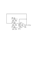
- FIG. 10 is a diagram illustrating the main steps for analog correlated double sampling (CDS).
- CDS analog correlated double sampling
- the terminals 25a and 27a of the capacitors 25 and 27 are connected to the input 15a, and a reference potential is supplied to the terminals 25b and 27b of the capacitors 25 and 27.
- the reference potential V COM is generated at the output 23 c of the operational amplifier circuit 23.
- the capacitors 25 and 27 receive the signal S1 indicating the reset level.
- Capacitors 25 and 27 are connected in parallel to each other for storage.
- the capacitors 25 and 27 receive the signal S2 indicating the signal level.
- the cyclic A / D converter 11a stores the signal S2 in the capacitors 25 and 27 and generates a difference between the signal S1 and the signal S2.
- the difference value is stored in the capacitors 25, 27, and 29 for subsequent cyclic operations.
- the cyclic A / D converter 11a includes sixth switch means for generating a difference between the signal S1 and the signal S2.
- capacitors 25 and 27 connected in parallel are connected between the input 15a and the input 23a of the operational amplifier circuit 23, and the capacitor 29 is connected to the input 23a and the output of the operational amplifier circuit 23. 23b.
- the gain stage 15 connects the input 23 a and the output 23 c of the operational amplifier circuit 23 to each other, the operational value V OP is generated at the output 23 c of the operational amplifier circuit 23.
- the gain stage 15 is used to A / D convert a signal that cancels the reset level due to the reset operation. This A / D conversion is performed by the steps shown in FIGS. 4B to 4D.
Landscapes
- Engineering & Computer Science (AREA)
- Theoretical Computer Science (AREA)
- Multimedia (AREA)
- Signal Processing (AREA)
- Analogue/Digital Conversion (AREA)
Abstract
Description
特許文献2には、巡回型A/D変換器が記載されている。この巡回型A/D変換器は、2対のキャパシタと、差動入力及び差動出力を有する増幅器とを含む。A/D変換器のDA変換部は、3値(VRM、VRP、COMMON)のいずれかを一対のキャパシタに提供する。
特許文献3には、高精度巡回型A/D変換器が記載されている。このA/D変換器は、3つのキャパシタと、差動入力オペアンプとを含む。A/D変換器のDA変換部は、3値(+VR、-VR、GND)のいずれかを3つのうちの所定のキャパシタに提供する。
特許文献4には、巡回型A/D変換器が記載されている。このA/D変換器は、2対のキャパシタと、差動入力及び差動出力を有する増幅器とを含む。A/D変換器のDA変換部は、3値(+Vref1、-Vref2、COMMON)のいずれかを一対のキャパシタに提供する。
特許文献5には、NビットA/D変換器が記載されている。このA/D変換器は、2対のキャパシタと、演算増幅回路とを含む。A/D変換器のDA変換回路は、3値(+VR、-VR、GND)のいずれかを一対のキャパシタに提供する。
特許文献6には、アナログディジタル変換器が記載されている。このアナログディジタル変換器は、4つのキャパシタと、演算増幅回路とを含む。A/D変換器のDA変換回路は、3値(VREFP、VREFN、COMMON)のいずれかを一対のキャパシタに提供する。
特許文献7には、A/D変換器が記載されている。このA/D変換器は、2つのキャパシタと、演算増幅回路とを含む。A/D変換器のDA変換回路は、3値(VRM、VRP、COMMON)のいずれかを一対のキャパシタに提供する。
方法が提供される。
ディジタル信号 演算値VOPの範囲
D=0のとき、VRCL>VOP、
D=1のとき、VRCH≧VOP≧VRCL、
D=2のとき、VOP>VRCH、 (1)
となる。A/D変換回路17がゲインステージ15からの演算値VOPを所定の2つの基準信号と比較することによって3値の冗長ディジタル信号を生成している。
条件D=2が満たされるとき、VDA1=VDA2=VRHを提供する。
条件D=1が満たされるとき、VDA1=VRH、VDA2=VRLを提供する。
条件D=0が満たされるとき、
VDA1=VDA2=VRLを提供する。 (2)
演算値VOPは以下の式で表される。
VOP=(1+C1/C2)×VIN-VR (3)
C1=C1a+C1b (4)
である。また、値VRはD/A変換回路21からの電圧信号VDA1、VDA2によって規定されており、以下のように表される。
条件D=2が満たされるとき、VR=(C1a+C1b)×VRH/C2である。
条件D=1が満たされるとき、VR=(C1a×VRH+C1b×VRL)/C2である。
条件D=0が満たされるとき、
VR=(C1a+C1b)×VRL/C2である。 (5)
VOP=2×VIN-VR (6)
また、関係(3)も以下のように書き換えられる。
条件D=2が満たされるとき、VR=VRHである。
条件D=1が満たされるとき、VR=(VRH+VRL)/2である。
条件D=0が満たされるとき、
VR=VRLである。 (7)
すなわち、D/A変換回路21は、3値のA/D変換値に対してVRH、VRL又はその中点の電圧(VRH+VRL)/2の3値を生成する。3値の生成が2つの参照電源のみを用いて可能にされるので、参照電圧源の数及び参照電圧の提供する配線の領域を節約できる。
る。
VRCH=(3×VRH+5×VRL)/8 (8)
VRCL=(5×VRH+3×VRL)/8 (9)
式(1)、(2)、(8)、(9)で表される1巡回あたりの変換特性は、図2に示される。
D、B1、B0
0、 0、 0
1、 0、 1
2、 1、 1
という対応により、A/D変換回路17の出力B1、B0の値が規定されるとき、非冗長コードは、N桁のB0ビット列をN桁のB1ビット列と加算して得られるN+1桁の2進数によって表される。上記の加算は加算器で行われる。リセットレベル及び信号レベルの各々のA/D変換値を非冗長コードに変換し後に、これらの非冗長コードの一方を補数表現に変換して、加算器により減算を行う。これにより、ノイズキャンセルが行われる。
出力15bを含む。また、ゲインステージ15は、シングルエンド型の演算増幅回路23及び第1~第3のキャパシタ25、27、29を含む。
タ25、27に格納するための第5のスイッチ手段を含む。
VOP=(C1a+C1b)/C2×(VR-VS)
で表される。
Claims (12)
- 巡回型A/D変換器であって、
ディジタル値に変換されるアナログ信号を受ける入力、出力、並びに第1の入力、第2の入力及び出力を有するシングルエンド型の演算増幅回路を含むゲインステージと、
前記ゲインステージの前記出力からの信号又は前記アナログ信号に応じて、複数ビットを含むディジタル信号を生成するA/D変換回路と、
前記ディジタル信号に応じて、第1~第3の値を有する制御信号を生成する論理回路と、
前記制御信号に応答して前記ゲインステージに第1及び第2の電圧信号の少なくともいずれか一方を提供するD/A変換回路と
を備え、
前記ゲインステージは、第1~第3のキャパシタを含み、
前記演算増幅回路の前記第2の入力は、基準電位を受け、
前記ゲインステージは、前記演算増幅回路及び前記第1~第3のキャパシタにより演算値を生成する演算動作と、該演算値を前記第1及び第2のキャパシタに格納する格納動作を行い、
前記D/A変換回路は、前記第1及び第2のキャパシタにそれぞれ接続された第1及び第2の出力を有しており、
前記演算動作では、前記第3のキャパシタが前記演算増幅回路の前記出力と前記第1の入力との間に接続されると共に前記第1及び第2のキャパシタが前記D/A変換回路と前記第1の入力との間に接続されて、前記演算値が当該ゲインステージの前記出力に生成され、
前記D/A変換回路は、前記制御信号に応答して、前記第1の出力に前記第1及び第2の電圧信号のいずれかを提供すると共に前記第2の出力に前記第1及び第2の電圧信号のいずれかを提供するためのスイッチ回路を含む、ことを特徴とする巡回型A/D変換器。 - 前記スイッチ回路は、前記制御信号の前記第1の値に応答して、前記第1及び第2のキャパシタの両方に前記第1の電圧信号を供給し、前記制御信号の前記第2の値に応答して、前記第1及び第2のキャパシタにそれぞれ第1及び第2の電圧信号を供給し、前記制御信号の前記第3の値に応答して、前記第1及び第2のキャパシタの両方に前記第2の電圧信号を供給する、ことを特徴とする請求項1に記載された巡回型A/D変換器。
- 前記スイッチ回路は、前記第1の電圧信号源と前記第1の出力との間に接続された第1のスイッチと、前記第2の電圧信号源と前記第2の出力との間に接続された第2のスイッチと、並びに前記第1の出力と前記第2の出力との間に接続された第3のスイッチとから構成され、
前記D/A変換回路は、前記制御信号の前記第1の値に応答して、前記第1のスイッチ及び前記第3のスイッチをオンすることにより、それぞれ前記第1の出力、第2の出力を介して前記第1のキャパシタ及び第2のキャパシタに前記第1の電圧信号を供給し、
前記D/A変換回路は、前記制御信号の前記第2の値に応答して、前記第1のスイッチをオンすることにより、前記第1の出力を介して前記第1のキャパシタに前記第1の電圧信号を供給すると共に、前記第2のスイッチをオンすることにより、前記第2の出力を介して前記第2のキャパシタに前記第2の電圧信号を供給し、
前記D/A変換回路は、前記制御信号の前記第3の値に応答して、前記第2のスイッチ及び前記第3のスイッチをオンすることにより、それぞれ前記第1の出力、第2の出力を介して前記第1のキャパシタ及び第2のキャパシタに前記第2の電圧信号を供給する、ことを特徴とする請求項1又は請求項2に記載された巡回型A/D変換器。 - 前記格納動作では、前記第3のキャパシタが前記演算増幅回路の前記出力と前記第1の入力との間に接続されると共に前記第1及び第2のキャパシタが前記演算増幅回路の前記出力と前記基準電位との間に接続される、ことを特徴とする請求項1~請求項3のいずれか一項に記載された巡回型A/D変換器。
- 前記ゲインステージは、さらに、初期リセット動作を行うことができ、
前記初期リセット動作では、前記第1~第3のキャパシタは、前記演算増幅回路の前記第1の入力と前記演算増幅回路の前記出力との間に接続されると共に、前記演算増幅回路の前記第1の入力が前記演算増幅回路の前記出力に接続される、ことを特徴とする請求項1~請求項4のいずれか一項に記載された巡回型A/D変換器。 - 前記ゲインステージは、初期格納動作では、前記演算増幅回路の前記第1の入力と前記演算増幅回路の前記出力とを互いに接続すると共に、前記アナログ信号を前記第1~第3のキャパシタに受ける、ことを特徴とする請求項1~請求項5のいずれか一項に記載された巡回型A/D変換器。
- イメージセンサデバイスであって、
イメージセンサセルのアレイを含むセルアレイと、
前記セルアレイに接続されており複数の巡回型A/D変換器を含む変換器アレイと
を備え、
前記巡回型A/D変換器の各々は、前記セルアレイのカラム線を介して前記イメージセンサセルに接続されており、
前記巡回型A/D変換器の各々は請求項1~請求項6のいずれか一項に記載されたものである、ことを特徴とするイメージセンサデバイス。 - 前記イメージセンサセルは、リセットレベルを示す第1の信号と該リセットレベルに重畳された信号レベルを示す第2の信号とを生成可能であり、
前記ゲインステージは、前記演算増幅回路の前記出力と前記第1の入力とを互いに接続すると共に、前記ゲインステージの前記入力と前記演算増幅回路の前記第1の入力との間に前記第1及び第2のキャパシタを接続して、前記リセットレベルの信号を前記第1及び第2のキャパシタに受けており、
前記ゲインステージは、前記第3のキャパシタを前記演算増幅回路の前記出力と前記第1の入力との間に接続すると共に、前記ゲインステージの前記入力と前記演算増幅回路の前記第1の入力との間に接続して、前記信号レベルの信号を前記第1及び第2のキャパシタに受けている、ことを特徴とする請求項7に記載されたイメージセンサデバイス。 - ノイズキャンセル回路を更に備え、
前記イメージセンサセルは、リセットレベルを示す、第1の冗長ビット例からなる第1の信号と該リセットレベルに重畳された信号レベルを示す、第2の冗長ビット例からなる第2の信号とを生成可能であり、
前記ノイズキャンセル回路は、前記リセットレベルの信号の第1のA/D変換値を格納する第1の記憶回路と、前記信号レベルの信号の第2のA/D変換値を格納する第2の記憶回路と、前記第1のA/D変換値と前記第2のA/D変換値との差を生成して前記第2の信号から該リセットレベルを差し引いてリセットノイズをキャンセルする演算回路とを含む、ことを特徴とする請求項7に記載されたイメージセンサデバイス。 - 前記演算回路は、前記第1及び第2の冗長ビット列を第1及び第2の非冗長ビット列にそれぞれ変換する第1及び第2冗長-非冗長反感回路、補数器、並びに加算器を含み、
前記演算回路は、前記第1冗長-非冗長変換回路の出力値と前記第2冗長-非冗長変換回路の出力値との差分をノイズキャンセル値として出力する、ことを特徴とする請求項9に記載されたイメージセンサデバイス。 - 前記第1の電圧信号を発生する第1の基準電圧回路と、
前記第2の電圧信号を発生する第2の基準電圧回路と、
前記第1の基準電圧回路に接続された第1の導電線と、
前記第2の基準電圧回路に接続された第2の導電線と
を更に備え、
各巡回型A/D変換器内の前記D/A変換回路は、前記第1及び第2の導電線に接続されている、ことを特徴とする請求項7~請求項10のいずれか一項に記載されたイメージセンサデバイス。 - 巡回型A/D変換を用いてアナログ信号からディジタル信号を生成する方法であって、
(a)第1~第3のキャパシタにアナログ値を有するA信号を格納するステップと、
(b)前記A信号のディジタル値を表しており第1~第3の値のいずれかを有するD0信号を生成するステップと、
(c)前記D0信号を生成した後に、前記第3のキャパシタを演算増幅回路の出力と演算増幅回路の第1の入力との間に接続すると共に前記第1及び第2のキャパシタの一端を前記演算増幅回路の前記第1の入力に接続して、前記第1のキャパシタの他端及び前記第2のキャパシタの他端にD/A信号を加えることによって、前記演算増幅回路の前記出力に演算値を生成するステップと、
(d)前記第1及び第2のキャパシタに前記演算値を格納すると共に、前記演算値のディジタル値を表しており第1~第3の値を有するDi信号を生成するステップと、
(e)ステップ(c)及び(d)を繰り返して、前記ディジタル信号を生成するステップと
を備え、
前記D/A信号は、前記D0信号又は前記Di信号に応じたアナログ値の第1及び第2の電圧信号の少なくともいずれかであり、
前記D0信号が前記第1の値であるとき、前記第1の電圧信号が前記第1のキャパシタの他端及び前記第2のキャパシタの他端に加えられ、
前記D0信号が前記第2の値であるとき、前記第2の電圧信号が前記第1のキャパシタの他端及び前記第2のキャパシタの他端に加えられ、
前記D0信号が前記第3の値であるとき、前記第1及び第2の電圧信号が、それぞれ、前記第1及び第2のキャパシタの他端に加えられ、
前記Di信号が前記第1の値であるとき、前記第1の電圧信号が前記第1のキャパシタの他端及び前記第2のキャパシタの他端に加えられ、
前記Di信号が前記第2の値であるとき、前記第2の電圧信号が前記第1のキャパシタの他端及び前記第2のキャパシタの他端に加えられ、
前記Di信号が前記第3の値であるとき、前記第1及び第2の電圧信号が、それぞれ、前記第1及び第2のキャパシタの他端に加えられる、ことを特徴とする方法。
Priority Applications (3)
| Application Number | Priority Date | Filing Date | Title |
|---|---|---|---|
| US13/124,319 US8581171B2 (en) | 2008-10-17 | 2009-10-15 | Cyclic A/D converter, image sensor device, and method for generating digital signal from analog signal |
| CN200980141382.7A CN102187581B (zh) | 2008-10-17 | 2009-10-15 | 循环型a/d转换器、图像传感器装置及从模拟信号生成数字信号的方法 |
| JP2010533923A JP5187782B2 (ja) | 2008-10-17 | 2009-10-15 | 巡回型a/d変換器、イメージセンサデバイス、及びアナログ信号からディジタル信号を生成する方法 |
Applications Claiming Priority (2)
| Application Number | Priority Date | Filing Date | Title |
|---|---|---|---|
| JP2008-269001 | 2008-10-17 | ||
| JP2008269001 | 2008-10-17 |
Publications (1)
| Publication Number | Publication Date |
|---|---|
| WO2010044444A1 true WO2010044444A1 (ja) | 2010-04-22 |
Family
ID=42106608
Family Applications (1)
| Application Number | Title | Priority Date | Filing Date |
|---|---|---|---|
| PCT/JP2009/067853 Ceased WO2010044444A1 (ja) | 2008-10-17 | 2009-10-15 | 巡回型a/d変換器、イメージセンサデバイス、及びアナログ信号からディジタル信号を生成する方法 |
Country Status (5)
| Country | Link |
|---|---|
| US (1) | US8581171B2 (ja) |
| JP (1) | JP5187782B2 (ja) |
| KR (1) | KR101545769B1 (ja) |
| CN (1) | CN102187581B (ja) |
| WO (1) | WO2010044444A1 (ja) |
Cited By (2)
| Publication number | Priority date | Publication date | Assignee | Title |
|---|---|---|---|---|
| KR20130093489A (ko) * | 2010-05-14 | 2013-08-22 | 고쿠리츠 다이가꾸 호우진 시즈오까 다이가꾸 | A/d 변환기 |
| US9380235B2 (en) | 2014-03-14 | 2016-06-28 | Kabushiki Kaisha Toshiba | AD conversion circuit |
Families Citing this family (2)
| Publication number | Priority date | Publication date | Assignee | Title |
|---|---|---|---|---|
| WO2010044444A1 (ja) * | 2008-10-17 | 2010-04-22 | 国立大学法人静岡大学 | 巡回型a/d変換器、イメージセンサデバイス、及びアナログ信号からディジタル信号を生成する方法 |
| KR102795751B1 (ko) * | 2019-05-21 | 2025-04-15 | 삼성전자주식회사 | 아날로그-디지털 변환을 수행하는 전단 회로 및 이를 포함하는 터치 처리 회로 |
Citations (2)
| Publication number | Priority date | Publication date | Assignee | Title |
|---|---|---|---|---|
| JPS6256023A (ja) * | 1985-09-02 | 1987-03-11 | Fujitsu Ltd | A/d変換器 |
| JP2008141399A (ja) * | 2006-11-30 | 2008-06-19 | National Univ Corp Shizuoka Univ | Nビットa/d変換器 |
Family Cites Families (9)
| Publication number | Priority date | Publication date | Assignee | Title |
|---|---|---|---|---|
| JP3962788B2 (ja) | 2003-10-29 | 2007-08-22 | 国立大学法人静岡大学 | A/d変換アレイ及びイメージセンサ |
| JP4469988B2 (ja) | 2005-09-07 | 2010-06-02 | 国立大学法人静岡大学 | ノイズキャンセル機能付きa/d変換器 |
| JP4478798B2 (ja) | 2005-10-07 | 2010-06-09 | 国立大学法人静岡大学 | オフセット低減機能をもつ巡回型a/d変換器、およびオフセット電圧を低減する方法 |
| JP4482694B2 (ja) | 2006-02-03 | 2010-06-16 | 国立大学法人静岡大学 | 高精度巡回型a/d変換器とこれを用いたイメージセンサ |
| JP4423427B2 (ja) | 2006-11-30 | 2010-03-03 | 国立大学法人静岡大学 | アナログディジタル変換器およびイメージセンシング半導体デバイス |
| JP4328863B2 (ja) | 2006-11-30 | 2009-09-09 | 国立大学法人静岡大学 | 巡回型a/d変換器およびイメージセンサ |
| US7443333B2 (en) | 2007-02-13 | 2008-10-28 | Freescale Semiconductor, Inc. | Single stage cyclic analog to digital converter with variable resolution |
| WO2009088041A1 (ja) * | 2008-01-09 | 2009-07-16 | National University Corporation Shizuoka University | 巡回型アナログ・ディジタル変換器 |
| WO2010044444A1 (ja) * | 2008-10-17 | 2010-04-22 | 国立大学法人静岡大学 | 巡回型a/d変換器、イメージセンサデバイス、及びアナログ信号からディジタル信号を生成する方法 |
-
2009
- 2009-10-15 WO PCT/JP2009/067853 patent/WO2010044444A1/ja not_active Ceased
- 2009-10-15 US US13/124,319 patent/US8581171B2/en active Active
- 2009-10-15 CN CN200980141382.7A patent/CN102187581B/zh active Active
- 2009-10-15 JP JP2010533923A patent/JP5187782B2/ja active Active
- 2009-10-15 KR KR1020117009055A patent/KR101545769B1/ko active Active
Patent Citations (2)
| Publication number | Priority date | Publication date | Assignee | Title |
|---|---|---|---|---|
| JPS6256023A (ja) * | 1985-09-02 | 1987-03-11 | Fujitsu Ltd | A/d変換器 |
| JP2008141399A (ja) * | 2006-11-30 | 2008-06-19 | National Univ Corp Shizuoka Univ | Nビットa/d変換器 |
Cited By (4)
| Publication number | Priority date | Publication date | Assignee | Title |
|---|---|---|---|---|
| KR20130093489A (ko) * | 2010-05-14 | 2013-08-22 | 고쿠리츠 다이가꾸 호우진 시즈오까 다이가꾸 | A/d 변환기 |
| JP5769178B2 (ja) * | 2010-05-14 | 2015-08-26 | 国立大学法人静岡大学 | A/d変換器 |
| KR101689053B1 (ko) * | 2010-05-14 | 2016-12-22 | 고쿠리츠 다이가꾸 호우진 시즈오까 다이가꾸 | A/d 변환기 |
| US9380235B2 (en) | 2014-03-14 | 2016-06-28 | Kabushiki Kaisha Toshiba | AD conversion circuit |
Also Published As
| Publication number | Publication date |
|---|---|
| CN102187581A (zh) | 2011-09-14 |
| US8581171B2 (en) | 2013-11-12 |
| JPWO2010044444A1 (ja) | 2012-03-15 |
| JP5187782B2 (ja) | 2013-04-24 |
| US20110240832A1 (en) | 2011-10-06 |
| KR20110084191A (ko) | 2011-07-21 |
| KR101545769B1 (ko) | 2015-08-19 |
| CN102187581B (zh) | 2014-05-14 |
Similar Documents
| Publication | Publication Date | Title |
|---|---|---|
| JP5769178B2 (ja) | A/d変換器 | |
| JP5500660B2 (ja) | 固体撮像装置 | |
| CN100517974C (zh) | 用于a/d转换器的比较器偏移校准方法和系统 | |
| US8797455B2 (en) | Analog-to-digital converter, image sensor including the same, and apparatus including image sensor | |
| US6229472B1 (en) | A/D converter | |
| KR101157749B1 (ko) | 순회형 아날로그·디지털 변환기 | |
| JP2008104142A (ja) | A/d変換器 | |
| JP5051265B2 (ja) | A/d変換器および信号処理回路 | |
| JP5187782B2 (ja) | 巡回型a/d変換器、イメージセンサデバイス、及びアナログ信号からディジタル信号を生成する方法 | |
| JP2003152541A (ja) | 差動入力a/d変換器 | |
| JP5382885B2 (ja) | A/d変換集積回路 | |
| JP5186981B2 (ja) | パイプライン型a/d変換器 | |
| JP4884518B2 (ja) | アナログ−デジタル変換器 | |
| JP6771758B2 (ja) | A/d変換器 | |
| WO2019092805A1 (ja) | 増幅回路及びそれを備えるアナログデジタル変換システム | |
| JP4328863B2 (ja) | 巡回型a/d変換器およびイメージセンサ | |
| JP4469989B2 (ja) | Nビットa/d変換器 | |
| JP4423427B2 (ja) | アナログディジタル変換器およびイメージセンシング半導体デバイス | |
| CN223274106U (zh) | 显示装置、芯片、模数转换器 | |
| JP5011538B2 (ja) | 巡回型アナログ・ディジタル変換器およびイメージセンサデバイス |
Legal Events
| Date | Code | Title | Description |
|---|---|---|---|
| WWE | Wipo information: entry into national phase |
Ref document number: 200980141382.7 Country of ref document: CN |
|
| 121 | Ep: the epo has been informed by wipo that ep was designated in this application |
Ref document number: 09820622 Country of ref document: EP Kind code of ref document: A1 |
|
| DPE1 | Request for preliminary examination filed after expiration of 19th month from priority date (pct application filed from 20040101) | ||
| WWE | Wipo information: entry into national phase |
Ref document number: 2010533923 Country of ref document: JP |
|
| NENP | Non-entry into the national phase |
Ref country code: DE |
|
| ENP | Entry into the national phase |
Ref document number: 20117009055 Country of ref document: KR Kind code of ref document: A |
|
| WWE | Wipo information: entry into national phase |
Ref document number: 13124319 Country of ref document: US |
|
| 122 | Ep: pct application non-entry in european phase |
Ref document number: 09820622 Country of ref document: EP Kind code of ref document: A1 |