WO2010044388A1 - 導電性粉体及びそれを含む導電性材料並びに導電性粒子の製造方法 - Google Patents
導電性粉体及びそれを含む導電性材料並びに導電性粒子の製造方法 Download PDFInfo
- Publication number
- WO2010044388A1 WO2010044388A1 PCT/JP2009/067707 JP2009067707W WO2010044388A1 WO 2010044388 A1 WO2010044388 A1 WO 2010044388A1 JP 2009067707 W JP2009067707 W JP 2009067707W WO 2010044388 A1 WO2010044388 A1 WO 2010044388A1
- Authority
- WO
- WIPO (PCT)
- Prior art keywords
- particles
- nickel
- conductive
- core
- conductive powder
- Prior art date
- Legal status (The legal status is an assumption and is not a legal conclusion. Google has not performed a legal analysis and makes no representation as to the accuracy of the status listed.)
- Ceased
Links
Images


Classifications
-
- H—ELECTRICITY
- H01—ELECTRIC ELEMENTS
- H01B—CABLES; CONDUCTORS; INSULATORS; SELECTION OF MATERIALS FOR THEIR CONDUCTIVE, INSULATING OR DIELECTRIC PROPERTIES
- H01B5/00—Non-insulated conductors or conductive bodies characterised by their form
-
- B—PERFORMING OPERATIONS; TRANSPORTING
- B22—CASTING; POWDER METALLURGY
- B22F—WORKING METALLIC POWDER; MANUFACTURE OF ARTICLES FROM METALLIC POWDER; MAKING METALLIC POWDER; APPARATUS OR DEVICES SPECIALLY ADAPTED FOR METALLIC POWDER
- B22F1/00—Metallic powder; Treatment of metallic powder, e.g. to facilitate working or to improve properties
-
- B—PERFORMING OPERATIONS; TRANSPORTING
- B22—CASTING; POWDER METALLURGY
- B22F—WORKING METALLIC POWDER; MANUFACTURE OF ARTICLES FROM METALLIC POWDER; MAKING METALLIC POWDER; APPARATUS OR DEVICES SPECIALLY ADAPTED FOR METALLIC POWDER
- B22F1/00—Metallic powder; Treatment of metallic powder, e.g. to facilitate working or to improve properties
- B22F1/17—Metallic particles coated with metal
-
- B—PERFORMING OPERATIONS; TRANSPORTING
- B22—CASTING; POWDER METALLURGY
- B22F—WORKING METALLIC POWDER; MANUFACTURE OF ARTICLES FROM METALLIC POWDER; MAKING METALLIC POWDER; APPARATUS OR DEVICES SPECIALLY ADAPTED FOR METALLIC POWDER
- B22F1/00—Metallic powder; Treatment of metallic powder, e.g. to facilitate working or to improve properties
- B22F1/18—Non-metallic particles coated with metal
-
- C—CHEMISTRY; METALLURGY
- C23—COATING METALLIC MATERIAL; COATING MATERIAL WITH METALLIC MATERIAL; CHEMICAL SURFACE TREATMENT; DIFFUSION TREATMENT OF METALLIC MATERIAL; COATING BY VACUUM EVAPORATION, BY SPUTTERING, BY ION IMPLANTATION OR BY CHEMICAL VAPOUR DEPOSITION, IN GENERAL; INHIBITING CORROSION OF METALLIC MATERIAL OR INCRUSTATION IN GENERAL
- C23C—COATING METALLIC MATERIAL; COATING MATERIAL WITH METALLIC MATERIAL; SURFACE TREATMENT OF METALLIC MATERIAL BY DIFFUSION INTO THE SURFACE, BY CHEMICAL CONVERSION OR SUBSTITUTION; COATING BY VACUUM EVAPORATION, BY SPUTTERING, BY ION IMPLANTATION OR BY CHEMICAL VAPOUR DEPOSITION, IN GENERAL
- C23C18/00—Chemical coating by decomposition of either liquid compounds or solutions of the coating forming compounds, without leaving reaction products of surface material in the coating; Contact plating
-
- C—CHEMISTRY; METALLURGY
- C23—COATING METALLIC MATERIAL; COATING MATERIAL WITH METALLIC MATERIAL; CHEMICAL SURFACE TREATMENT; DIFFUSION TREATMENT OF METALLIC MATERIAL; COATING BY VACUUM EVAPORATION, BY SPUTTERING, BY ION IMPLANTATION OR BY CHEMICAL VAPOUR DEPOSITION, IN GENERAL; INHIBITING CORROSION OF METALLIC MATERIAL OR INCRUSTATION IN GENERAL
- C23C—COATING METALLIC MATERIAL; COATING MATERIAL WITH METALLIC MATERIAL; SURFACE TREATMENT OF METALLIC MATERIAL BY DIFFUSION INTO THE SURFACE, BY CHEMICAL CONVERSION OR SUBSTITUTION; COATING BY VACUUM EVAPORATION, BY SPUTTERING, BY ION IMPLANTATION OR BY CHEMICAL VAPOUR DEPOSITION, IN GENERAL
- C23C18/00—Chemical coating by decomposition of either liquid compounds or solutions of the coating forming compounds, without leaving reaction products of surface material in the coating; Contact plating
- C23C18/16—Chemical coating by decomposition of either liquid compounds or solutions of the coating forming compounds, without leaving reaction products of surface material in the coating; Contact plating by reduction or substitution, e.g. electroless plating
- C23C18/1601—Process or apparatus
- C23C18/1633—Process of electroless plating
- C23C18/1635—Composition of the substrate
-
- C—CHEMISTRY; METALLURGY
- C23—COATING METALLIC MATERIAL; COATING MATERIAL WITH METALLIC MATERIAL; CHEMICAL SURFACE TREATMENT; DIFFUSION TREATMENT OF METALLIC MATERIAL; COATING BY VACUUM EVAPORATION, BY SPUTTERING, BY ION IMPLANTATION OR BY CHEMICAL VAPOUR DEPOSITION, IN GENERAL; INHIBITING CORROSION OF METALLIC MATERIAL OR INCRUSTATION IN GENERAL
- C23C—COATING METALLIC MATERIAL; COATING MATERIAL WITH METALLIC MATERIAL; SURFACE TREATMENT OF METALLIC MATERIAL BY DIFFUSION INTO THE SURFACE, BY CHEMICAL CONVERSION OR SUBSTITUTION; COATING BY VACUUM EVAPORATION, BY SPUTTERING, BY ION IMPLANTATION OR BY CHEMICAL VAPOUR DEPOSITION, IN GENERAL
- C23C18/00—Chemical coating by decomposition of either liquid compounds or solutions of the coating forming compounds, without leaving reaction products of surface material in the coating; Contact plating
- C23C18/16—Chemical coating by decomposition of either liquid compounds or solutions of the coating forming compounds, without leaving reaction products of surface material in the coating; Contact plating by reduction or substitution, e.g. electroless plating
- C23C18/1601—Process or apparatus
- C23C18/1633—Process of electroless plating
- C23C18/1646—Characteristics of the product obtained
- C23C18/165—Multilayered product
- C23C18/1651—Two or more layers only obtained by electroless plating
-
- C—CHEMISTRY; METALLURGY
- C23—COATING METALLIC MATERIAL; COATING MATERIAL WITH METALLIC MATERIAL; CHEMICAL SURFACE TREATMENT; DIFFUSION TREATMENT OF METALLIC MATERIAL; COATING BY VACUUM EVAPORATION, BY SPUTTERING, BY ION IMPLANTATION OR BY CHEMICAL VAPOUR DEPOSITION, IN GENERAL; INHIBITING CORROSION OF METALLIC MATERIAL OR INCRUSTATION IN GENERAL
- C23C—COATING METALLIC MATERIAL; COATING MATERIAL WITH METALLIC MATERIAL; SURFACE TREATMENT OF METALLIC MATERIAL BY DIFFUSION INTO THE SURFACE, BY CHEMICAL CONVERSION OR SUBSTITUTION; COATING BY VACUUM EVAPORATION, BY SPUTTERING, BY ION IMPLANTATION OR BY CHEMICAL VAPOUR DEPOSITION, IN GENERAL
- C23C18/00—Chemical coating by decomposition of either liquid compounds or solutions of the coating forming compounds, without leaving reaction products of surface material in the coating; Contact plating
- C23C18/16—Chemical coating by decomposition of either liquid compounds or solutions of the coating forming compounds, without leaving reaction products of surface material in the coating; Contact plating by reduction or substitution, e.g. electroless plating
- C23C18/31—Coating with metals
- C23C18/32—Coating with nickel, cobalt or mixtures thereof with phosphorus or boron
-
- C—CHEMISTRY; METALLURGY
- C23—COATING METALLIC MATERIAL; COATING MATERIAL WITH METALLIC MATERIAL; CHEMICAL SURFACE TREATMENT; DIFFUSION TREATMENT OF METALLIC MATERIAL; COATING BY VACUUM EVAPORATION, BY SPUTTERING, BY ION IMPLANTATION OR BY CHEMICAL VAPOUR DEPOSITION, IN GENERAL; INHIBITING CORROSION OF METALLIC MATERIAL OR INCRUSTATION IN GENERAL
- C23C—COATING METALLIC MATERIAL; COATING MATERIAL WITH METALLIC MATERIAL; SURFACE TREATMENT OF METALLIC MATERIAL BY DIFFUSION INTO THE SURFACE, BY CHEMICAL CONVERSION OR SUBSTITUTION; COATING BY VACUUM EVAPORATION, BY SPUTTERING, BY ION IMPLANTATION OR BY CHEMICAL VAPOUR DEPOSITION, IN GENERAL
- C23C18/00—Chemical coating by decomposition of either liquid compounds or solutions of the coating forming compounds, without leaving reaction products of surface material in the coating; Contact plating
- C23C18/16—Chemical coating by decomposition of either liquid compounds or solutions of the coating forming compounds, without leaving reaction products of surface material in the coating; Contact plating by reduction or substitution, e.g. electroless plating
- C23C18/31—Coating with metals
- C23C18/32—Coating with nickel, cobalt or mixtures thereof with phosphorus or boron
- C23C18/34—Coating with nickel, cobalt or mixtures thereof with phosphorus or boron using reducing agents
- C23C18/36—Coating with nickel, cobalt or mixtures thereof with phosphorus or boron using reducing agents using hypophosphites
-
- C—CHEMISTRY; METALLURGY
- C23—COATING METALLIC MATERIAL; COATING MATERIAL WITH METALLIC MATERIAL; CHEMICAL SURFACE TREATMENT; DIFFUSION TREATMENT OF METALLIC MATERIAL; COATING BY VACUUM EVAPORATION, BY SPUTTERING, BY ION IMPLANTATION OR BY CHEMICAL VAPOUR DEPOSITION, IN GENERAL; INHIBITING CORROSION OF METALLIC MATERIAL OR INCRUSTATION IN GENERAL
- C23C—COATING METALLIC MATERIAL; COATING MATERIAL WITH METALLIC MATERIAL; SURFACE TREATMENT OF METALLIC MATERIAL BY DIFFUSION INTO THE SURFACE, BY CHEMICAL CONVERSION OR SUBSTITUTION; COATING BY VACUUM EVAPORATION, BY SPUTTERING, BY ION IMPLANTATION OR BY CHEMICAL VAPOUR DEPOSITION, IN GENERAL
- C23C18/00—Chemical coating by decomposition of either liquid compounds or solutions of the coating forming compounds, without leaving reaction products of surface material in the coating; Contact plating
- C23C18/16—Chemical coating by decomposition of either liquid compounds or solutions of the coating forming compounds, without leaving reaction products of surface material in the coating; Contact plating by reduction or substitution, e.g. electroless plating
- C23C18/31—Coating with metals
- C23C18/42—Coating with noble metals
- C23C18/44—Coating with noble metals using reducing agents
-
- H—ELECTRICITY
- H01—ELECTRIC ELEMENTS
- H01B—CABLES; CONDUCTORS; INSULATORS; SELECTION OF MATERIALS FOR THEIR CONDUCTIVE, INSULATING OR DIELECTRIC PROPERTIES
- H01B1/00—Conductors or conductive bodies characterised by the conductive materials; Selection of materials as conductors
- H01B1/20—Conductive material dispersed in non-conductive organic material
- H01B1/22—Conductive material dispersed in non-conductive organic material the conductive material comprising metals or alloys
-
- H—ELECTRICITY
- H05—ELECTRIC TECHNIQUES NOT OTHERWISE PROVIDED FOR
- H05K—PRINTED CIRCUITS; CASINGS OR CONSTRUCTIONAL DETAILS OF ELECTRIC APPARATUS; MANUFACTURE OF ASSEMBLAGES OF ELECTRICAL COMPONENTS
- H05K3/00—Apparatus or processes for manufacturing printed circuits
- H05K3/30—Assembling printed circuits with electric components, e.g. with resistors
- H05K3/32—Assembling printed circuits with electric components, e.g. with resistors electrically connecting electric components or wires to printed circuits
- H05K3/321—Assembling printed circuits with electric components, e.g. with resistors electrically connecting electric components or wires to printed circuits by conductive adhesives
- H05K3/323—Assembling printed circuits with electric components, e.g. with resistors electrically connecting electric components or wires to printed circuits by conductive adhesives by applying an anisotropic conductive adhesive layer over an array of pads
-
- H—ELECTRICITY
- H05—ELECTRIC TECHNIQUES NOT OTHERWISE PROVIDED FOR
- H05K—PRINTED CIRCUITS; CASINGS OR CONSTRUCTIONAL DETAILS OF ELECTRIC APPARATUS; MANUFACTURE OF ASSEMBLAGES OF ELECTRICAL COMPONENTS
- H05K2201/00—Indexing scheme relating to printed circuits covered by H05K1/00
- H05K2201/02—Fillers; Particles; Fibers; Reinforcement materials
- H05K2201/0203—Fillers and particles
- H05K2201/0206—Materials
- H05K2201/0218—Composite particles, i.e. first metal coated with second metal
Definitions
- the present invention relates to a conductive powder and a conductive material including the same.
- the present invention also relates to a method for producing conductive particles.
- the present applicant has previously proposed a conductive electroless plating powder having fine protrusions made of nickel or a nickel alloy on its surface (see Patent Document 1).
- the electroless plating particles in this powder exhibit good conductivity due to the action of the fine protrusions.
- the electroless plating particles include an electroless plating step (step A) in which an aqueous slurry of a spherical core material is added to an electroless plating bath containing a nickel salt, a reducing agent, a complexing agent, and the like, and an aqueous slurry of a spherical core material
- the electroless plating solution is manufactured by an electroless plating step (step B) in which the components of the electroless plating solution are separated into at least two solutions and added simultaneously and with time.
- step A a nickel film is formed on the surface of the core material particles, and nuclei that are the starting points for the formation of protrusions are formed.
- the nucleus grows in the B process, so that a protrusion is formed.
- the electroless plated particles thus obtained are suitably used for, for example, conductive adhesives, anisotropic conductive films, anisotropic conductive adhesives and the like for conductively bonding opposing connection circuits.
- Patent Document 2 discloses a conductive material having a protrusion by attaching a nickel core material having a particle diameter of 50 nm to the surface of a core material particle having a particle diameter of 4 ⁇ m and then performing electroless plating of nickel.
- a method for obtaining a conductive particle has been proposed.
- the adhesion between the core material particles and the nickel core material is weak, the nickel layer covering the surface of the core material particles and the protrusions are not integrated, and the pressure is applied to the conductive particles. Protrusions are easily damaged.
- electroless plating powders used for the above-mentioned conductive adhesives, anisotropic conductive films, anisotropic conductive adhesives, and the like are required to have a small particle size.
- the particle size of the particles is reduced, the particles tend to aggregate, and the apparent particle size (secondary particle size) increases due to the aggregation even though particles having a small particle size are used.
- the apparent particle size increases due to the aggregation even though particles having a small particle size are used.
- an object of the present invention is to provide a conductive powder having various performances further improved as compared with the above-described conventional conductive powder.
- the present invention has been made on the basis of the above knowledge, and is a conductive powder comprising conductive particles in which nickel or a nickel alloy film is formed on the surface of the core material particles, and the conductive particles are formed of the film.
- the number of protrusions protruding from the surface and being continuous with the film having an aspect ratio of 1 or more and having an aspect ratio of 1 or more is 40% of the total number of protrusions.
- the conductive powder is characterized in that, in the conductive powder, the weight of the primary particles among the conductive particles is 85% by weight or more based on the weight of the conductive powder. Provide the body.
- the present invention mixes an electroless plating bath containing a dispersant and nickel ions and core material particles having a noble metal supported on the surface, and forms a nickel initial thin film layer on the surface of the core material particles.
- the core material particles are used in such an amount that the total surface area is 1 to 15 m 2 with respect to 1 liter of the electroless plating bath whose nickel ion concentration is adjusted to 0.0001 to 0.008 mol / L.
- the aqueous slurry containing the core particles having the nickel initial thin film layer and the dispersant obtained in the step A and the step A is maintained in a pH range in which the dispersing effect of the dispersant is expressed.
- nickel core particles are generated in the aqueous slurry.
- the conductive powder of the present invention has good dispersibility and conductivity even though the particle size of the conductive particles constituting the conductive powder is smaller than the conventional one. Moreover, according to the manufacturing method of this invention, such electroconductive powder can be manufactured easily.
- Example 4 is a SEM image of conductive particles obtained in Example 3.
- 3 is a SEM image of conductive particles obtained in Comparative Example 1.
- the conductive powder of the present invention is obtained by forming a nickel film or a nickel alloy film (hereinafter, these films are simply referred to as “nickel film”) on the surface of the core material particles.
- the conductive powder of the present invention is characterized in that it has a large number of protrusions protruding from the surface of the nickel film. Hereinafter, this protrusion will be described.
- the present invention is markedly different from conventional conductive powders in that a projection having a specific shape is employed.
- the protrusion in the conductive powder of the present invention is characterized by an aspect ratio of 1 or more.
- the aspect ratio in the present specification is a value defined by a ratio between the height H of the protrusion and the width D of the protrusion at the base of the protrusion, that is, H / D.
- the aspect ratio is a measure of the slenderness of the protrusion, and the larger the value, the more the protrusion has an elongated shape.
- the aspect ratio of the protrusions in the conventional conductive powder having the protrusions is 1 or more as long as the present inventors know, including Patent Document 1 described in the background art section of this specification. It is not easy to do.
- the protrusions in the conventional conductive powder have a so-called stubby shape (see, for example, FIG. 2 described later).
- the protrusions in the conductive powder of the present invention are elongated protrusions that extend substantially radially from the surface of the particle, as shown in FIG.
- the present inventors examined the aspect ratio of the protrusion, and it was found that by setting this value to 1 or more, that is, by making the shape of the protrusion more slender than before, the conductivity becomes very high. .
- the reason for this is that when conducting the electrode using the conductive powder of the present invention, a thin oxide film is naturally formed on the surface of the electrode, or an oxide film of the electrode is intentionally formed. In some cases, it is considered that this oxide film can be easily broken if the aspect ratio of the protrusion is large. Moreover, when an anisotropic conductive film is formed using conductive powder, if the aspect ratio of the protrusions is large, the resin exclusion property becomes high, so that the conductivity is considered to be high. For this reason, the aspect ratio of the protrusion is considered to be that if this value is excessively large, the protrusion may be damaged. Therefore, the preferred range of the aspect ratio is 1.0 to 4.0, and more preferably. 1.0 to 3.5, and more preferably 1.0 to 3.0. Such conductive particles having protrusions with a large aspect ratio can be produced by, for example, a method described later.
- the aspect ratios of the protrusions of the individual particles all satisfy the above-mentioned range.
- sufficient conductivity can be obtained when the ratio of the protrusions satisfying the above-mentioned range of the aspect ratio is 40% or more, preferably 45% or more, more preferably 50% or more with respect to the total number of protrusions. Turned out to be.
- the measurement method of the above aspect ratio is as follows.
- the individual particles in the conductive powder are magnified and observed with an electron microscope.
- the length D and height H of the base are measured for at least one protrusion for each particle.
- Such a measurement is performed on at least 20 different particles.
- the data of a plurality of aspect ratios thus obtained are arithmetically averaged, and the value is used as the aspect ratio. As shown in FIG.
- the cross section of the protrusion has a shape with small anisotropy (for example, substantially circular)
- the value of the length D of the base of the protrusion depends on the observation angle of the particles. There is little concern that will change.
- the aspect ratio of the protrusion is as described above, and the base length D itself and the height H of the protrusion itself are 0.05 to 0.5 ⁇ m for the base length D,
- the thickness is preferably 0.1 to 0.4 ⁇ m
- the height H is preferably 0.05 to 0.5 ⁇ m, particularly preferably 0.1 to 0.4 ⁇ m.
- the number of protrusions having an aspect ratio of 1 or more in the individual particles of the conductive powder depends on the particle size of the particles. However, as will be described later, when the particle size is 3 ⁇ m or less, The number per particle is preferably 2 to 40, particularly 2 to 20 from the viewpoint of further improving the conductivity of the conductive powder.
- the individual protrusions in the conductive powder are continuous with the nickel film covering the core particles. Therefore, the protruding portion is made of nickel or a nickel alloy in the same manner as the nickel coating.
- continuous means that the nickel film and the entire protrusion are made of the same material, the protrusion is formed by a single process, and a seam or the like is formed between the nickel film and the protrusion. It means that there is no part that impairs the sense of unity. Therefore, for example, a nickel film is formed on the surface of the core material particles, core particles for forming the protrusions are adhered thereon, and the protrusions formed using the core particles as a starting point of growth have a single protrusion.
- the protrusions are continuous with the nickel film, the strength of the protrusions is ensured, so that the protrusions are not easily damaged even when pressure is applied during use of the conductive powder. As a result, good conductivity can be obtained.
- the thickness of the nickel film if the thickness is too thin, the conductive powder is difficult to exhibit sufficient conductivity, and conversely, if the thickness is too thick, the nickel powder is easily peeled off from the surface of the core particles.
- the thickness of the nickel film is preferably 0.01 to 0.3 ⁇ m, and more preferably 0.05 to 0.2 ⁇ m.
- the thickness of the nickel coating can be determined by dissolving nickel from the conductive powder and quantifying the dissolved nickel.
- the amount of nickel in the protrusion should be ignored. Can do.
- the shape of each particle is preferably spherical.
- the particle shape referred to here is the particle shape excluding the protrusions. Due to the spherical shape of the particles and the protrusions, the conductive powder of the present invention has high conductivity.
- the size of each particle can be appropriately set according to the specific use of the conductive powder.
- the conductivity of the conductive particles is smaller when the particle size is smaller in relation to the aspect ratio of the protrusion described above.
- the conductive particles preferably have a particle size of 1 to 10 ⁇ m, particularly 1 to 5 ⁇ m, particularly 1 to 3 ⁇ m.
- the particle size of the conductive particles does not include the height of the protrusions.
- the particle size of the conductive particles can be measured by observation with an electron microscope.
- the particle diameter of the core material particles and the thickness of the nickel coating can be measured and obtained from these values.
- the weight occupied by the primary particles in the conductive particles is 85% by weight or more, preferably 90% by weight or more, more preferably 92% by weight or more based on the weight of the conductive powder.
- the conductive particles may be produced according to a method described later.
- the weight occupied by the primary particles is measured by the following method. 0.1 g of conductive powder is placed in 100 mL of water and dispersed with an ultrasonic homogenizer for 1 minute. Next, the particle size distribution is measured by a Coulter counter method. From the result, the weight ratio of the primary particles is calculated.
- the nickel coating and the protrusions on the conductive particles are made of the same material. Specifically, it is composed of metallic nickel or a nickel alloy.
- the nickel alloy includes, for example, a nickel-phosphorus alloy.
- the nickel-phosphorus alloy is an alloy produced when sodium hypophosphite is used as a nickel reducing agent in the production of conductive powder described later.
- the surface of each particle may be made of nickel or a nickel alloy, or the surface of nickel or a nickel alloy may be coated with a noble metal.
- a noble metal it is preferable to use gold or palladium, particularly gold, which is a highly conductive metal. This coating makes it possible to further increase the conductivity of the conductive powder.
- the thickness of the noble metal coating is generally about 0.001 to 0.5 ⁇ m. This thickness can be calculated from the amount of precious metal ions added and chemical analysis.
- an electroless plating bath containing a dispersant and nickel ions is mixed with core material particles carrying a noble metal on the surface to form a nickel initial thin film layer on the surface of the core material particles.
- core material particles are preferably dispersible in water.
- the core particles are preferably substantially insoluble in water, and more preferably not dissolved or denatured in acid or alkali. "Dispersible in water” means that a suspension substantially dispersed in water can be formed to such an extent that a nickel film can be formed on the surface of the core particles by a normal dispersing means such as stirring.
- the shape of the core particles greatly affects the shape of the target conductive particles. As described above, since the thickness of the nickel film covering the surface of the core material particles is thin, the shape of the core material particles is almost directly reflected in the shape of the conductive particles. Since it is preferable that the conductive particles have a spherical shape as described above, the shape of the core particles is also preferably a spherical shape.
- the particle diameter of the core particles greatly affects the particle diameter of the target conductive particles.
- the particle diameter of the core particles can be set to be approximately the same as the particle diameter of the target conductive particles. Specifically, it is preferably 1 to 10 ⁇ m, particularly 1 to 5 ⁇ m, particularly 1 to 3 ⁇ m.
- the particle diameter of the core particles can be measured by the same method as that of the conductive particles.
- the width of the particle size distribution of the powder is represented by a coefficient of variation represented by the following formula (1).
- Coefficient of variation (%) (standard deviation / average particle diameter) ⁇ 100 (1)
- a large coefficient of variation indicates that the distribution is wide, while a small coefficient of variation indicates that the particle size distribution is sharp.
- the core powder include metal (including alloys), glass, ceramics, silica, carbon, metal or non-metal oxides (including hydrates), and metal silicates including aluminosilicates as inorganic substances.
- metal including alloys
- glass including alloys
- ceramics including ceramics
- silica including carbon
- metal or non-metal oxides including hydrates
- metal silicates including aluminosilicates as inorganic substances.
- Organic materials include natural fibers, natural resins, polyethylene, polypropylene, polyvinyl chloride, polystyrene, polybutene, polyamide, polyacrylate, polyacrylonitrile, polyacetal, ionomer, polyester, and other thermoplastic resins, alkyd resins, phenol resins, urea Examples thereof include resins, melamine resins, benzoguanamine resins, melamine resins, xylene resins, silicone resins, epoxy resins, and diallyl phthalate resins. These may be used alone or in a mixture of two or more.
- the other physical properties of the core particles are not particularly limited, but when the core particles are resin particles, the value of K defined by the following formula (2) is 10 kgf at 20 ° C. / Mm 2 to 10,000 kgf / mm 2 , and the recovery rate after 10% compression deformation is preferably in the range of 1% to 100% at 20 ° C. This is because, by satisfying these physical property values, the electrodes can be sufficiently brought into contact with each other without being damaged when the electrodes are crimped together.
- K value (kgf / mm 2 ) (3 / ⁇ 2) ⁇ F ⁇ S ⁇ 3/2 ⁇ R ⁇ 1/2 (2)
- F and S represented by the formula (2) are the load value (kgf) and compression at 10% compression deformation of the microsphere, respectively, when measured with a micro compression tester MCTM-500 (manufactured by Shimadzu Corporation). Displacement (mm), and R is the radius (mm) of the microsphere.
- the surface of the core particle is modified so that the surface thereof has a precious metal ion capturing ability or a precious metal ion capturing ability.
- the noble metal ions are preferably palladium or silver ions. Having a noble metal ion scavenging ability means that the noble metal ion can be captured as a chelate or salt.
- the surface of the core particle is capable of capturing noble metal ions.
- a method described in JP-A-61-64882 can be used.
- a noble metal is supported on the surface.
- the core material particles are dispersed in a dilute acidic aqueous solution of a noble metal salt such as palladium chloride or silver nitrate. This traps noble metal ions on the surface of the particles.
- the concentration of the noble metal salt is sufficiently in the range of 1 ⁇ 10 ⁇ 7 to 1 ⁇ 10 ⁇ 2 mol per 1 m 2 of the particle surface area.
- the core particles in which the noble metal ions are captured are separated from the system and washed with water. Subsequently, the core material particles are suspended in water, and a reducing agent is added to the suspension so that noble metal ions are reduced. As a result, the noble metal is supported on the surface of the core particles.
- the reducing agent include sodium hypophosphite, sodium boron hydroxide, potassium borohydride, dimethylamine borane, hydrazine, formalin and the like.
- a sensitization treatment for adsorbing tin ions on the surface of the particles may be performed prior to capturing the noble metal ions on the surface of the core material particles.
- a sensitization treatment for adsorbing tin ions on the surface of the particles may be performed prior to capturing the noble metal ions on the surface of the core material particles.
- the surface-treated core material particles may be put into an aqueous solution of stannous chloride and stirred for a predetermined time.
- the core material particles pretreated in this way are mixed with an electroless plating bath containing a dispersant and nickel ions.
- the electroless plating bath is a solution using water as a medium, and examples of the dispersant contained therein include nonionic surfactants, zwitterionic surfactants, and water-soluble polymers.
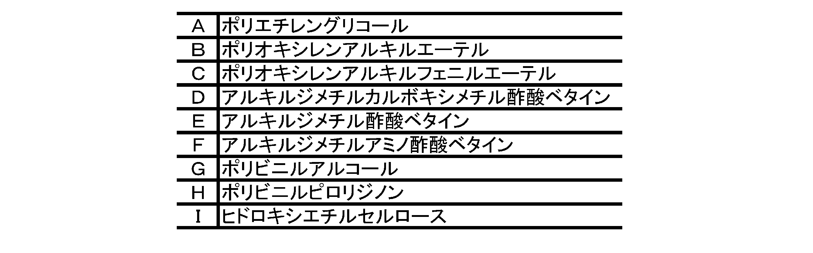
- nonionic surfactant polyoxyalkylene ether surfactants such as polyethylene glycol, polyoxyethylene alkyl ether, polyoxyethylene alkyl phenyl ether, and the like can be used.
- a betaine surfactant such as alkyldimethylacetic acid betaine, alkyldimethylcarboxymethylacetic acid betaine, and alkyldimethylaminoacetic acid betaine can be used.
- water-soluble polymer polyvinyl alcohol, polyvinyl pyrrolidinone, hydroxyethyl cellulose and the like can be used.
- the amount of the dispersant used is generally 0.5 to 30 g / L based on the volume of the liquid (electroless plating bath), although it depends on the type. In particular, the amount of the dispersant used is preferably in the range of 1 to 10 g / L with respect to the volume of the liquid (electroless plating bath) from the viewpoint of improving the adhesion of the nickel film.
- the nickel ions contained in the electroless plating bath use a water-soluble nickel salt as the nickel source.
- a water-soluble nickel salt nickel sulfate or nickel chloride can be used, but is not limited thereto.
- the concentration of nickel ions contained in the electroless plating bath is preferably 0.0001 to 0.008 mol / liter, particularly 0.0001 to 0.005 mol / liter.
- the electroless plating bath can contain a reducing agent.
- a reducing agent those similar to those used for the reduction of the noble metal ions described above can be used.
- the concentration of the reducing agent in the electroless plating bath is preferably 4 ⁇ 10 ⁇ 4 to 2.0 mol / liter, particularly 2.0 ⁇ 10 ⁇ 3 to 0.2 mol / liter.
- the electroless plating bath may further contain a complexing agent.
- a complexing agent By containing the complexing agent, an advantageous effect that the decomposition of the plating solution is suppressed is exhibited.
- the complexing agent include organic carboxylic acids or salts thereof such as citric acid, hydroxyacetic acid, tartaric acid, malic acid, lactic acid or gluconic acid, or alkali metal salts or ammonium salts thereof. These complexing agents can be used alone or in combination of two or more.
- the concentration of the complexing agent in the electroless plating bath is preferably 0.005 to 6 mol / liter, particularly 0.01 to 3 mol / liter.
- the electroless plating bath can be heated to a temperature at which nickel ions can be reduced, and the pretreated core material particles can be put into the electroless plating bath under this state.
- nickel ions are reduced, and nickel produced by the reduction forms an initial thin film layer on the surface of the core material particles.
- the initial thin film layer is preferably formed to have a thickness of 0.1 to 10 nm, particularly 0.1 to 5 nm. At this point, the protrusion has not yet been formed.
- An important point in the step A is the relationship between the amount of nickel ions contained in the electroless plating bath and the amount of core material particles to be introduced. Specifically, the total surface area for one liter of the electroless plating bath adjusted to a nickel ion concentration of 0.0001 to 0.008 mol / liter, preferably 0.0001 to 0.005 mol / liter. Is used in an amount of 1 to 15 m 2 , particularly 2 to 8 m 2 . Thereby, the initial thin film layer having the above-described thickness can be easily formed.
- the relationship between the amount of nickel ions and the amount of core material particles as described above aggregation of the core material particles on which the initial thin film layer is formed can be effectively prevented. This is particularly effective when the particle diameter of the core material particles is small, for example, when the particle diameter is 3 ⁇ m or less.
- step B nickel ions and a reducing agent are added over time to the aqueous slurry containing the core material particles having the nickel initial thin film layer obtained in step A and the dispersant used in step A. “Adding over time” is intended to exclude adding nickel ions and a reducing agent all at once, and adding nickel ions and a reducing agent continuously or intermittently over a certain period of time. Intended.
- the timing of adding the nickel ions and the reducing agent may be completely the same, or the addition of nickel ions may precede and the addition of the reducing agent may follow.
- the reverse is also possible. Further, at the end point of addition, the end of the addition of nickel ions may precede, and the end of the addition of the reducing agent may follow. The reverse is also possible.
- the same nickel source as used in the A process can be used.
- step B by reducing nickel ions, first, fine nickel core particles are generated in the liquid, and the core particles are attached to the surface of the core material particles having the nickel initial thin film layer obtained in step A. This is grown from the adhering core particles as a starting point to form a protrusion.
- aggregation of particles can be effectively prevented, and a projection having an aspect ratio of 1 or more can be easily formed.
- Patent Document 1 described in the background art section of the present specification first, a nickel film is formed on the surface of the core material particles, and a nucleus that is a starting point of the formation of the protrusion is formed (No. 1). Then, the projection is formed by growing the nucleus in the next step (second step). In this method, since the concentration of nickel ions in the first step needs to be relatively high, particle aggregation tends to occur due to this. In addition, it is difficult to form a protrusion with a high aspect ratio.
- step B it is important to maintain the aqueous slurry in a pH range in which the dispersing effect of the dispersant added in step A (this dispersant remains in step B) is exhibited. is there. Thereby, aggregation of particles can be effectively prevented.
- an acid such as various mineral acids or an alkali such as sodium hydroxide may be added to the aqueous slurry while monitoring the pH of the aqueous slurry.
- the pH adjustment range may be an appropriate value depending on the dispersant used. For example, when a nonionic surfactant is used as the dispersant, it is preferable to maintain the pH of the aqueous slurry in the range of 5 to 10.
- an amphoteric surfactant When used as the dispersant, it is preferable to maintain the pH of the aqueous slurry in the range of 5-8. Even when a water-soluble polymer is used as the dispersant, it is preferable to maintain the pH of the aqueous slurry in the range of 5 to 8.
- the amount of nickel ions and the amount of reducing agent added to the aqueous slurry are also important. As a result, it is possible to successfully form a projection having a high aspect ratio.
- nickel ions and a reducing agent are added to the aqueous slurry over time in an amount corresponding to an amount of nickel deposited per hour of 25 to 100 nm, preferably 40 to 60 nm. By adopting such an addition condition, nickel precipitates preferentially occur in the core particles rather than the initial thin film layer, and a protrusion having a high aspect ratio is easily formed.
- the aqueous slurry may be heated to a predetermined temperature so that the reduction of nickel ions by the reducing agent proceeds smoothly.
- the aqueous slurry may be stirred so that the reduced nickel adheres uniformly.
- the conductive particles can be further subjected to post-treatment as necessary.
- the post-treatment include an electroless gold plating step or an electroless palladium plating step.
- a gold plating layer or a palladium plating layer is formed on the surface of the conductive particles.
- the gold plating layer can be formed according to a conventionally known electroless plating method. For example, by adding an electroless plating solution containing tetrasodium ethylenediaminetetraacetate, disodium citrate, and potassium gold cyanide and adjusted to pH with sodium hydroxide to an aqueous suspension of conductive particles, A plating layer can be formed.
- the formation of the palladium plating layer can be performed according to a conventionally known electroless plating method. For example, reduction of water-soluble palladium compounds such as palladium chloride; hypophosphorous acid, phosphorous acid, formic acid, acetic acid, hydrazine, borohydride, amine borane compounds, or salts thereof into an aqueous suspension of conductive particles A conventional electroless palladium plating solution containing an agent; and a complexing agent, and a dispersant, a stabilizer, and a pH buffering agent are added as necessary.
- a conventional electroless palladium plating solution containing an agent; and a complexing agent, and a dispersant, a stabilizer, and a pH buffering agent are added as necessary.
- a palladium ion source such as tetraamminepalladium salt, a complexing agent and, if necessary, a dispersing agent are added to an aqueous suspension of conductive particles, and substitution is performed using a substitution reaction between palladium ions and nickel ions.
- a palladium electroplating layer may be formed by performing mold electroless plating.
- the palladium plating layer is substantially free of phosphorus or has a content reduced to 3% by weight or less from the viewpoint of excellent conductivity and electrical reliability.
- a phosphorus-free reducing agent for example, formic acid
- the same dispersants as exemplified in the above-described Step A can be used.
- the conductive particles can be subjected to a grinding process using a media mill such as a ball mill.
- a media mill such as a ball mill.
- the conductive particles of the present invention are, for example, conductive for connecting the electrodes of anisotropic conductive film (ACF), heat seal connector (HSC), and liquid crystal display panel to the circuit board of the driving LSI chip. It is suitably used as a material.
- the conductive powder of the present invention is suitably used as a conductive filler of a conductive adhesive.
- the conductive adhesive is preferably used as an anisotropic conductive adhesive that is disposed between two substrates on which a conductive base material is formed, and adheres and conducts the conductive base material by heating and pressing.
- This anisotropic conductive adhesive contains the conductive particles of the present invention and an adhesive resin.
- Any adhesive resin can be used without particular limitation as long as it is insulative and used as an adhesive resin.
- Either a thermoplastic resin or a thermosetting resin may be used, and those that exhibit adhesive performance by heating are preferred. Examples of such an adhesive resin include a thermoplastic type, a thermosetting type, and an ultraviolet curing type.
- thermosetting types that exhibit intermediate properties between thermoplastic types and thermosetting types, combined types of thermosetting types and ultraviolet curing types, and the like.
- adhesive resins can be appropriately selected according to the surface characteristics and usage pattern of the circuit board or the like to be attached.
- an adhesive resin including a thermosetting resin is preferable from the viewpoint of excellent material strength after bonding.
- the adhesive resin examples include ethylene-vinyl acetate copolymer, carboxyl-modified ethylene-vinyl acetate copolymer, ethylene-isobutyl acrylate copolymer, polyamide, polyimide, polyester, polyvinyl ether, polyvinyl butyral, and polyurethane.
- SBS block copolymer carboxyl modified SBS copolymer, SIS copolymer, SEBS copolymer, maleic acid modified SEBS copolymer, polybutadiene rubber, chloroprene rubber, carboxyl modified chloroprene rubber, styrene-butadiene rubber, isobutylene- Isoprene copolymer, acrylonitrile-butadiene rubber (hereinafter referred to as NBR), carboxyl-modified NBR, amine-modified NBR, epoxy resin, epoxy ester resin, acrylic resin, phenol resin, Those prepared as main agent one obtained by one or more combinations selected from and a silicone resin.
- NBR acrylonitrile-butadiene rubber
- thermoplastic resin styrene-butadiene rubber, SEBS, and the like are preferable because they have excellent reworkability.
- thermosetting resin an epoxy resin is preferable. Of these, epoxy resins are most preferred because of their advantages of high adhesive strength, excellent heat resistance and electrical insulation, low melt viscosity, and connection at low pressure.
- epoxy resin a generally used epoxy resin can be used as long as it is a polyvalent epoxy resin having two or more epoxy groups in one molecule.
- novolak resins such as phenol novolak and cresol novolak
- polyhydric phenols such as bisphenol A, bisphenol F, bisphenol AD, resorcin, and bishydroxydiphenyl ether
- ethylene glycol, neopentyl glycol, glycerin and trimethylolpropane.
- polychlorohydric alcohols such as polypropylene glycol, polyamino compounds such as ethylenediamine, triethylenetetramine and aniline, polycarboxylic compounds such as adipic acid, phthalic acid and isophthalic acid with epichlorohydrin or 2-methylepichlorohydrin.
- a glycidyl type epoxy resin is exemplified.
- aliphatic and alicyclic epoxy resins such as dicyclopentadiene epoxide and butadiene dimer epoxide are listed. These can be used alone or in admixture of two or more.
- the various adhesive resins described above use high-purity products in which impurity ions (such as Na and Cl) and hydrolyzable chlorine are reduced.
- the amount of the conductive particles of the present invention used in the anisotropic conductive adhesive is usually 0.1 to 30 parts by weight, preferably 0.5 to 25 parts by weight, more preferably 1 to 100 parts by weight of the adhesive resin component. ⁇ 20 parts by weight.
- the amount of the conductive particles used is within this range, an increase in connection resistance and melt viscosity is suppressed, connection reliability is improved, and connection anisotropy can be sufficiently secured.
- the anisotropic conductive adhesive can be blended with known additives in the technical field, and the blending amount is also known in the technical field. Can be within range.
- additives include, for example, tackifiers, reactive auxiliaries, epoxy resin curing agents, metal oxides, photoinitiators, sensitizers, curing agents, vulcanizing agents, deterioration inhibitors, heat resistant additives, heat Examples thereof include a conductivity improver, a softener, a colorant, various coupling agents, or a metal deactivator.
- tackifier examples include rosin, rosin derivatives, terpene resins, terpene phenol resins, petroleum resins, coumarone-indene resins, styrene resins, isoprene resins, alkylphenol resins, xylene resins and the like.
- the reactive assistant that is, the crosslinking agent include polyols, isocyanates, melamine resins, urea resins, utropines, amines, acid anhydrides and peroxides.
- curing agent if it has two or more active hydrogen in 1 molecule, it can use without a restriction
- polyamino compounds such as diethylenetriamine, triethylenetetramine, metaphenylenediamine, dicyandiamide, and polyamideamine
- organic acid anhydrides such as phthalic anhydride, methyl nadic anhydride, hexahydrophthalic anhydride, and pyromellitic anhydride.
- novolak resins such as phenol novolac and cresol novolak. These can be used alone or in admixture of two or more. Moreover, you may use a latent hardening
- latent curing agents examples include imidazole series, hydrazide series, boron trifluoride-amine complexes, sulfonium salts, amine imides, polyamine salts, dicyandiamide, and the like and modified products thereof. These can be used alone or as a mixture of two or more.
- the anisotropic conductive adhesive is usually prepared by using a manufacturing apparatus widely used among those skilled in the art, and blends the conductive particles and adhesive resin of the present invention and, if necessary, curing agents and various additives,
- the adhesive resin is a thermosetting resin
- it is mixed in an organic solvent.
- the adhesive resin is a thermoplastic resin
- the temperature is higher than the softening point of the adhesive resin, and preferably about 50 to 130 ° C. More preferably, it is produced by melt-kneading at about 60 to 110 ° C.
- the anisotropic conductive adhesive thus obtained may be applied or applied in the form of a film.
- Step A Spherical styrene-silica composite resin (trade name: Soliostar, manufactured by Nippon Shokubai Co., Ltd.) having a particle size shown in Table 1 and a true specific gravity of 1.1 was used as the core material particles.
- 40 g of the solution was added to 400 mL of an aqueous conditioner solution (“Cleaner Conditioner 231” manufactured by Rohm and Haas Electronic Materials) with stirring.
- the concentration of the conditioner aqueous solution was 40 ml / L.
- the core material particles were surface-modified and dispersed by stirring for 30 minutes while applying ultrasonic waves at a liquid temperature of 60 ° C.
- the aqueous solution was filtered, and the core particles washed once with repulp water were made into 200 mL of slurry. 200 ml of stannous chloride aqueous solution was added to this slurry. The concentration of this aqueous solution was 5 ⁇ 10 ⁇ 3 mol / L. The mixture was stirred at room temperature for 5 minutes to carry out a sensitization treatment for adsorbing tin ions on the surface of the core material particles. Subsequently, the aqueous solution was filtered and washed once with repulp water. The core particles were then made into 400 ml slurry and maintained at 60 ° C.
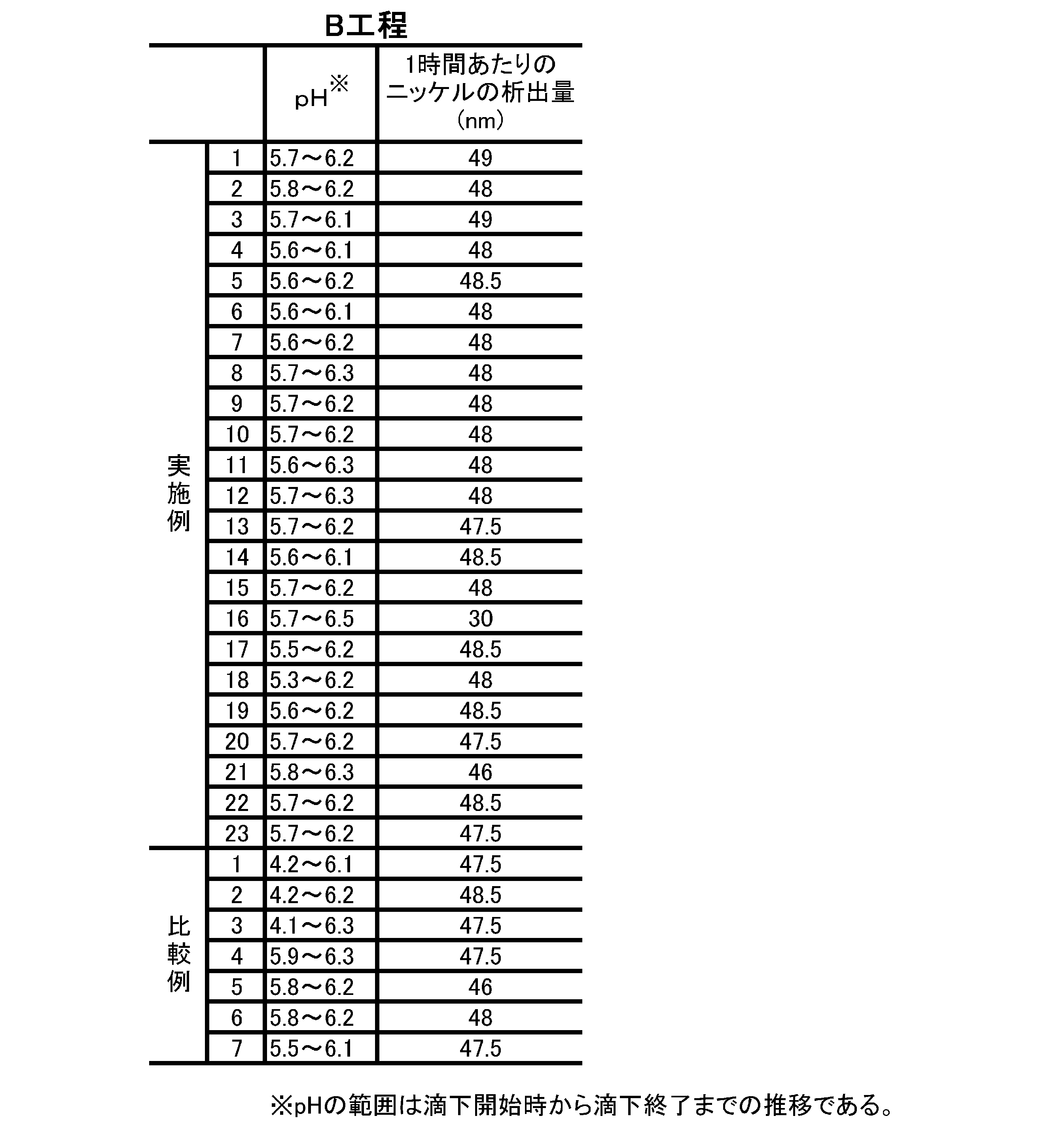
- Step B Using a 224 g / L nickel sulfate aqueous solution and a mixed aqueous solution containing 210 g / L sodium hypophosphite and 80 g / L sodium hydroxide, 300 mL each, and using these in step A, the core material obtained
- the particle slurry was continuously fractionated and added by a metering pump, and the electroless plating B process was started. The addition rate was 2.5 mL / min. Specific conditions of this step are shown in Table 3. After all the liquid was added, stirring was continued for 5 minutes while maintaining the temperature at 70 ° C. Next, the liquid was filtered, and the filtrate was washed three times, and then dried with a vacuum dryer at 100 ° C. to obtain conductive particles having a nickel-phosphorus alloy film. A scanning electron microscope (SEM) image of the conductive particles obtained in Example 3 is shown in FIG. As is clear from the figure, the nickel coating and the protrusions on the conductive particles are continuous.
- SEM
- Examples 5 to 23 Conductive particles were obtained in the same manner as in Example 1 except that Step A and Step B were performed under the conditions shown in Tables 1 and 3.
- the addition amount of nickel sulfate aqueous solution and the mixed aqueous solution containing sodium hypophosphite and sodium hydroxide was 230 mL, respectively.
- the addition amount of nickel sulfate aqueous solution and the mixed aqueous solution containing sodium hypophosphite and sodium hydroxide was 390 mL, respectively.
- the addition amount and dropping rate of the aqueous nickel sulfate solution of Examples 21 to 23 and the mixed aqueous solution containing sodium hypophosphite and sodium hydroxide were 150, 225, 600 mL, 1.3, 1.9, and 5.0 mL, respectively. / Min. In this way, conductive particles having a nickel-phosphorus alloy film were obtained.
- Example 24 An electroless gold plating solution consisting of 10 g / L EDTA-4Na, 10 g / L citric acid-2Na, and 2.9 g / L potassium gold cyanide (2.0 g / L as Au) was prepared. 2 g of this gold plating solution was heated to 79 ° C., and 10 g of conductive particles obtained in Example 2 were added while stirring the solution. Thus, electroless plating treatment was performed on the surface of the particles. The processing time was 20 minutes. After completion of the treatment, the liquid was filtered and the filtrate was repulped three times. Subsequently, it dried with the 110 degreeC vacuum dryer. In this way, a gold plating coating treatment was performed on the nickel-phosphorus alloy film.
- Examples 25 to 27 10 g / L EDTA-2Na, 10 g / L 2Na citrate and 20 g / L tetraamminepalladium hydrochloride (Pd (NH 3 ) 4 Cl 2 ) solution (2 g / L as palladium), carboxymethylcellulose (molecular weight 250,000, ether An electroless palladium plating solution having a degree of conversion of 0.9) 100 ppm was prepared. The palladium plating solution 0.65 liter (Example 25), 1.3 liter (Example 16), 2.6 liter (Example 27) was heated to 70 ° C. 10 g of the obtained conductive particles were added.
- a substitutional electroless plating treatment was performed on the surface of the particles.
- the processing time was 60 minutes.
- the liquid was filtered and the filtrate was repulped three times. Subsequently, it dried with the 110 degreeC vacuum dryer. In this way, a palladium plating coating treatment was performed on the nickel-phosphorus alloy film.
- the palladium film contained no phosphorus.
- Comparative Example 8 The conductive particles produced in Comparative Example 2 were subjected to the same gold plating coating treatment as in Example 24.
- A [(r + t) 3 ⁇ r 3 ] d 1 / r 3 d 2 (1)
- A W / (100-W) (2)
- r is the radius ( ⁇ m) of the core particles
- t is the thickness of the nickel coating
- d 1 is the specific gravity of the nickel coating
- d 2 is the specific gravity of the core particles
- W is the nickel content (% by weight).
- Gold film / palladium film thickness The conductive particles were immersed in aqua regia to dissolve the gold or palladium film and the nickel film, and the film components were analyzed by ICP or chemical analysis. And the thickness of the gold
- coat was computed from the following (3) and (4).
- B [(r + t + u) 3 ⁇ (r + t) 3 ] d 3 / (r + t) 3 d 4 (3)
- B X (100 ⁇ X) (4)
- u is the thickness of the gold or palladium film
- d 3 is the specific gravity of the gold or palladium film
- d 4 is the specific gravity of the Ni product
- X is the content (% by weight) of gold or palladium.
- the specific gravity d 4 of the Ni product is calculated using a calculation formula. The specific gravity was calculated using the following formula (5).
- d 4 100 / [(W / d 1 ) + (100 ⁇ W) / d 2 ] (5)
- d 1 is the specific gravity of the nickel coating
- d 2 is the specific gravity of the core particles
- W is the nickel content (% by weight).
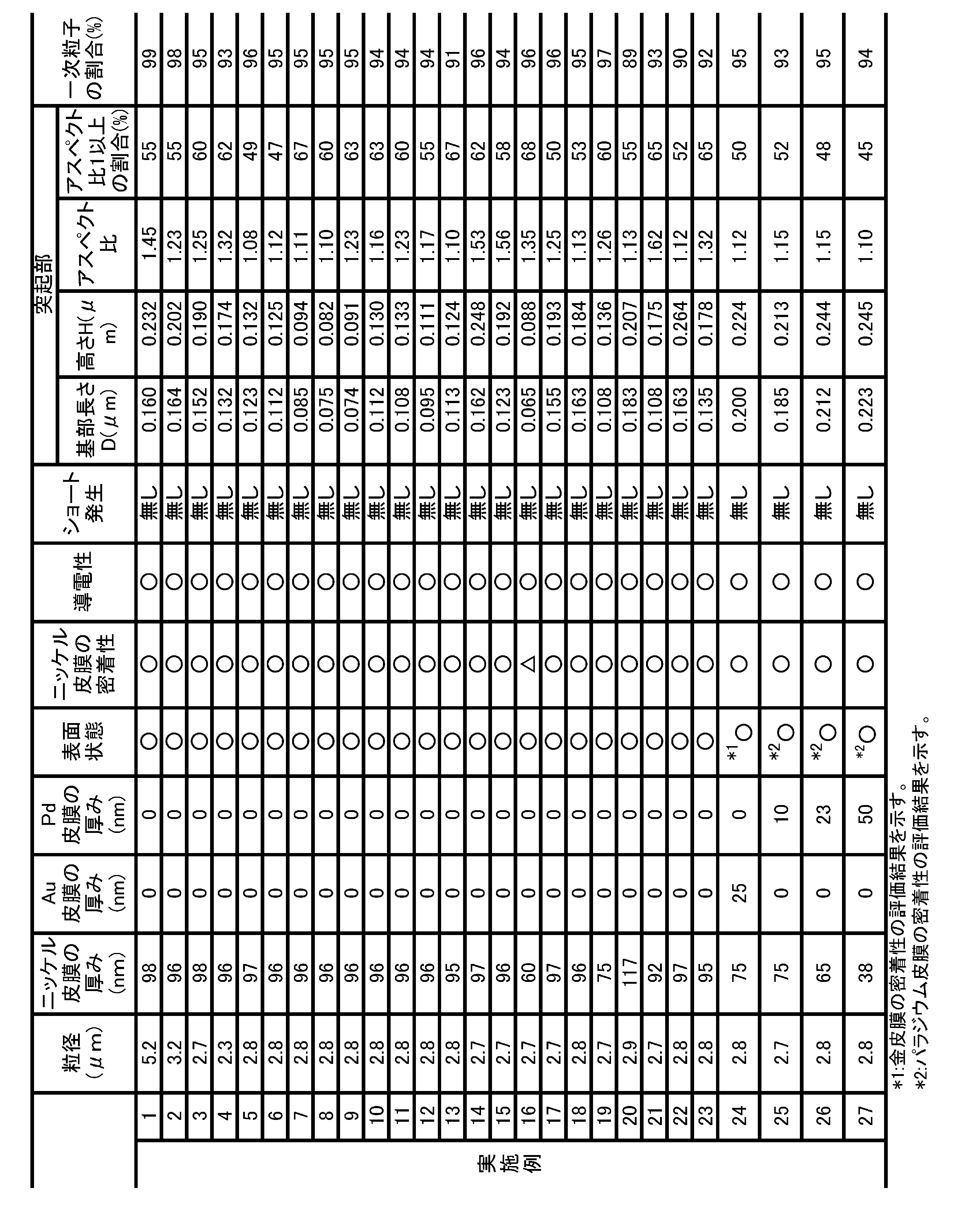
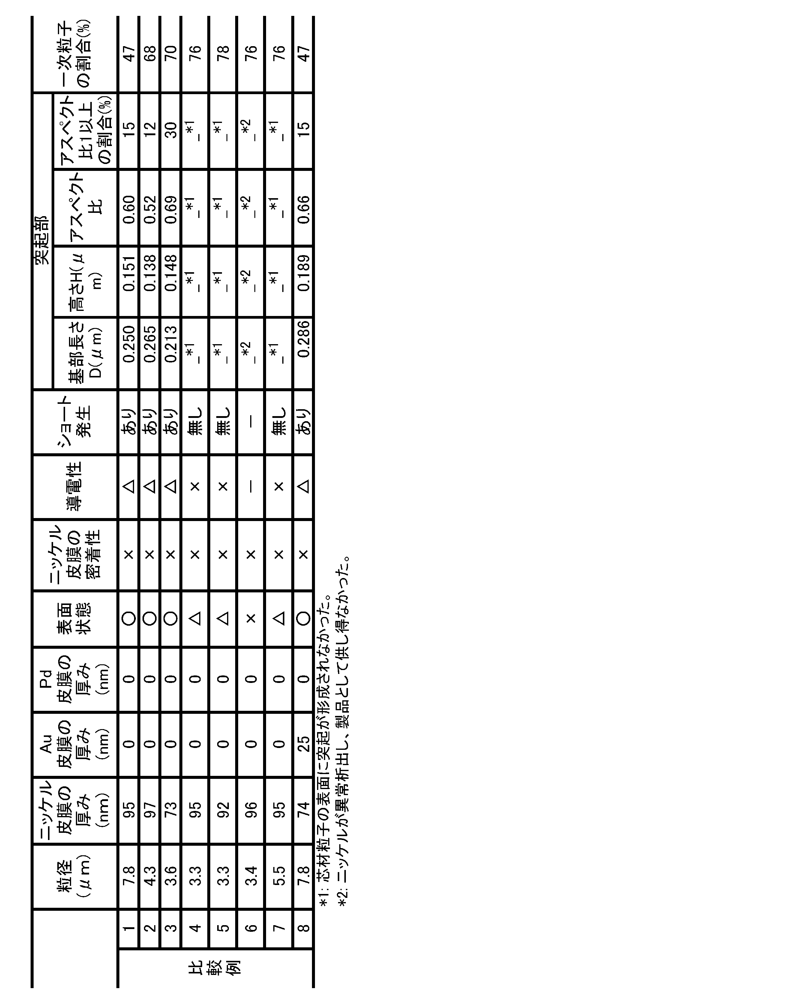
- the conductive powder obtained in each example has an aspect ratio of protrusions compared to the conductive powder obtained in the comparative example. It can be seen that the ratio of primary particles is high. Moreover, it turns out that the electroconductive powder obtained by each Example has high electroconductivity and the adhesiveness of a nickel membrane
- the conductive powder of the present invention has good dispersibility and conductivity even though the particle size of the conductive particles constituting the conductive powder is smaller than the conventional one. Moreover, according to the manufacturing method of this invention, such electroconductive powder can be manufactured easily.
Landscapes
- Chemical & Material Sciences (AREA)
- Engineering & Computer Science (AREA)
- Mechanical Engineering (AREA)
- Metallurgy (AREA)
- General Chemical & Material Sciences (AREA)
- Chemical Kinetics & Catalysis (AREA)
- Organic Chemistry (AREA)
- Materials Engineering (AREA)
- Dispersion Chemistry (AREA)
- Physics & Mathematics (AREA)
- Spectroscopy & Molecular Physics (AREA)
- Manufacturing & Machinery (AREA)
- Microelectronics & Electronic Packaging (AREA)
- Conductive Materials (AREA)
- Non-Insulated Conductors (AREA)
- Powder Metallurgy (AREA)
Abstract
Description
変動係数(%)=(標準偏差/平均粒径)×100 (1)
この変動係数が大きいことは分布に幅があることを示し、一方、変動係数が小さいことは粒度分布がシャープであることを示す。本発明では、芯材粒子として、この変動係数が30%以下、特に20%以下、とりわけ10%以下のものを使用することが好ましい。この理由は、本発明の導電性粒子を異方導電フィルム中の導電粒子として用いた場合に、接続に有効な寄与割合が高くなるという利点があるからである。
式(2)で示されるF及びSは、微小圧縮試験機MCTM-500((株)島津製作所製)で測定したときの、それぞれ該微球体の10%圧縮変形における荷重値(kgf)及び圧縮変位(mm)であり、Rは該微球体の半径(mm)である。
(1)A工程
表1に示す粒径を有し、真比重が1.1の球状スチレン-シリカ複合樹脂〔(株)日本触媒製、商品名ソリオスター〕を芯材粒子として用いた。その40gを、400mLのコンディショナー水溶液(ローム・アンド・ハース電子材料製の「クリーナーコンディショナー231」)に攪拌しながら投入した。コンディショナー水溶液の濃度は40ml/Lであった。引き続き、液温60℃で超音波を与えながら30分間攪拌して芯材粒子の表面改質及び分散処理を行った。水溶液をろ過し、一回リパルプ水洗した芯材粒子を200mLのスラリーにした。このスラリーへ塩化第一錫水溶液200mlを投入した。この水溶液の濃度は5×10-3mol/Lであった。常温で5分攪拌し、錫イオンを芯材粒子の表面に吸着させる感受性化処理を行った。引き続き水溶液をろ過し、1回リパルプ水洗した。次いで芯材粒子を400mlのスラリーにし、60℃に維持した。超音波を併用してスラリーを攪拌しながら、0.11mol/Lの塩化パラジウム水溶液2mLを添加した。そのままの攪拌状態を5分間維持させ、芯材粒子の表面にパラジウムイオンを捕捉させる活性化処理を行った。
224g/L硫酸ニッケル水溶液と、210g/Lの次亜リン酸ナトリウム及び80g/Lの水酸化ナトリウムを含む混合水溶液とをそれぞれ300mL用い、これらをA工程で得られた芯材粒子のスラリーに、定量ポンプによって連続的に分別添加し、無電解めっきB工程を開始した。添加速度はいずれも2.5mL/分とした。本工程の具体的な条件を表3に示す。液を全量添加した後、70℃の温度を保持しながら5分攪拌を継続した。次いで液をろ過し、ろ過物を3回洗浄した後、100℃の真空乾燥機で乾燥してニッケル-リン合金皮膜を有する導電性粒子を得た。実施例3において得られた導電性粒子の走査型電子顕微鏡(SEM)像を図1に示した。同図から明らかなように、導電性粒子におけるニッケル皮膜と突起部とは連続体になっている。
表1及び表3に示す条件でA工程及びB工程を行う以外は実施例1と同様にして導電性粒子を得た。ただし、実施例19のB工程においては、硫酸ニッケル水溶液と、次亜リン酸ナトリウム及び水酸化ナトリウムを含む混合水溶液の添加量をそれぞれ230mLとした。また実施例20のB工程においては、硫酸ニッケル水溶液と、次亜リン酸ナトリウム及び水酸化ナトリウムを含む混合水溶液の添加量をそれぞれ390mLとした。また実施例21ないし23の硫酸ニッケル水溶液と、次亜リン酸ナトリウム及び水酸化ナトリウムを含む混合水溶液の添加量及び滴下速度はそれぞれ150、225、600mL、1.3、1.9、5.0mL/分とした。このようにして、ニッケル-リン合金皮膜を有する導電性粒子を得た。
10g/LのEDTA-4Na、10g/Lのクエン酸―2Na及び2.9g/Lのシアン化金カリウム(Auとして2.0g/L)からなる無電解金めっき液を調製した。この金めっき液2リットルを79℃に加熱し、これを攪拌しながら、実施例2で得られた導電性粒子10gを添加した。これによって粒子の表面に無電解めっき処理を行った。処理時間は20分とした。処理の完了後、液をろ過し、ろ過物を3回リパルプした。次いで110℃の真空乾燥機で乾燥した。このようにして、ニッケル-リン合金皮膜上に金めっき被覆処理を施した。
10g/LのEDTA-2Na、10g/Lのクエン酸2Na及び20g/Lのテトラアンミンパラジウム塩酸塩(Pd(NH3)4Cl2)溶液(パラジウムとして2g/L)、カルボキシメチルセルロース(分子量250000、エーテル化度0.9)100ppmからなる無電解パラジウムめっき液を調製した。このパラジウムめっき液0.65リットル(実施例25)、1.3リットル(実施例16)、2.6リットル(実施例27)を70℃に加熱し、これを攪拌しながら、実施例2で得られた導電性粒子10gを添加した。これによって粒子の表面に置換型の無電解めっき処理を行った。処理時間は60分とした。処理の完了後、液をろ過し、ろ過物を3回リパルプした。次いで110℃の真空乾燥機で乾燥した。このようにして、ニッケル-リン合金皮膜上にパラジウムめっき被覆処理を施した。パラジウム皮膜中にリンは含まれていなかった。
表1及び表3に示す条件でA工程及びB工程を行う以外は実施例1と同様にして、ニッケル―リン合金皮膜を有する導電性粒子を得た。ただし、比較例3のB工程においては、硫酸ニッケル水溶液と、次亜リン酸ナトリウム及び水酸化ナトリウムを含む混合水溶液の添加量をそれぞれ230mLとした。また比較例5ないし6の硫酸ニッケル水溶液と、次亜リン酸ナトリウム及び水酸化ナトリウムを含む混合水溶液の添加量及び滴下速度はそれぞれ38、1200mL、0.3、10.0mL/分とした。比較例1において得られた導電性粒子のSEM像を図2に示した。
比較例2で製造した導電性粒子に、実施例24と同様の金めっき被覆処理を施した。
実施例及び比較例で得られた導電性粒子の粒径、ニッケル皮膜の厚み、金皮膜の厚み、パラジウム皮膜の厚み、表面状態、ニッケル皮膜の密着性及び導電性をそれぞれ測定・評価した。また、更に金めっきを施したものは、金皮膜の密着性、パラジウムめっきを施したものは、パラジウム皮膜の密着性を評価した。各物性評価は次の方法によって行った。また、突起部のアスペクト比、アスペクト比が1以上である突起部の割合、及び導電性粉体における一次粒子が占める割合、導電性粒子の粒径をそれぞれ上述の方法で測定した。それらの結果を表4及び表5に示す。
導電性粒子を王水に浸漬してニッケル皮膜を溶解し、皮膜成分をICP又は化学分析し、以下の式(1)、(2)からニッケル皮膜の厚みを算出した。
A=[(r+t)3―r3]d1/r3d2 (1)
A=W/(100-W) (2)
式中、rは芯材粒子の半径(μm)、tはニッケル皮膜の厚み、d1はニッケル皮膜の比重、d2は芯材粒子の比重、Wはニッケル含有率(重量%)である。
導電性粒子を王水に浸漬して、金又はパラジウム皮膜とニッケル皮膜とを溶解し、皮膜成分をICP分析又は化学分析した。そして、以下の(3)及び(4)から金又はパラジウム皮膜の厚みを算出した。
B=[(r+t+u)3-(r+t)3]d3/(r+t)3d4 (3)
B=X(100-X) (4)
式中、uは金又はパラジウム皮膜の厚み、d3は金又はパラジウム皮膜の比重、d4はNi品の比重、Xは金又はパラジウムの含有率(重量%)である。ここで、Ni品の比重d4は計算式を使用して算出する。比重は以下の(5)の計算式を用いて算出した。
d4=100/[(W/d1)+(100-W)/d2] (5)
式中、d1はニッケル皮膜の比重、d2は芯材粒子の比重、Wはニッケル含有率(重量%)である。
SEMを用い、導電性粒子を30000倍に拡大して10視野を観察し、導電性粒子1個が有する突起部の個数の平均値を算出した。10~100個を○、10以下を△とした。また、ニッケルが異常析出した場合を×とした。異常析出とは、例えばニッケルが芯材粒子の表面に析出せず、液中に単独析出する場合等を言う。
100mLのビーカーに導電性粒子2g及び直径1mmのジルコニアビーズ90gを入れ、更にトルエンを10mL入れた。攪拌装置で10分攪拌した後、ジルコニアビーズとスラリーを分離し乾燥させた。乾燥後の導電性粒子をSEMを用いて2000倍に拡大して10視野を観察し、攪拌によって生じた剥離片の個数の平均値を算出した。剥離片の個数10個未満を○とし、10~30個を△、30個超を×とした。
エポキシ樹脂100部、硬化剤150部、トルエン70部を混合し、絶縁性接着剤を調製した。これに導電性粒子15部を配合してペーストを得た。バーコーターを用い、このペーストをシリコーン処理ポリエステルフィルム上に塗布し乾燥させた。得られた塗工フィルムを用い、全面をアルミニウムで蒸着したガラスと50μmピッチに銅パターンを形成したポリイミドフィルム基板との間の接続を行った。そして電極間の導通抵抗を測定することで、導電性粒子の導電性を評価した。評価は抵抗値2Ω以下を○とし、2~5Ωを△、5Ω以上を×とした。また、ショート発生の有無も表に併記した。

Claims (7)
- 芯材粒子の表面に、ニッケル又はニッケル合金皮膜が形成された導電性粒子からなる導電性粉体であって、
前記導電性粒子は、前記皮膜の表面から突出し、かつ該皮膜と連続体になっている、アスペクト比が1以上の突起部を多数有し、アスペクト比が1以上の前記突起部の割合が、全突起部の数に対して40%以上であり、前記導電性粉体においては、前記導電性粒子のうち、一次粒子が占める重量が、導電性粉体の重量に対して85重量%以上であることを特徴とする導電性粉体。 - 前記芯材粒子の平均粒径が1~3μmである請求項1記載の導電性粉体。
- 前記突起部を含む前記皮膜の表面を金又はパラジウムで被覆した請求項1又は2記載の導電性粉体。
- 請求項1ないし3のいずれかに記載の導電性粉体と絶縁性樹脂とを含む導電性材料。
- 分散剤及びニッケルイオンを含む無電解めっき浴と、表面に貴金属が担持された芯材粒子とを混合して、該芯材粒子の表面にニッケル初期薄膜層を形成するに際し、ニッケルイオンの濃度が0.0001~0.008モル/リットルに調整された該無電解めっき浴1リットルに対して、表面積の総和が1~15m2となるような量の該芯材粒子を用いるA工程と、
A工程において得られた、ニッケル初期薄膜層を有する前記芯材粒子、及び前記分散剤を含む水性スラリーを、該分散剤の分散効果が発現するpH範囲に維持しつつ、該水性スラリーに、1時間当たりのニッケルの析出量が25~100nmとなる量に相当する量のニッケルイオン及び還元剤を経時的に添加して、該水性スラリー中にニッケルの核粒子を生成させるとともに、生成した核粒子を前記芯材粒子に付着させて、付着した核粒子を起点として該核粒子を成長させ、アスペクト比が1以上の突起部を形成するB工程とを具備することを特徴とする導電性粒子の製造方法。 - ニッケル初期薄膜層の厚みが0.1~10nmとなるようにA工程を行う請求項5記載の製造方法。
- 前記分散剤として、非イオン界面活性剤、両性イオン界面活性剤又は水溶性高分子を用いる請求項5又は6記載の製造方法。
Priority Applications (1)
| Application Number | Priority Date | Filing Date | Title |
|---|---|---|---|
| CN200980140898XA CN102187405B (zh) | 2008-10-14 | 2009-10-13 | 导电性粉体和包含该导电性粉体的导电性材料以及导电性颗粒的制造方法 |
Applications Claiming Priority (4)
| Application Number | Priority Date | Filing Date | Title |
|---|---|---|---|
| JP2008-264725 | 2008-10-14 | ||
| JP2008264725 | 2008-10-14 | ||
| JP2009220045A JP4746116B2 (ja) | 2008-10-14 | 2009-09-25 | 導電性粉体及びそれを含む導電性材料並びに導電性粒子の製造方法 |
| JP2009-220045 | 2009-09-25 |
Publications (1)
| Publication Number | Publication Date |
|---|---|
| WO2010044388A1 true WO2010044388A1 (ja) | 2010-04-22 |
Family
ID=42106551
Family Applications (1)
| Application Number | Title | Priority Date | Filing Date |
|---|---|---|---|
| PCT/JP2009/067707 Ceased WO2010044388A1 (ja) | 2008-10-14 | 2009-10-13 | 導電性粉体及びそれを含む導電性材料並びに導電性粒子の製造方法 |
Country Status (5)
| Country | Link |
|---|---|
| JP (1) | JP4746116B2 (ja) |
| KR (1) | KR101594639B1 (ja) |
| CN (1) | CN102187405B (ja) |
| TW (1) | TWI479508B (ja) |
| WO (1) | WO2010044388A1 (ja) |
Cited By (5)
| Publication number | Priority date | Publication date | Assignee | Title |
|---|---|---|---|---|
| JP2012178270A (ja) * | 2011-02-25 | 2012-09-13 | Hitachi Chem Co Ltd | 導電粒子及びその製造方法、接着剤組成物、回路接続材料、接続構造体、並びに回路部材の接続方法 |
| JP2013008474A (ja) * | 2011-06-22 | 2013-01-10 | Nippon Shokubai Co Ltd | 導電性微粒子の製造方法 |
| JP2015109271A (ja) * | 2013-10-23 | 2015-06-11 | 積水化学工業株式会社 | 導電性粒子、導電材料及び接続構造体 |
| JP2015149277A (ja) * | 2014-01-10 | 2015-08-20 | 積水化学工業株式会社 | 導電性粒子、導電性粒子の製造方法、導電材料及び接続構造体 |
| KR101815336B1 (ko) | 2010-09-30 | 2018-01-04 | 세키스이가가쿠 고교가부시키가이샤 | 도전성 입자, 이방성 도전 재료 및 접속 구조체 |
Families Citing this family (22)
| Publication number | Priority date | Publication date | Assignee | Title |
|---|---|---|---|---|
| JP5512306B2 (ja) * | 2010-01-29 | 2014-06-04 | 日本化学工業株式会社 | 導電性粒子の製造方法 |
| JP5476221B2 (ja) * | 2010-06-18 | 2014-04-23 | 積水化学工業株式会社 | 導電性粒子、異方性導電材料及び接続構造体 |
| JP5184612B2 (ja) | 2010-11-22 | 2013-04-17 | 日本化学工業株式会社 | 導電性粉体、それを含む導電性材料及びその製造方法 |
| KR101097862B1 (ko) * | 2011-03-04 | 2011-12-23 | 덕산하이메탈(주) | 도전입자 및 그 제조방법 |
| JP5707247B2 (ja) * | 2011-06-22 | 2015-04-22 | 日本化学工業株式会社 | 導電性粒子の製造方法 |
| KR101191970B1 (ko) * | 2011-12-09 | 2012-10-17 | 한화케미칼 주식회사 | 인 도핑된 니켈 나노 입자 및 이의 제조방법 |
| JP5952553B2 (ja) * | 2011-12-14 | 2016-07-13 | 株式会社日本触媒 | 導電性微粒子及びこれを含む異方性導電材料 |
| JP5951977B2 (ja) * | 2011-12-14 | 2016-07-13 | 株式会社日本触媒 | 導電性微粒子 |
| KR101375298B1 (ko) * | 2011-12-20 | 2014-03-19 | 제일모직주식회사 | 전도성 미립자 및 이를 포함하는 이방 전도성 필름 |
| WO2013108740A1 (ja) * | 2012-01-19 | 2013-07-25 | 積水化学工業株式会社 | 導電性粒子、導電材料及び接続構造体 |
| JP5973257B2 (ja) * | 2012-07-03 | 2016-08-23 | 日本化学工業株式会社 | 導電性粒子及びそれを含む導電性材料 |
| KR101443347B1 (ko) * | 2013-05-14 | 2014-10-02 | 덕산하이메탈(주) | 도전입자 및 그 제조방법 |
| JP6352103B2 (ja) * | 2013-08-12 | 2018-07-04 | 積水化学工業株式会社 | 導電性粒子、導電材料及び接続構造体 |
| JP6523860B2 (ja) * | 2014-08-07 | 2019-06-05 | 積水化学工業株式会社 | 導電性粒子、導電材料及び接続構造体 |
| JP6641118B2 (ja) * | 2014-08-18 | 2020-02-05 | 積水化学工業株式会社 | 導電性粒子、導電材料及び接続構造体 |
| JP6263228B2 (ja) * | 2016-06-09 | 2018-01-17 | 日本化学工業株式会社 | 導電性粒子及びそれを含む導電性材料 |
| TWI783938B (zh) * | 2016-06-22 | 2022-11-21 | 日商積水化學工業股份有限公司 | 連接結構體、含金屬原子之粒子及連接用組成物 |
| CN110157363B (zh) * | 2019-06-11 | 2021-04-06 | 莱芜职业技术学院 | 一种电磁屏蔽导电胶用导电粉末的制备方法 |
| FR3100822B1 (fr) * | 2019-09-12 | 2021-10-01 | Lifco Ind | Billes de soudure composites metallisees en surface et calibrees pour l'assemblage de cartes electroniques |
| KR20230011946A (ko) * | 2020-05-20 | 2023-01-25 | 니폰 가가쿠 고교 가부시키가이샤 | 도전성 입자, 그것을 사용한 도전성 재료 및 접속 구조체 |
| KR102908614B1 (ko) * | 2020-08-24 | 2026-01-06 | 니폰 가가쿠 고교 가부시키가이샤 | 피복 입자 및 그 제조 방법 |
| FR3119172A1 (fr) * | 2021-01-28 | 2022-07-29 | Swissto12 Sa | Composition stable pour dépôt catalytique d’argent |
Citations (3)
| Publication number | Priority date | Publication date | Assignee | Title |
|---|---|---|---|---|
| JP2000243132A (ja) * | 1999-02-22 | 2000-09-08 | Nippon Chem Ind Co Ltd | 導電性無電解めっき粉体とその製造方法並びに該めっき粉体からなる導電性材料 |
| JP2004296322A (ja) * | 2003-03-27 | 2004-10-21 | Sekisui Chem Co Ltd | 導電性微粒子及び液晶表示素子 |
| JP2006228474A (ja) * | 2005-02-15 | 2006-08-31 | Sekisui Chem Co Ltd | 導電性微粒子及び異方性導電材料 |
Family Cites Families (3)
| Publication number | Priority date | Publication date | Assignee | Title |
|---|---|---|---|---|
| US5378407A (en) * | 1992-06-05 | 1995-01-03 | Raychem Corporation | Conductive polymer composition |
| TW277152B (ja) * | 1994-05-10 | 1996-06-01 | Hitachi Chemical Co Ltd | |
| US6013713A (en) * | 1997-11-06 | 2000-01-11 | International Business Machines Corporation | Electrode modification using an unzippable polymer paste |
-
2009
- 2009-09-25 JP JP2009220045A patent/JP4746116B2/ja active Active
- 2009-10-07 TW TW098133952A patent/TWI479508B/zh active
- 2009-10-13 CN CN200980140898XA patent/CN102187405B/zh active Active
- 2009-10-13 KR KR1020117008427A patent/KR101594639B1/ko active Active
- 2009-10-13 WO PCT/JP2009/067707 patent/WO2010044388A1/ja not_active Ceased
Patent Citations (3)
| Publication number | Priority date | Publication date | Assignee | Title |
|---|---|---|---|---|
| JP2000243132A (ja) * | 1999-02-22 | 2000-09-08 | Nippon Chem Ind Co Ltd | 導電性無電解めっき粉体とその製造方法並びに該めっき粉体からなる導電性材料 |
| JP2004296322A (ja) * | 2003-03-27 | 2004-10-21 | Sekisui Chem Co Ltd | 導電性微粒子及び液晶表示素子 |
| JP2006228474A (ja) * | 2005-02-15 | 2006-08-31 | Sekisui Chem Co Ltd | 導電性微粒子及び異方性導電材料 |
Cited By (5)
| Publication number | Priority date | Publication date | Assignee | Title |
|---|---|---|---|---|
| KR101815336B1 (ko) | 2010-09-30 | 2018-01-04 | 세키스이가가쿠 고교가부시키가이샤 | 도전성 입자, 이방성 도전 재료 및 접속 구조체 |
| JP2012178270A (ja) * | 2011-02-25 | 2012-09-13 | Hitachi Chem Co Ltd | 導電粒子及びその製造方法、接着剤組成物、回路接続材料、接続構造体、並びに回路部材の接続方法 |
| JP2013008474A (ja) * | 2011-06-22 | 2013-01-10 | Nippon Shokubai Co Ltd | 導電性微粒子の製造方法 |
| JP2015109271A (ja) * | 2013-10-23 | 2015-06-11 | 積水化学工業株式会社 | 導電性粒子、導電材料及び接続構造体 |
| JP2015149277A (ja) * | 2014-01-10 | 2015-08-20 | 積水化学工業株式会社 | 導電性粒子、導電性粒子の製造方法、導電材料及び接続構造体 |
Also Published As
| Publication number | Publication date |
|---|---|
| JP4746116B2 (ja) | 2011-08-10 |
| TW201021054A (en) | 2010-06-01 |
| TWI479508B (zh) | 2015-04-01 |
| KR101594639B1 (ko) | 2016-02-16 |
| JP2010118334A (ja) | 2010-05-27 |
| CN102187405A (zh) | 2011-09-14 |
| KR20110069811A (ko) | 2011-06-23 |
| CN102187405B (zh) | 2013-01-02 |
Similar Documents
| Publication | Publication Date | Title |
|---|---|---|
| JP4746116B2 (ja) | 導電性粉体及びそれを含む導電性材料並びに導電性粒子の製造方法 | |
| JP5184612B2 (ja) | 導電性粉体、それを含む導電性材料及びその製造方法 | |
| JP5512306B2 (ja) | 導電性粒子の製造方法 | |
| CN103531271B (zh) | 导电性粒子、导电性材料及导电性粒子的制造方法 | |
| JP5941328B2 (ja) | 導電性粒子及びそれを含む導電性材料 | |
| JP5695768B2 (ja) | 導電性粉体及びそれを含む導電性材料 | |
| JP6263228B2 (ja) | 導電性粒子及びそれを含む導電性材料 | |
| WO2026070639A1 (ja) | 導電性粒子の製造方法 |
Legal Events
| Date | Code | Title | Description |
|---|---|---|---|
| WWE | Wipo information: entry into national phase |
Ref document number: 200980140898.X Country of ref document: CN |
|
| 121 | Ep: the epo has been informed by wipo that ep was designated in this application |
Ref document number: 09820566 Country of ref document: EP Kind code of ref document: A1 |
|
| ENP | Entry into the national phase |
Ref document number: 20117008427 Country of ref document: KR Kind code of ref document: A |
|
| NENP | Non-entry into the national phase |
Ref country code: DE |
|
| 122 | Ep: pct application non-entry in european phase |
Ref document number: 09820566 Country of ref document: EP Kind code of ref document: A1 |