WO2010038554A1 - 光学部品の製造方法並びにレンズ、レンズユニット及びカメラモジュール - Google Patents
光学部品の製造方法並びにレンズ、レンズユニット及びカメラモジュール Download PDFInfo
- Publication number
- WO2010038554A1 WO2010038554A1 PCT/JP2009/064389 JP2009064389W WO2010038554A1 WO 2010038554 A1 WO2010038554 A1 WO 2010038554A1 JP 2009064389 W JP2009064389 W JP 2009064389W WO 2010038554 A1 WO2010038554 A1 WO 2010038554A1
- Authority
- WO
- WIPO (PCT)
- Prior art keywords
- lens
- array
- optical component
- information
- manufacturing
- Prior art date
- Legal status (The legal status is an assumption and is not a legal conclusion. Google has not performed a legal analysis and makes no representation as to the accuracy of the status listed.)
- Ceased
Links
Images



Classifications
-
- G—PHYSICS
- G02—OPTICS
- G02B—OPTICAL ELEMENTS, SYSTEMS OR APPARATUS
- G02B13/00—Optical objectives specially designed for the purposes specified below
- G02B13/001—Miniaturised objectives for electronic devices, e.g. portable telephones, webcams, PDAs, small digital cameras
- G02B13/0085—Miniaturised objectives for electronic devices, e.g. portable telephones, webcams, PDAs, small digital cameras employing wafer level optics
-
- G—PHYSICS
- G02—OPTICS
- G02B—OPTICAL ELEMENTS, SYSTEMS OR APPARATUS
- G02B13/00—Optical objectives specially designed for the purposes specified below
- G02B13/001—Miniaturised objectives for electronic devices, e.g. portable telephones, webcams, PDAs, small digital cameras
- G02B13/0015—Miniaturised objectives for electronic devices, e.g. portable telephones, webcams, PDAs, small digital cameras characterised by the lens design
- G02B13/002—Miniaturised objectives for electronic devices, e.g. portable telephones, webcams, PDAs, small digital cameras characterised by the lens design having at least one aspherical surface
- G02B13/003—Miniaturised objectives for electronic devices, e.g. portable telephones, webcams, PDAs, small digital cameras characterised by the lens design having at least one aspherical surface having two lenses
-
- G—PHYSICS
- G02—OPTICS
- G02B—OPTICAL ELEMENTS, SYSTEMS OR APPARATUS
- G02B3/00—Simple or compound lenses
- G02B3/0006—Arrays
- G02B3/0037—Arrays characterized by the distribution or form of lenses
- G02B3/0056—Arrays characterized by the distribution or form of lenses arranged along two different directions in a plane, e.g. honeycomb arrangement of lenses
-
- G—PHYSICS
- G02—OPTICS
- G02B—OPTICAL ELEMENTS, SYSTEMS OR APPARATUS
- G02B3/00—Simple or compound lenses
- G02B3/0006—Arrays
- G02B3/0037—Arrays characterized by the distribution or form of lenses
- G02B3/0062—Stacked lens arrays, i.e. refractive surfaces arranged in at least two planes, without structurally separate optical elements in-between
- G02B3/0068—Stacked lens arrays, i.e. refractive surfaces arranged in at least two planes, without structurally separate optical elements in-between arranged in a single integral body or plate, e.g. laminates or hybrid structures with other optical elements
-
- G—PHYSICS
- G02—OPTICS
- G02B—OPTICAL ELEMENTS, SYSTEMS OR APPARATUS
- G02B7/00—Mountings, adjusting means, or light-tight connections, for optical elements
- G02B7/02—Mountings, adjusting means, or light-tight connections, for optical elements for lenses
- G02B7/022—Mountings, adjusting means, or light-tight connections, for optical elements for lenses lens and mount having complementary engagement means, e.g. screw/thread
Definitions
- the present invention relates to a method of manufacturing an optical component and a lens, a lens unit, and a camera module manufactured by the method of manufacturing an optical component.
- a manufacturing method of a camera module that is divided and cut out as one camera module is known (see Patent Document 1).
- a method of manufacturing an optical component capable of printing various information including information on individual optical components on each optical component relatively easily and It aims at providing the lens manufactured using this, a lens unit, and a camera module.
- an optical component manufacturing method includes: (a) an optical component in which a stacked optical component array including a lens array in which a plurality of lenses are arranged is divided into individual optical components and taken out. (B) a lens array molding step for molding a lens array from an optical material, (c) an array stacking step for obtaining an optical component array by attaching the lens array to another stacked component, and (d And (e) a pattern including information relating to each lens of the lens array between the lens array forming process and the array dividing process. And a pattern printing process for printing on the optical surface.
- a process including a pattern including information on each lens of the lens array is printed on the non-optical surface of each lens between the lens array molding process and the array dividing process.
- the pattern is printed on the non-optical surface of the surface of each lens.
- information about individual optical components can be printed collectively on the surface of the lens array, so that various types of information including information about individual optical components can be accurately specified for each optical component. Can be displayed.
- the optical component array has (a1) a first lens array as a lens array, and (a2) a plurality of lenses corresponding to each lens of the first lens array.
- a second lens array as another laminated component, and (b) in the pattern printing step, each lens on the non-optical surface of the surface of at least one of the first and second lens arrays.
- a pattern including information relating to each lens unit corresponding to is printed. In this case, information about each lens unit formed by dividing the optical component array including the first and second lens arrays is relatively transferred to the non-optical surface of the surface of any lens constituting each lens unit. Easy to print.
- an optical component array corresponds to (a1) a lens array, and (a2) each lens of the lens array, and each camera module cooperates with each lens.
- information on each camera module corresponding to each lens in each lens of the lens array in the pattern printing step. Is printed on the non-optical surface of the surface of each lens.
- information regarding each camera module formed by dividing the optical component array including the lens array and the image sensor wafer is relatively easily printed on the non-optical surface of the surface of the lens constituting each camera module. be able to.
- the optical component array is configured by further stacking filter members for cutting incident light in a predetermined wavelength region.
- the filter member can remove unnecessary components from the light passing through the optical component, for example.
- the pattern including each information is printed by applying a resin to the non-optical surface of the surface of each lens and curing the resin.
- pattern printing can be performed relatively easily by applying and curing the resin.
- a pattern including each information is printed by laser processing a non-optical surface of the surface of each lens.
- pattern printing can be performed accurately and reliably by the laser processing.
- information printed on the non-optical surface of the surface of each lens includes information obtained in at least one of the lens array molding process and the array stacking process. It is characterized by. In this case, information unique to each lens that is determined during the manufacturing process can be included in the printed pattern.
- information printed on the non-optical surface of each lens surface includes information on an arrangement position of each lens in the lens array.
- information about the position and orientation of each lens in the lens array can be included in the printed pattern as information unique to each lens.
- the lens according to the present invention has a pattern including information on each lens as its own manufacturing information by being formed by any one of the optical component manufacturing methods described above. It is characterized by. In this case, manufacturing information is displayed on each lens formed by being divided.
- the lens unit according to the present invention is formed by any one of the optical component manufacturing methods described above, and thus has a pattern including information on each lens as its own manufacturing information. It is characterized by that. In this case, manufacturing information is displayed on each of the lens units that are individually divided.
- the camera module according to the present invention has a pattern including information on each lens as its own manufacturing information by being formed by any one of the optical component manufacturing methods described above. It is characterized by that. In this case, manufacturing information is displayed on each of the camera modules formed separately.
- (A), (b) is a perspective view which shows the manufacturing process of the camera module containing the lens unit which concerns on 1st Embodiment. It is a top view for demonstrating the array division
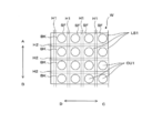
- FIGS. 1A and 1B are perspective views illustrating an outline of a manufacturing process of a camera module which is an example of an optical component according to the first embodiment.
- FIGS. 2 and 3 are manufacturing processes of the camera module. It is the top view and side sectional view which show typically the optical component array formed by.
- the optical component array W includes first and second lens arrays W1 and W2 and an image sensor wafer IW which is another laminated component. . That is, the optical component array W is obtained by laminating these laminated components in the order of the image sensor wafer IW, the first lens array W1, and the second lens array W2, and bonding them together with an ultraviolet curable resin or the like.
- the first lens array W1 is composed of a large number of lenses LS1 arranged in a matrix.
- each lens LS1 includes a lens body OU1 having a curved lens surface used as an optical system, and a non-optical surface having a non-optical surface that is a peripheral part of the lens body OU1 and is not used as an optical system.
- the system part BK is comprised.
- the second lens array W2 includes a plurality of lenses LS2 having a matrix arrangement corresponding to the plurality of lenses LS1 constituting the first lens array W1.
- the image sensor wafer IW has a structure in which a large number of image sensor chips CI are arranged in a matrix so as to correspond to the large number of lenses LS1 and LS2, respectively.
- Each image sensor chip CI is composed of, for example, a photoelectric conversion element or the like, and receives light after passing through each lens body OU1, OU2 and converts it into an electrical signal, thereby cooperating with each lens LS1, LS2.
- the camera module 10 that functions as a camera is configured.
- the camera module 10 is cut out and individually divided by cutting the optical component array W with, for example, a dicing blade DS as shown in FIG. More specifically, as shown in FIGS. 2 and 3, each of the arrays W1, W2, and IW constituting the optical component array W has H1 and H2 that are cut between portions to be the camera module 10, Corresponding to the arrangement of a large number of lenses LS1, LS2 and image sensor chip CI arranged in a matrix, they are provided in a grid. For example, when the optical component array W is cut using the dicing blade DS as shown in FIG. 1B, the width of the cutting margin H1 (H2) is determined corresponding to the width of the dicing blade DS.
- the lens unit LU and the image sensor chip CI having the rectangular side surfaces with the cutting line CT that is the both ends of the cutting margin H1 (H2) as a boundary portion and having the side surfaces of the lenses LS1 and LS2.
- the camera module 10 having a three-layer structure with the optical element portion LS3 having the above is cut out individually.
- each camera module 10 taken out by dividing the optical component array W as described above is the surface of the lens LS1, and is formed by the surfaces of the lens body OU1 and the non-optical system portion BK.
- manufacturing information of each optical component is printed on the surface SF of the non-optical system part BK, which is a non-optical surface (not shown).
- Such printing is performed in a method of manufacturing an optical component in which a single optical component array W is divided and a plurality of optical components are manufactured in a lump, and before the division, the surface SF of the non-optical system portion BK is formed. This is realized by a pattern printing process in which manufacturing information regarding individual optical components is collectively written on such a non-optical surface.
- FIG. 4 is a block diagram conceptually illustrating a manufacturing apparatus 100 for the camera module 10 which is an example of an optical component
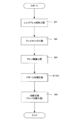
- FIG. 5 is a flowchart for explaining a manufacturing method for the camera module 10 using the manufacturing apparatus 100. It is.
- the manufacturing apparatus 100 includes a molding machine 110 that molds the first and second lens arrays W1 and W2 from an optical material such as a transparent resin, and first and second lenses formed by the molding machine 110.
- the lens array W2 and the image sensor wafer IW are laminated and pasted (see FIGS. 1A and 1B) to form a laminated portion 130 for forming the optical component array W, and an optical formed by the laminated portion 130.
- a cutting machine 140 that divides the component array W to form individual camera modules 10.
- the manufacturing apparatus 100 is a printing machine that performs a printing process on the first lens array W1 among the arrays W1, W2, and IW accumulated in the stock unit 120 in addition to the above-described essential parts for manufacturing. 150.
- the printing machine 150 is a printing unit that performs printing on the surface SF of the non-optical part BK of the first lens array W1 shown in FIG. 2 and the like. For example, a resin is applied to the surface SF by inkjet or the like, and the resin is cured. By doing so, a pattern for displaying various information including information on each lens of the camera module 10 is printed.
- the printing machine 150 receives information from the print head 160 for performing the pattern printing operation, the stage 170 on which a subject to be printed by the print head 160 is placed, and each part of the manufacturing apparatus 100 to determine the pattern to be printed.
- a data processing unit 180 that collects and processes the information.
- the data processing unit 180 includes a ROM 180a and a RAM 180b, and stores various information such as character data to be printed.
- the ROM 180a can be rewritten, but basically does not need to be rewritten in the operation of the manufacturing apparatus 100, such as the version and product name of each optical component, the manufacturer, the manufacturing location, and the optical component. It has a data area for storing various information such as design information such as orientation in the optical component array W.
- the RAM 180a has a data area for holding various information such as information that changes at any time with the operation of the manufacturing apparatus 100, for example, manufacturing date, lot number, and forming conditions regarding parts and the like. Information that changes from time to time is transmitted from the molding machine 110, the stock unit 120, and the like to the data processing unit 180.
- the data processing unit 180 determines the contents of the pattern to be printed based on the information accumulated in the ROM 180a and the RAM 180b.
- the manufacturing apparatus 100 executes an operation for forming the camera module 10 according to the flowchart of FIG. That is, first, a lens array molding process is performed in which the first and second lens arrays W1 and W2 are molded by the molding machine 110 (step S1). Next, the process proceeds to an array stock process in which the first and second lens arrays W1 and W2 and the image sensor wafer IW are accumulated in the stock unit 120 (step S2). At this time, it is determined which of the accumulated arrays W1, W2, and IW and which combination is stacked. That is, the combination of the laminated components that constitute the optical component array W is determined.
- the printing machine 150 proceeds to a pattern printing process in which a pattern is printed on the first lens array W1 based on the information stored in the ROM 180a and the RAM 180b (step S3). That is, the specific first lens array W ⁇ b> 1 is taken out from the stock unit 120 and conveyed onto the stage 170 of the printing machine 150. Using the print head 160, the first lens array W1 conveyed on the stage 170 is printed on the non-optical system portion BK positioned around each lens body OU1 shown in FIG. The printing method is performed all at once on the surface of the first lens array W1 by, for example, ink jetting. The printing pattern corresponds to each one of the camera modules 10.
- the camera module 10 is in a state equivalent to that printed in units of one by one.
- the printed first lens array W1 is returned to the stock unit 120 again.
- the arrays W1, W2, and IW whose combinations are determined are sent from the stock unit 120 to the stack unit 130.
- an array stacking process for forming the optical component array W by stacking the arrays W1, W2, and IW is performed (step S4).
- a cutting process is performed by the cutting machine 140 to cut the optical component array W formed with the stacked unit 130 to form a large number of camera modules 10 (step S5). That is, when the cutting machine 140 includes, for example, the dicing blade DS shown in FIG. 1B, the optical component array W is divided and the camera modules 10 are individually cut out one by one.
- FIG. 6 is a flowchart for explaining the processing performed by the data processing unit 180 as the preceding stage of the printing process in step S3 of FIG.
- the data processing unit 180 first passes through a component data processing step for determining data to be printed (step S31), creates data to be printed (step S32), and issues a printing operation command. (Step S33).
- the determination process of the data to be printed performed in step S31 is performed based on the information accumulated in the ROM 180a and the RAM 180b as described above. More specifically, first, as shown in FIG.
- IF1 is transmitted from the molding machine 110 to the RAM 180b of the data processing unit 180.
- the transmission is based on the premise that all necessary data is prepared, and is performed after the arrays W1 and W2 are formed by the array forming process in step S1 of FIG.
- the first lens array W1 stored in the stock unit 120 or the information IF2 related to the second lens array W2 and the image sensor wafer IW combined therewith is stored in the data processing unit 180.
- the RAM 180b In step S31 of FIG.
- the data processing unit 280 temporarily stores the information IF1 and IF2 in the RAM 180b, determines whether the information is correct or not based on the collected information, and the data in the ROM 180a and the RAM 180b. Of these, the contents to be displayed on each camera module 10 are determined. As a method for determining whether the information is correct or incorrect, for example, information of identification numbers given to the trays that carry the first lens arrays W1 in the information IF1 and the information IF2 is obtained and compared. Each first lens array W1 is identified by this correctness determination.
- FIG. 7 is a front view showing an example of the manufactured optical component.
- the data processing unit 180 has information about the first lens array W1 and the like after being molded. Therefore, as shown in FIG. 7, for example, information unique to each lens LS ⁇ b> 1, that is, each camera module 10 can be included as a pattern PM ⁇ b> 1 formed on the surface SF of the non-optical system portion BK of each camera module 10.
- the pattern PM1 indicates “manufacturing date / serial number / position information before cutting” by numerical values. In this way, information such as in which position and orientation of the lens LS1 in the first lens array W1 in FIG. 1 and the like can be included for each camera module 10.
- the orientation of the camera module 10 can be determined from the positions and arrangement of the printed characters of the patterns PM1 and PM2, and from this information, for example, the position and direction when the camera module 10 is incorporated into each device can be determined.
- step S3 the pattern to be printed on each camera module 10 is simultaneously applied to the surface of the first lens array W1 before the camera modules 10 are individually divided. Is going to. For this reason, for example, it is possible to easily print information as compared with the case where the camera modules 10 are handled one by one and manufacturing information is printed. Further, since the contents to be printed are determined based on the information about the first lens array W1 and the like after being molded, information specific to each camera module 10 is also included.
- FIG. 8 is a block diagram for explaining an example of an optical component manufacturing apparatus according to the second embodiment
- FIG. 9 is for explaining a camera module manufacturing method using the manufacturing apparatus according to the present embodiment. It is a flowchart of.
- the manufacturing apparatus 200 according to the present embodiment is a modification of the manufacturing apparatus 100 shown in FIG. 4, and the operations and functions of the same reference numerals as those of the manufacturing apparatus 100 of FIG. The detailed explanation is omitted.
- the manufacturing apparatus 200 includes a molding machine 110, a stock unit 120, a stacking unit 130, a cutting machine 140, and a printing machine 250 that performs a printing process on the surface of the optical component array W.
- the printing machine 250 is a printing unit that performs printing on the non-optical part BK of the first lens array W1 that is the surface of the optical component array W shown in FIG.
- the printing machine 250 prints various information patterns including information about each lens of the camera module 10 on the optical component array W formed in the stacking unit 130.
- the printing machine 250 includes a print head 160 and a stage 170, and further includes a data processing unit 280 that processes each piece of information in order to determine a pattern to be printed.
- the data processing unit 280 includes Among the parts of the manufacturing apparatus 200, information is collected not only from the molding machine 110 and the stock part 120 but also from the lamination part 130.
- the data processing unit 280 includes a ROM 180a and a RAM 180b.
- the ROM 180a has a data area in which fixed information is stored.
- the RAM 180b is information that changes sequentially for each part. A data area for holding information transmitted from the machine 110, the stock unit 120, and the stacking unit 130.
- the operation of the manufacturing apparatus 200 for forming the camera module 10 will be described with reference to the flowchart of FIG.
- the first and second lens arrays W1 and W2 are formed by the molding machine 110 (step S1).
- the second lens arrays W1 and W2 and the image sensor wafer IW are accumulated (step S2).
- the optical component array W is formed from the arrays W1, W2, and IW in the stacking unit 130 (step S4).
- the information IF1 to IF3 relating to the first and second lens arrays W1 and W2, the image sensor wafer IW, and the optical component array W formed by stacking these in the respective steps S1, S2 and S4 are data.
- the data is transmitted to the RAM 180b of the processing unit 280.
- the data processing unit 280 determines whether the information is correct by comparing information about the first lens array W1 obtained from the information IF1 to IF3, for example, and also determines whether each of the camera modules 10 out of the data in the ROM 180a and the RAM 180b. The contents to be displayed are determined.
- the optical component array W formed in step S ⁇ b> 4 moves from the stacking unit 130 onto the stage 170 of the printing machine 250.
- Step S103 a pattern regarding the determined printing content is printed on the surface SF of the non-optical system portion BK of each camera module 10 shown in FIG.
- Step S103 the optical component array W laminated by the laminating unit 130 and subjected to the printing pattern by the printing machine 250 is cut by the cutting machine 140 to form a large number of camera modules 10 (step S5).
- a pattern including information regarding each lens is printed on the optical component array W in which the arrays W1, W2, and IW are stacked. Also in this case, since printing is performed simultaneously on the surface of the optical component array W, information unique to each camera module 10 can be easily printed as in the case of the first embodiment. Can be applied to each of the camera modules 10 one by one. In particular, in the present embodiment, information related to the combination of the arrays W1, W2, and IW, that is, information related to the optical component array W can also be displayed on each camera module 10.
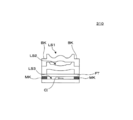
- FIG. 10 is a side sectional view for explaining a camera module which is an optical component according to the third embodiment.
- the camera module 310 according to this embodiment is a modification of the camera module 10 shown in the first embodiment and the like, and a predetermined wavelength region is incident between the lens LS2 and the optical element unit LS3 having the image sensor chip CI. It has a structure having a filter member FT for cutting light. More specifically, an example of the filter member FT will be described.
- the filter member FT is an infrared absorption filter that absorbs infrared light, and removes unnecessary infrared light from the light beams that have passed through the lens LS1 and the lens LS2.
- the camera module 310 has a structure including the filter member FT for removing infrared light in addition to the optical element unit LS3 including the lens LS1, the lens LS2, and the image sensor chip CI. It has an advanced camera function. Note that a mask MK is formed around the image sensor chip CI in order to prevent the filter member FT from contacting the image sensor chip CI.
- the mask MK and the filter member FT are previously formed on the image sensor wafer IW. What is necessary is just to form the film which should become.
- the mask MK and the filter member FT are cut out together as components in the camera module 310. Therefore, in this case, operations in each manufacturing process such as pattern printing can be performed in the same manner as in the first embodiment.
- the laminated structure has three layers.
- the present invention is not limited to this, and the present invention can be applied to an optical component having more layers and an optical component having a two-layer structure.
- the camera module is manufactured as an optical component.
- the manufactured optical component may be other than the camera module.
- FIG. 1A and the like if each of the above embodiments is used for a two-layered optical component array composed of a first lens array W1 and a second lens array W2, a lens unit having a two-layer structure Can be manufactured.
- a pattern including the information is printed. That is, each lens unit has its own manufacturing information on the non-optical surface.
- a lens having its own manufacturing information on a non-optical surface can be manufactured using each of the above embodiments.
- the pattern printing method on the surface of each array W1, W is not limited to the ink jet method as long as the entire surface is printed, and various methods can be applied. It is also possible to form a pattern by laser processing the surface SF of the system part BK.
Landscapes
- Physics & Mathematics (AREA)
- General Physics & Mathematics (AREA)
- Optics & Photonics (AREA)
- Lens Barrels (AREA)
- Studio Devices (AREA)
- Transforming Light Signals Into Electric Signals (AREA)
- Solid State Image Pick-Up Elements (AREA)
Abstract
Description
図1(A)、(B)は、第1実施形態に係る光学部品の一例であるカメラモジュールの製造工程の概要について示す斜視図であり、図2及び図3は、当該カメラモジュールの製造過程で形成される光学部品アレイを模式的に示す平面図及び側断面図である。
図8は、第2実施形態に係る光学部品の製造装置の一例を説明するためのブロック図であり、図9は、本実施形態に係る製造装置を用いたカメラモジュールの製造方法を説明するためのフローチャートである。なお、本実施形態に係る製造装置200は、図4に示す製造装置100の変形例であり、図4の製造装置100と同符号のものについては、動作や機能等は同様であるので、詳細な説明を省略する。
図10は、第3実施形態に係る光学部品であるカメラモジュールを説明するための側断面図である。本実施形態に係るカメラモジュール310は、第1実施形態等に示すカメラモジュール10の変形例であり、レンズLS2とイメージセンサチップCIを有する光学素子部LS3との間に、所定の波長領域の入射光をカットするためのフィルタ部材FTを有する構造となっている。フィルタ部材FTの一例についてより具体的に説明すると、フィルタ部材FTは、赤外光を吸収する赤外吸収フィルタであり、レンズLS1及びレンズLS2を通過した光線から不要な赤外光を除去することによってイメージセンサチップCIにおける像の劣化を防止している。以上のように、カメラモジュール310は、レンズLS1、レンズLS2及びイメージセンサチップCIを有する光学素子部LS3に加えて、赤外光を除去するためのフィルタ部材FTを有する構造であることによって、より高度なカメラ機能を有するものとなる。なお、フィルタ部材FTがイメージセンサチップCIに接触することを回避するために、イメージセンサチップCIの周囲にはマスクMKが形成されている。
W1、W2…レンズアレイ
IW…イメージセンサウエハ
LS1、LS2…レンズ
CI…イメージセンサチップ
10、310…カメラモジュール
FT…フィルタ部材
100、200…製造装置
110…成形機
120…ストック部
130…積層部
140…切断機
150、250…印刷機
180、280…データ処理部
Claims (11)
- 複数のレンズが配置されるレンズアレイを含む積層型の光学部品アレイを個々の光学部品に分割して取り出す光学部品の製造方法であって、
光学材料から前記レンズアレイを成形するレンズアレイ成形工程と、
前記レンズアレイを他の積層部品に貼り付けて前記光学部品アレイを得るアレイ積層工程と、
前記光学部品アレイを個々の要素に分割するアレイ分割工程と、
前記レンズアレイ成形工程から前記アレイ分割工程までの間に、前記レンズアレイの各レンズに関する情報を含むパターンを当該各レンズの表面の非光学面に印刷するパターン印刷工程と
を有することを特徴とする光学部品の製造方法。 - 前記光学部品アレイは、前記レンズアレイとしての第1のレンズアレイと、前記第1のレンズアレイの各レンズに対応する複数のレンズを有する前記他の積層部品としての第2のレンズアレイとを有し、
前記パターン印刷工程において、前記第1及び第2のレンズアレイのうち少なくとも一方の各レンズの表面の非光学面に、当該各レンズに対応する各レンズユニットに関する情報を含むパターンを印刷することを特徴とする、請求項1記載の光学部品の製造方法。 - 前記光学部品アレイは、前記レンズアレイと、前記レンズアレイの各レンズに対応するとともに当該各レンズと協働してそれぞれカメラモジュールを構成する複数のイメージセンサチップを配置した前記他の積層部品としてのイメージセンサウエハとを有し、
前記パターン印刷工程において、前記レンズアレイの各レンズに、当該各レンズに対応する各カメラモジュールに関する情報を含むパターンを当該各レンズの表面の非光学面に印刷することを特徴とする、請求項1及び請求項2のいずれか一項記載の光学部品の製造方法。 - 前記光学部品アレイは、所定の波長領域の入射光をカットするためのフィルタ部材をさらに積層して構成されることを特徴とする、請求項1から請求項3までのいずれか一項記載の光学部品の製造方法。
- 前記パターン印刷工程において、各情報を含むパターンは、前記各レンズの表面の非光学面に樹脂を塗布し、当該樹脂を硬化させることにより印刷されることを特徴とする、請求項1から請求項4までのいずれか一項記載の光学部品の製造方法。
- 前記パターン印刷工程において、各情報を含むパターンは、前記各レンズの表面の非光学面をレーザ加工することで印刷されることを特徴とする、請求項1から請求項4までのいずれか一項記載の光学部品の製造方法。
- 前記パターン印刷工程において、各レンズの表面の非光学面に印刷される情報は、前記レンズアレイ成形工程及び前記アレイ積層工程のうち少なくとも1つの工程において得られる情報を含むことを特徴とする、請求項1から請求項6までのいずれか一項記載の光学部品の製造方法。
- 前記パターン印刷工程において、各レンズの表面の非光学面に印刷される情報は、当該各レンズのレンズアレイ内での配置位置についての情報を含むことを特徴とする、請求項1から請求項7までのいずれか一項記載の光学部品の製造方法。
- 上記請求項1から請求項8までのいずれか一項記載の光学部品の製造方法によって形成されることにより、前記各レンズに関する情報を含むパターンを自己の製造情報として有することを特徴とするレンズ。
- 上記請求項1から請求項8までのいずれか一項記載の光学部品の製造方法によって形成されることにより、前記各レンズに関する情報を含むパターンを自己の製造情報として有することを特徴とするレンズユニット。
- 上記請求項1から請求項8までのいずれか一項記載の光学部品の製造方法によって形成されることにより、前記各レンズに関する情報を含むパターンを自己の製造情報として有することを特徴とするカメラモジュール。
Priority Applications (2)
| Application Number | Priority Date | Filing Date | Title |
|---|---|---|---|
| US13/121,283 US8456742B2 (en) | 2008-09-30 | 2009-08-17 | Optical component manufacturing method, and lens, lens unit and camera module |
| JP2010531789A JP5429176B2 (ja) | 2008-09-30 | 2009-08-17 | 光学部品の製造方法並びに光学部品、レンズユニット及びカメラモジュール |
Applications Claiming Priority (2)
| Application Number | Priority Date | Filing Date | Title |
|---|---|---|---|
| JP2008254448 | 2008-09-30 | ||
| JP2008-254448 | 2008-09-30 |
Publications (1)
| Publication Number | Publication Date |
|---|---|
| WO2010038554A1 true WO2010038554A1 (ja) | 2010-04-08 |
Family
ID=42073329
Family Applications (1)
| Application Number | Title | Priority Date | Filing Date |
|---|---|---|---|
| PCT/JP2009/064389 Ceased WO2010038554A1 (ja) | 2008-09-30 | 2009-08-17 | 光学部品の製造方法並びにレンズ、レンズユニット及びカメラモジュール |
Country Status (3)
| Country | Link |
|---|---|
| US (1) | US8456742B2 (ja) |
| JP (1) | JP5429176B2 (ja) |
| WO (1) | WO2010038554A1 (ja) |
Cited By (2)
| Publication number | Priority date | Publication date | Assignee | Title |
|---|---|---|---|---|
| JP2012226202A (ja) * | 2011-04-21 | 2012-11-15 | Konica Minolta Advanced Layers Inc | レンズユニットの製造方法 |
| CN107718611A (zh) * | 2017-09-27 | 2018-02-23 | 重庆大学 | 一种基于3d打印和负压模具成型的仿生复眼制备方法 |
Families Citing this family (5)
| Publication number | Priority date | Publication date | Assignee | Title |
|---|---|---|---|---|
| JP5572355B2 (ja) * | 2009-09-30 | 2014-08-13 | 富士フイルム株式会社 | レンズアレイ及びレンズアレイ積層体 |
| US20140003777A1 (en) * | 2012-07-02 | 2014-01-02 | Commscope, Inc. Of North Carolina | Light focusing structures for fiber optic communications systems and methods of fabricating the same using semiconductor processing and micro-machining techniques |
| USD763939S1 (en) * | 2014-04-02 | 2016-08-16 | Cephalogics, LLC | Optical sensor array liner with optical sensor array pad |
| USD763938S1 (en) * | 2014-04-02 | 2016-08-16 | Cephalogics, LLC | Optical sensor array |
| USD765754S1 (en) * | 2014-06-26 | 2016-09-06 | Emcore Corporation | Wafer level focus lens assembly |
Citations (4)
| Publication number | Priority date | Publication date | Assignee | Title |
|---|---|---|---|---|
| JP2002046046A (ja) * | 2000-08-04 | 2002-02-12 | Seiko Epson Corp | 被加工物の加工方法及び被加工物の前処理装置 |
| JP2002290842A (ja) * | 2001-03-23 | 2002-10-04 | Sanyo Electric Co Ltd | 固体撮像素子の製造方法 |
| JP2003084243A (ja) * | 2001-09-17 | 2003-03-19 | Menicon Co Ltd | 眼用レンズのマーキング方法 |
| JP2004256381A (ja) * | 2003-02-28 | 2004-09-16 | Konica Minolta Holdings Inc | 光学素子成形方法、光学素子成形用の成形型及び光学素子 |
Family Cites Families (5)
| Publication number | Priority date | Publication date | Assignee | Title |
|---|---|---|---|---|
| JP4454292B2 (ja) * | 2002-11-26 | 2010-04-21 | 日立マクセル株式会社 | プラスチックレンズの製造方法及びその製造装置 |
| JP2004229167A (ja) | 2003-01-27 | 2004-08-12 | Sanyo Electric Co Ltd | カメラモジュールの製造方法 |
| JP2004226872A (ja) * | 2003-01-27 | 2004-08-12 | Sanyo Electric Co Ltd | カメラモジュール及びその製造方法 |
| KR20080047002A (ko) * | 2006-11-24 | 2008-05-28 | 엘지이노텍 주식회사 | 카메라모듈의 렌즈 어셈블리 및 그 제작 방법 |
| ITTO20070620A1 (it) * | 2007-08-31 | 2009-03-01 | Giancarlo Capaccio | Sistema e metodo per presentare dati visuali rilevati a distanza in immagini multi-spettrali, di fusione, ed a tre dimensioni spaziali. |
-
2009
- 2009-08-17 WO PCT/JP2009/064389 patent/WO2010038554A1/ja not_active Ceased
- 2009-08-17 US US13/121,283 patent/US8456742B2/en not_active Expired - Fee Related
- 2009-08-17 JP JP2010531789A patent/JP5429176B2/ja not_active Expired - Fee Related
Patent Citations (4)
| Publication number | Priority date | Publication date | Assignee | Title |
|---|---|---|---|---|
| JP2002046046A (ja) * | 2000-08-04 | 2002-02-12 | Seiko Epson Corp | 被加工物の加工方法及び被加工物の前処理装置 |
| JP2002290842A (ja) * | 2001-03-23 | 2002-10-04 | Sanyo Electric Co Ltd | 固体撮像素子の製造方法 |
| JP2003084243A (ja) * | 2001-09-17 | 2003-03-19 | Menicon Co Ltd | 眼用レンズのマーキング方法 |
| JP2004256381A (ja) * | 2003-02-28 | 2004-09-16 | Konica Minolta Holdings Inc | 光学素子成形方法、光学素子成形用の成形型及び光学素子 |
Cited By (2)
| Publication number | Priority date | Publication date | Assignee | Title |
|---|---|---|---|---|
| JP2012226202A (ja) * | 2011-04-21 | 2012-11-15 | Konica Minolta Advanced Layers Inc | レンズユニットの製造方法 |
| CN107718611A (zh) * | 2017-09-27 | 2018-02-23 | 重庆大学 | 一种基于3d打印和负压模具成型的仿生复眼制备方法 |
Also Published As
| Publication number | Publication date |
|---|---|
| US8456742B2 (en) | 2013-06-04 |
| US20110176217A1 (en) | 2011-07-21 |
| JPWO2010038554A1 (ja) | 2012-03-01 |
| JP5429176B2 (ja) | 2014-02-26 |
Similar Documents
| Publication | Publication Date | Title |
|---|---|---|
| JP5429176B2 (ja) | 光学部品の製造方法並びに光学部品、レンズユニット及びカメラモジュール | |
| EP2650705B1 (en) | Lens plate for wafer-level camera and method of manufacturing same | |
| JP6223975B2 (ja) | 光学装置の、特にコンピュテーショナルカメラ用モジュールのウェハレベルの製作 | |
| JP6123261B2 (ja) | 光導波路及びその製造方法 | |
| WO2009101880A1 (ja) | 光学フィルム積層体の製造方法 | |
| JP6641093B2 (ja) | 光学フィルム及び積層光学フィルムの欠陥検査方法 | |
| JP5348388B2 (ja) | 燃料電池の製造方法 | |
| KR20080049615A (ko) | 수지 볼록판 | |
| CN102062904A (zh) | 一种实现光纤密排线阵列中光点密接的方法及模块 | |
| KR102353912B1 (ko) | 레이저 가공 방법 | |
| KR100725289B1 (ko) | 반도체 제조용 접착 테이프 제조장치 및 그 제조방법 | |
| CN103676066B (zh) | 镜头及其制造方法 | |
| JPWO2011132520A1 (ja) | レンズアレイの製造方法および積層型レンズアレイの製造方法 | |
| KR101487438B1 (ko) | 선택적 박리 및 전사 장치 및 방법 | |
| JP2006039231A (ja) | 光電気配線混載基板の製造方法 | |
| CN115895465B (zh) | 光学胶结构及光学胶结构的制作方法 | |
| US11361998B2 (en) | Method for manufacturing an electronic device | |
| US10843453B2 (en) | Composite panel with barrier layer and method for manufacturing a letterpress plate | |
| CN114913770A (zh) | 显示模块及用于制造其的方法 | |
| WO2013084475A1 (ja) | レンズユニットの製造方法およびレンズユニット | |
| JP2008058738A (ja) | 光学素子及びその製造方法 | |
| KR20110139512A (ko) | 렌즈모듈 및 그 제조방법 | |
| JP6896446B2 (ja) | 表示パネルの製造方法 | |
| CN115275081A (zh) | 基于超薄玻璃的oled面板的制造方法以及oled面板 | |
| WO2023017716A1 (ja) | 長尺積層体 |
Legal Events
| Date | Code | Title | Description |
|---|---|---|---|
| 121 | Ep: the epo has been informed by wipo that ep was designated in this application |
Ref document number: 09817591 Country of ref document: EP Kind code of ref document: A1 |
|
| WWE | Wipo information: entry into national phase |
Ref document number: 2010531789 Country of ref document: JP |
|
| WWE | Wipo information: entry into national phase |
Ref document number: 13121283 Country of ref document: US |
|
| NENP | Non-entry into the national phase |
Ref country code: DE |
|
| 122 | Ep: pct application non-entry in european phase |
Ref document number: 09817591 Country of ref document: EP Kind code of ref document: A1 |