WO2010029880A1 - 光起電力装置及び光起電力装置の製造方法 - Google Patents
光起電力装置及び光起電力装置の製造方法 Download PDFInfo
- Publication number
- WO2010029880A1 WO2010029880A1 PCT/JP2009/065340 JP2009065340W WO2010029880A1 WO 2010029880 A1 WO2010029880 A1 WO 2010029880A1 JP 2009065340 W JP2009065340 W JP 2009065340W WO 2010029880 A1 WO2010029880 A1 WO 2010029880A1
- Authority
- WO
- WIPO (PCT)
- Prior art keywords
- electrode
- photovoltaic device
- photovoltaic
- substrate
- metal electrode
- Prior art date
- Legal status (The legal status is an assumption and is not a legal conclusion. Google has not performed a legal analysis and makes no representation as to the accuracy of the status listed.)
- Ceased
Links
Images


Classifications
-
- H—ELECTRICITY
- H10—SEMICONDUCTOR DEVICES; ELECTRIC SOLID-STATE DEVICES NOT OTHERWISE PROVIDED FOR
- H10F—INORGANIC SEMICONDUCTOR DEVICES SENSITIVE TO INFRARED RADIATION, LIGHT, ELECTROMAGNETIC RADIATION OF SHORTER WAVELENGTH OR CORPUSCULAR RADIATION
- H10F77/00—Constructional details of devices covered by this subclass
- H10F77/93—Interconnections
- H10F77/933—Interconnections for devices having potential barriers
- H10F77/935—Interconnections for devices having potential barriers for photovoltaic devices or modules
- H10F77/937—Busbar structures for modules
-
- H—ELECTRICITY
- H10—SEMICONDUCTOR DEVICES; ELECTRIC SOLID-STATE DEVICES NOT OTHERWISE PROVIDED FOR
- H10F—INORGANIC SEMICONDUCTOR DEVICES SENSITIVE TO INFRARED RADIATION, LIGHT, ELECTROMAGNETIC RADIATION OF SHORTER WAVELENGTH OR CORPUSCULAR RADIATION
- H10F19/00—Integrated devices, or assemblies of multiple devices, comprising at least one photovoltaic cell covered by group H10F10/00, e.g. photovoltaic modules
- H10F19/30—Integrated devices, or assemblies of multiple devices, comprising at least one photovoltaic cell covered by group H10F10/00, e.g. photovoltaic modules comprising thin-film photovoltaic cells
- H10F19/31—Integrated devices, or assemblies of multiple devices, comprising at least one photovoltaic cell covered by group H10F10/00, e.g. photovoltaic modules comprising thin-film photovoltaic cells having multiple laterally adjacent thin-film photovoltaic cells deposited on the same substrate
- H10F19/33—Patterning processes to connect the photovoltaic cells, e.g. laser cutting of conductive or active layers
-
- H—ELECTRICITY
- H10—SEMICONDUCTOR DEVICES; ELECTRIC SOLID-STATE DEVICES NOT OTHERWISE PROVIDED FOR
- H10F—INORGANIC SEMICONDUCTOR DEVICES SENSITIVE TO INFRARED RADIATION, LIGHT, ELECTROMAGNETIC RADIATION OF SHORTER WAVELENGTH OR CORPUSCULAR RADIATION
- H10F71/00—Manufacture or treatment of devices covered by this subclass
- H10F71/135—Application of a bias; Current injection
-
- H—ELECTRICITY
- H10—SEMICONDUCTOR DEVICES; ELECTRIC SOLID-STATE DEVICES NOT OTHERWISE PROVIDED FOR
- H10F—INORGANIC SEMICONDUCTOR DEVICES SENSITIVE TO INFRARED RADIATION, LIGHT, ELECTROMAGNETIC RADIATION OF SHORTER WAVELENGTH OR CORPUSCULAR RADIATION
- H10F77/00—Constructional details of devices covered by this subclass
- H10F77/93—Interconnections
- H10F77/933—Interconnections for devices having potential barriers
- H10F77/935—Interconnections for devices having potential barriers for photovoltaic devices or modules
-
- Y—GENERAL TAGGING OF NEW TECHNOLOGICAL DEVELOPMENTS; GENERAL TAGGING OF CROSS-SECTIONAL TECHNOLOGIES SPANNING OVER SEVERAL SECTIONS OF THE IPC; TECHNICAL SUBJECTS COVERED BY FORMER USPC CROSS-REFERENCE ART COLLECTIONS [XRACs] AND DIGESTS
- Y02—TECHNOLOGIES OR APPLICATIONS FOR MITIGATION OR ADAPTATION AGAINST CLIMATE CHANGE
- Y02E—REDUCTION OF GREENHOUSE GAS [GHG] EMISSIONS, RELATED TO ENERGY GENERATION, TRANSMISSION OR DISTRIBUTION
- Y02E10/00—Energy generation through renewable energy sources
- Y02E10/50—Photovoltaic [PV] energy
Definitions
- the present invention relates to a photovoltaic device and a method for manufacturing the photovoltaic device.
- Solar cells using polycrystalline, microcrystalline, or amorphous silicon are known.
- a transparent conductive film such as tin oxide (SnO 2 ) is formed on a glass substrate, and then polycrystalline, microcrystalline, or amorphous silicon serving as a photovoltaic layer is grown by chemical vapor deposition ( (CVD method) or the like. Thereafter, an electrode to be a back electrode is formed.
- CVD method chemical vapor deposition
- an electrode to be a back electrode is formed.
- a method of forming a conductive material such as aluminum (Al), silver (Ag), or titanium (Ti) by a vacuum deposition method or a sputtering method is used.
- the metal layer which is prevented by the substrate holder, wraps around the glass substrate side, and an electrode layer is formed on the back side of the film-forming surface of the photovoltaic layer.
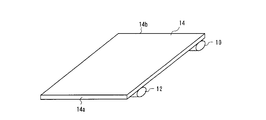
- the electrode layer is formed by sputtering or the like while the substrate 14 on which the photovoltaic layer is formed by the rollers 10 and 12 is conveyed in a direction orthogonal to the extending direction of the rollers 10 and 12.
- the electrode layer is formed so as to wrap around the glass substrate side at the edges 14a and 14b along the conveyance direction of the substrate 14.
- the electrode layer is formed so as to wrap around in this way, it may cause a decrease in the dielectric strength characteristics between the electrode layer and the glass substrate.
- the electrode portion formed near the edge of the substrate is positioned in the vicinity of the metal frame that is the module structure when modularized. As a result, the dielectric strength of the module may be reduced.
- One aspect of the present invention is a method for manufacturing a photovoltaic device comprising one or a plurality of photovoltaic cells in which a first electrode layer, a semiconductor layer, and a second electrode layer are formed on a substrate.
- a voltage is applied between the first portion where the photovoltaic force of the second electrode layer is not obtained and the second portion where the photovoltaic force apart from the first portion of the second electrode layer is not obtained, At least a part of the second electrode layer is removed.
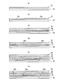
- FIG. 1 It is sectional drawing which shows the manufacturing process of the photovoltaic apparatus in embodiment of this invention. It is a figure explaining the communication session using the transmission / reception apparatus in embodiment of this invention. It is a figure which shows the structure of another example of the transmission / reception apparatus of the communication system in embodiment of this invention. It is a figure which shows arrangement
- a method for manufacturing a photovoltaic device will be described below.
- a tandem thin film photovoltaic device using an amorphous silicon film (a-Si film) and a microcrystalline silicon film ( ⁇ c-Si film) will be described as an example.
- a-Si film amorphous silicon film
- ⁇ c-Si film microcrystalline silicon film
- the application range of the present invention is not limited to this, and can be applied to various photovoltaic devices such as a single layer, a multilayer, a thin film type, and a bulk type.
- a transparent conductive film 22 is formed as a first electrode on the substrate 20 (FIG. 1A).
- a transparent insulating material such as glass or plastic can be used.
- the transparent conductive film 22 is formed of tin oxide (SnO 2), zinc oxide (ZnO), or the like by a thermal chemical vapor deposition method (thermal CVD method) or the like.
- a slit 22a is formed in the transparent conductive film 22 by laser separation processing, and the transparent conductive film 22 is separated into strips (FIG. 1B: the slit 22a is formed in a direction perpendicular to the paper surface).
- the laser separation processing for example, it is preferable to use an Nd: YAG laser having a wavelength of about 1.06 ⁇ m, an energy density of 13 J / cm 3 , and a pulse frequency of 3 kHz.
- a p-layer, an i-layer, and an n-layer are formed on the transparent conductive film 22 in the order of the a-Si film 24 and the ⁇ c-Si film 26 that become the photovoltaic layer (power generation layer), respectively (FIG. 1 ( c)).
- the a-Si film and the ⁇ c-Si film can be formed by a plasma chemical vapor deposition method (P-CVD method). Table 1 shows an example of film formation conditions at this time.
- a laser separation process is performed on the photovoltaic layers 24 and 26 on the side of the slit 22a of the transparent conductive film 22 processed into a strip shape to form a slit 26a, and the photovoltaic layers 24 and 26 are formed into a strip shape.
- a separation process is performed along the slit 22 a of the transparent conductive film 22 at a position 50 ⁇ m away from the slit 22 a of the transparent conductive film 22.
- a metal electrode 28 is formed as a second electrode on the photovoltaic layer 26 (FIG. 1 (e)).
- the metal electrode 28 for example, silver (Ag) is preferably used as a main material.
- the metal electrode 28 can be formed by sputtering.
- the film thickness of the metal electrode 28 is preferably 200 nm, for example.
- the deposit attached to the substrate holder may be taken into the metal electrode 28. Therefore, as shown in FIG. 9, it is preferable to adopt a holderless method (trayless method) in which the metal electrode 28 is formed while the substrate 20 is conveyed by the rollers 10 and 12.
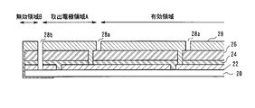
- the metal electrode 28 on the side of the slit 26a of the photovoltaic layer 26 processed into a strip shape is subjected to laser separation processing to form a slit 28a, and the metal electrode 28 is separated into a strip shape (FIG. 1). (F)).
- a position 50 ⁇ m away from the slit 26 a of the photovoltaic layer 26 on the side opposite to the slit 22 a of the transparent conductive film 22 is separated along the slit 26 a of the photovoltaic layer 26.
- a laser separation process is performed in the vicinity of the end portion of the substrate 20 to form a slit 28b.
- the slit 28 b is provided so as to penetrate the transparent conductive film 22, the photovoltaic layers 24 and 26, and the metal electrode 28. By providing the slit 28 b, an ineffective portion that does not contribute to power generation is formed in the end region of the substrate 20.
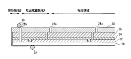
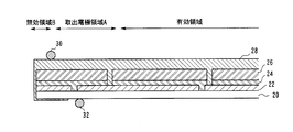
- the metal electrode 28 wraps around the substrate 20 side as shown in the cross-sectional view of the substrate end in FIG. In addition, the metal electrode 28 may be formed even on the surface.
- the electrode rod 30, which is a conductive member, slightly protrudes from the extraction electrode region A of the photovoltaic device, and is disposed at a position in contact with the ineffective region B. Further, another electrode bar 32 is disposed at a position away from the metal electrode 28 that has wrapped around the surface of the substrate 20.
- the electrode rods 30 and 32 may be formed of a conductive member, but for example, copper is preferable. Moreover, since it is desirable that the electrode rods 30 and 32 can be disposed over the side of the substrate 20, the length is preferably equal to or larger than the width of the substrate 20.
- the electrode rods 30 and 32 may be, for example, a columnar shape, a cylindrical shape, or a prismatic shape, but it is more preferable that the electrode rods 30 and 32 have a curved surface that comes into linear contact with the metal electrode 28.
- a voltage is applied between the electrode rods 30 and 32.
- the voltage to be applied is preferably higher than at least the electromotive force of the solar battery cell (photovoltaic cell). That is, it is preferable that the voltage be such that the metal electrode 28 evaporates due to Joule heat generated by the current flowing through the electrode rods 30 and 32.
- the voltage is preferably set to 100 V or more and 5000 V or less.
- a device having a protection circuit that senses the supply current and stops the voltage application when a current larger than a predetermined value flows such as a withstand voltage test device. It is.
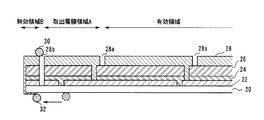
- the electrode rod 32 is moved toward the end of the substrate 20 little by little while making contact with the surface of the substrate 20 or the surface of the metal electrode 28 formed by wrapping around. Thereby, a current flows between the electrode rods 30 and 32, and the metal electrode 28 evaporates due to Joule heat generated by the current.
- the excess metal electrode 28 can be removed. .
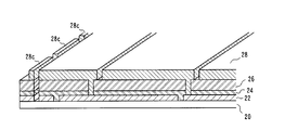
- the electrode rod 32 Since a voltage is applied between the electrode rods 30 and 32, it is preferable to move the electrode rod 32 to such an extent that the electrode rods 30 and 32 do not contact each other. Therefore, as shown in the perspective view of FIG. 6, a part of the surface of the photovoltaic layer 26 is not covered with the metal electrode 28 at the end of the substrate 20 of the photovoltaic device, and the gap between the electrode rods 30 and 32 is not covered. Correspondingly, the metal electrode 28c remains in an island shape, but the withstand voltage of the photovoltaic device can be improved.
- the electrode rod 32 may be fixed and the electrode rod 30 may be moved. Also, both electrode rods 30 and 32 may be moved closer to each other.
- the metal electrode 28 may be removed using laser light instead of applying a high voltage to the electrode rods 30 and 32 to remove the metal electrode 28.
- the metal electrode 28 can be removed using a laser used in forming a thin film solar cell module.
- the substrate 20 is irradiated with laser light from the photovoltaic layer 26 side under conditions of a wavelength of 532 nm, a frequency of 10 kHz, and a power of 0.7 W so that the laser light is scanned so that the irradiation regions of the laser light overlap.
- the metal electrode 28 in an arbitrary region can be removed by moving the electrode vertically and horizontally.
- the metal electrode 28 may be removed by blasting.
- blasting the metal electrode 28 is removed using mechanical energy by blowing fine particles from a nozzle.
- the particles are preferably made of tungsten, alumina, silica, zirconium oxide or the like. It is preferable that the particle size of the abrasive is about # 1000 (# 1000) of an abrasive.
- # 1000 # 1000 of an abrasive. For example, by injecting tungsten particles under conditions of an injection pressure of 0.15 MPa and 80 Hz (68 g / min) and moving the substrate 20 at a relative speed of 1.0 m / min, The metal electrode 28 can be removed.
- the metal electrode 28 may be removed by etching.
- the metal electrode 28 is etched and removed by immersing it in an aqueous solution in which 28% diluted ammonium hydroxide (NH 4 OH) and hydrogen peroxide (H 2 O 2 ) are mixed at a ratio of 2: 1. Is done. It is preferable to protect the region other than the region to be removed by etching with an appropriate resist agent or the like.
- a copper foil lead (not shown) is attached to the extraction electrode portion A formed at the end of the substrate 20 as an extraction electrode by ultrasonic soldering.
- the filling part 40 is formed by sequentially vacuum-pressing EVA / back film (polyethyl terephthalate: PET or the like) with a laminator.
- the back film may be a structure in which a fluorine resin (ETFE, PVDF), PC, glass or the like sandwiches a metal foil, or a single metal or a metal (steel plate) such as stainless steel or galvalume.
- the vacuum thermocompression bonding is preferably performed at 150 ° C., for example.
- a module is completed by attaching a rubber or other cushioning member 46 to a frame 48 of aluminum, iron, stainless steel or the like.
- the pressure resistance test was performed on the module that had been subjected to the removal treatment of the metal electrode 28 and the module that had not been performed in the present embodiment, and the pressure resistance of each module was examined.
- the pressure resistance test was performed according to JIS C 8917.
- the metal electrode 28 is subjected to laser separation processing to form the slit 28a, and then the removal process of the metal electrode 28 is performed.
- the removal process may be performed before the slit 28a is formed. That is, as shown in FIG. 8, the electrode rod 30 is brought into contact with a position that becomes the ineffective region B of the photovoltaic device, and the electrode rod 32 is arranged at a position away from the metal electrode 28 that wraps around the surface of the substrate 20. Then, the electrode rod 32 may be moved gradually while applying a voltage.
- the slit 28a is formed by making a laser incident from the substrate 20 side.
- an unnecessary metal electrode 28 is formed on the edge of the substrate 20, the transparent conductive film 22, the photovoltaic films 24, 26, etc. can be irradiated under the desired conditions by being interrupted by the metal electrode 28. It may not be possible. In such a case, it is preferable to remove unnecessary metal electrodes 28 before forming the slits 28a.
- the case where the removal process of the metal electrode 28 is applied to the end portion on the positive electrode (+ electrode) side of the photovoltaic device has been described, but the end on the negative electrode ( ⁇ electrode) side is shown.
- the treatment can also be applied to the metal electrode 28 at the end in the direction along the slits 22a, 26a, 28a of the substrate or the substrate 20.
- the method of removing the metal electrode 28 that has come to the surface side of the substrate 20 has been described.
- the present embodiment also applies when the metal electrode 28 does not go to the surface side of the substrate 20.
- the metal removal method in can be applied.
- the modularized frame 48 and the photovoltaic device It is possible to improve the withstand voltage characteristic between.
Landscapes
- Photovoltaic Devices (AREA)
Abstract
Description

Claims (7)
- 基板上に第1電極層、半導体層及び第2電極層が形成された1つ又は複数の光起電力セルからなる光起電力装置の製造方法であって、
前記第2電極層の光起電力が得られない第1部位と、前記第2電極層の前記第1部位から離れた光起電力が得られない第2部位と、の間に電圧を印加し、前記第2電極層の少なくとも一部を除去することを特徴とする光起電力装置の製造方法。 - 請求項1に記載の光起電力装置の製造方法であって、
前記第1部位は、前記半導体層側に形成された前記第2電極層の部位であり、
前記第2部位は、前記半導体層と反対に回り込んだ前記第2電極層の部位であり、
前記第2部位の少なくとも一部を除去することを特徴とする光起電力装置の製造方法。 - 請求項1に記載の光起電力装置の製造方法であって、
前記電圧を印加する際に、前記第1部位に電圧を印加する電極及び前記第2部位に電圧を印加する電極の少なくとも一方を移動させながら電圧を印加することを特徴とする光起電力装置の製造方法。 - 請求項1に記載の光起電力装置の製造方法であって、
前記電圧は、少なくとも前記光起電力セルの起電力よりも高いことを特徴とする光起電力装置の製造方法。 - 請求項1に記載の光起電力装置の製造方法であって、
前記電圧の印加は棒状の導電性部材を用いることを特徴とする光起電力装置の製造方法。 - 基板上に第1電極層、半導体層及び第2電極層が形成された1つ又は複数の光起電力セルからなる光起電力装置であって、
前記半導体層の一部が前記第2電極層によって被われていないことを特徴とする光起電力装置。 - 請求項6に記載の光起電力装置であって、
前記基板端部における前記半導体層上の前記第2電極層が島状に形成されていることを特徴とする光起電力装置。
Priority Applications (3)
| Application Number | Priority Date | Filing Date | Title |
|---|---|---|---|
| JP2010504978A JPWO2010029880A1 (ja) | 2008-09-10 | 2009-09-02 | 光起電力装置及び光起電力装置の製造方法 |
| CN2009801005777A CN101809760B (zh) | 2008-09-10 | 2009-09-02 | 光电装置和光电装置的制造方法 |
| US12/679,605 US20100200042A1 (en) | 2008-09-10 | 2009-09-02 | Photovoltaic device and method for manufacturing photovoltaic device |
Applications Claiming Priority (2)
| Application Number | Priority Date | Filing Date | Title |
|---|---|---|---|
| JP2008-231951 | 2008-09-10 | ||
| JP2008231951 | 2008-09-10 |
Publications (1)
| Publication Number | Publication Date |
|---|---|
| WO2010029880A1 true WO2010029880A1 (ja) | 2010-03-18 |
Family
ID=42005137
Family Applications (1)
| Application Number | Title | Priority Date | Filing Date |
|---|---|---|---|
| PCT/JP2009/065340 Ceased WO2010029880A1 (ja) | 2008-09-10 | 2009-09-02 | 光起電力装置及び光起電力装置の製造方法 |
Country Status (5)
| Country | Link |
|---|---|
| US (1) | US20100200042A1 (ja) |
| JP (1) | JPWO2010029880A1 (ja) |
| KR (1) | KR20100051721A (ja) |
| CN (1) | CN101809760B (ja) |
| WO (1) | WO2010029880A1 (ja) |
Cited By (1)
| Publication number | Priority date | Publication date | Assignee | Title |
|---|---|---|---|---|
| WO2023189906A1 (ja) * | 2022-03-31 | 2023-10-05 | 株式会社カネカ | 太陽電池モジュール |
Families Citing this family (1)
| Publication number | Priority date | Publication date | Assignee | Title |
|---|---|---|---|---|
| TWI521725B (zh) * | 2013-04-22 | 2016-02-11 | 茂迪股份有限公司 | 太陽能電池之製造方法 |
Citations (2)
| Publication number | Priority date | Publication date | Assignee | Title |
|---|---|---|---|---|
| JP2005268466A (ja) * | 2004-03-18 | 2005-09-29 | Sanyo Electric Co Ltd | 光起電力装置 |
| JP2007103434A (ja) * | 2005-09-30 | 2007-04-19 | Sharp Corp | 太陽電池素子 |
Family Cites Families (5)
| Publication number | Priority date | Publication date | Assignee | Title |
|---|---|---|---|---|
| JPS603164A (ja) * | 1983-06-21 | 1985-01-09 | Sanyo Electric Co Ltd | 光起電力装置の製造方法 |
| US4542255A (en) * | 1984-01-03 | 1985-09-17 | Atlantic Richfield Company | Gridded thin film solar cell |
| JP4201241B2 (ja) * | 2001-05-17 | 2008-12-24 | 株式会社カネカ | 集積型薄膜光電変換モジュールの作製方法 |
| JP2003069064A (ja) * | 2001-08-28 | 2003-03-07 | Fuji Electric Co Ltd | 太陽電池モジュールとその製造方法 |
| JP4762100B2 (ja) * | 2006-09-28 | 2011-08-31 | 三洋電機株式会社 | 太陽電池モジュール |
-
2009
- 2009-09-02 WO PCT/JP2009/065340 patent/WO2010029880A1/ja not_active Ceased
- 2009-09-02 US US12/679,605 patent/US20100200042A1/en not_active Abandoned
- 2009-09-02 KR KR1020107005495A patent/KR20100051721A/ko not_active Abandoned
- 2009-09-02 CN CN2009801005777A patent/CN101809760B/zh not_active Expired - Fee Related
- 2009-09-02 JP JP2010504978A patent/JPWO2010029880A1/ja active Pending
Patent Citations (2)
| Publication number | Priority date | Publication date | Assignee | Title |
|---|---|---|---|---|
| JP2005268466A (ja) * | 2004-03-18 | 2005-09-29 | Sanyo Electric Co Ltd | 光起電力装置 |
| JP2007103434A (ja) * | 2005-09-30 | 2007-04-19 | Sharp Corp | 太陽電池素子 |
Cited By (1)
| Publication number | Priority date | Publication date | Assignee | Title |
|---|---|---|---|---|
| WO2023189906A1 (ja) * | 2022-03-31 | 2023-10-05 | 株式会社カネカ | 太陽電池モジュール |
Also Published As
| Publication number | Publication date |
|---|---|
| KR20100051721A (ko) | 2010-05-17 |
| US20100200042A1 (en) | 2010-08-12 |
| JPWO2010029880A1 (ja) | 2012-02-02 |
| CN101809760A (zh) | 2010-08-18 |
| CN101809760B (zh) | 2012-06-06 |
Similar Documents
| Publication | Publication Date | Title |
|---|---|---|
| US20110124151A1 (en) | Photovoltaic device and method for manufacturing the same | |
| WO2008050556A1 (fr) | Cellule solaire à film mince et son procédé de fabrication | |
| CN104011882A (zh) | 制造太阳能电池装置的方法 | |
| JP6909267B2 (ja) | 光電変換装置の製造方法 | |
| US10388821B2 (en) | Method for manufacturing crystalline silicon-based solar cell and method for manufacturing crystalline silicon-based solar cell module | |
| WO2008038553A1 (fr) | Module de cellules solaires | |
| CN118866999A (zh) | 用于太阳能电池电路形成的激光辅助金属化工艺 | |
| CN101779294B (zh) | 光电转换装置 | |
| CN102113127B (zh) | 光电转换装置 | |
| TWI435453B (zh) | A photoelectric conversion device, and a method of manufacturing the photoelectric conversion device | |
| TW201019494A (en) | Photoelectric conversion device manufacturing method and photoelectric conversion device | |
| JPWO2010029880A1 (ja) | 光起電力装置及び光起電力装置の製造方法 | |
| CN102414842A (zh) | 光电转换装置的制造方法 | |
| JP5030745B2 (ja) | 光電変換装置の製造方法 | |
| JP2006222192A (ja) | 光起電力装置、光起電力モジュールおよびその製造方法 | |
| CN101755340B (zh) | 光电转换装置及其制造方法 | |
| CN102197493B (zh) | 光电转换装置的制造方法及制膜装置 | |
| CN102473757A (zh) | 光电转换装置的制造方法 | |
| JP2011066213A (ja) | 光電変換装置及びその製造方法 | |
| JP4162373B2 (ja) | 光起電力装置の製造方法 | |
| CN103081116A (zh) | 光电转换装置的制造方法 | |
| CN101765922A (zh) | 光电转换装置的制造方法及光电转换装置 | |
| JP5123871B2 (ja) | 光電変換装置の製造方法 | |
| JP2010199305A (ja) | 光電変換装置の製造方法 |
Legal Events
| Date | Code | Title | Description |
|---|---|---|---|
| WWE | Wipo information: entry into national phase |
Ref document number: 200980100577.7 Country of ref document: CN |
|
| WWE | Wipo information: entry into national phase |
Ref document number: 2010504978 Country of ref document: JP |
|
| ENP | Entry into the national phase |
Ref document number: 20107005495 Country of ref document: KR Kind code of ref document: A |
|
| WWE | Wipo information: entry into national phase |
Ref document number: 12679605 Country of ref document: US |
|
| 121 | Ep: the epo has been informed by wipo that ep was designated in this application |
Ref document number: 09813026 Country of ref document: EP Kind code of ref document: A1 |
|
| NENP | Non-entry into the national phase |
Ref country code: DE |
|
| 122 | Ep: pct application non-entry in european phase |
Ref document number: 09813026 Country of ref document: EP Kind code of ref document: A1 |