WO2010026830A1 - 表示装置 - Google Patents
表示装置 Download PDFInfo
- Publication number
- WO2010026830A1 WO2010026830A1 PCT/JP2009/062354 JP2009062354W WO2010026830A1 WO 2010026830 A1 WO2010026830 A1 WO 2010026830A1 JP 2009062354 W JP2009062354 W JP 2009062354W WO 2010026830 A1 WO2010026830 A1 WO 2010026830A1
- Authority
- WO
- WIPO (PCT)
- Prior art keywords
- wiring
- signal
- output
- potential
- display device
- Prior art date
Links
Images


Classifications
-
- G—PHYSICS
- G06—COMPUTING; CALCULATING OR COUNTING
- G06F—ELECTRIC DIGITAL DATA PROCESSING
- G06F3/00—Input arrangements for transferring data to be processed into a form capable of being handled by the computer; Output arrangements for transferring data from processing unit to output unit, e.g. interface arrangements
- G06F3/01—Input arrangements or combined input and output arrangements for interaction between user and computer
- G06F3/03—Arrangements for converting the position or the displacement of a member into a coded form
- G06F3/041—Digitisers, e.g. for touch screens or touch pads, characterised by the transducing means
- G06F3/0412—Digitisers structurally integrated in a display
-
- G—PHYSICS
- G06—COMPUTING; CALCULATING OR COUNTING
- G06F—ELECTRIC DIGITAL DATA PROCESSING
- G06F3/00—Input arrangements for transferring data to be processed into a form capable of being handled by the computer; Output arrangements for transferring data from processing unit to output unit, e.g. interface arrangements
- G06F3/01—Input arrangements or combined input and output arrangements for interaction between user and computer
- G06F3/03—Arrangements for converting the position or the displacement of a member into a coded form
- G06F3/041—Digitisers, e.g. for touch screens or touch pads, characterised by the transducing means
- G06F3/042—Digitisers, e.g. for touch screens or touch pads, characterised by the transducing means by opto-electronic means
-
- G—PHYSICS
- G09—EDUCATION; CRYPTOGRAPHY; DISPLAY; ADVERTISING; SEALS
- G09G—ARRANGEMENTS OR CIRCUITS FOR CONTROL OF INDICATING DEVICES USING STATIC MEANS TO PRESENT VARIABLE INFORMATION
- G09G3/00—Control arrangements or circuits, of interest only in connection with visual indicators other than cathode-ray tubes
- G09G3/20—Control arrangements or circuits, of interest only in connection with visual indicators other than cathode-ray tubes for presentation of an assembly of a number of characters, e.g. a page, by composing the assembly by combination of individual elements arranged in a matrix no fixed position being assigned to or needed to be assigned to the individual characters or partial characters
- G09G3/34—Control arrangements or circuits, of interest only in connection with visual indicators other than cathode-ray tubes for presentation of an assembly of a number of characters, e.g. a page, by composing the assembly by combination of individual elements arranged in a matrix no fixed position being assigned to or needed to be assigned to the individual characters or partial characters by control of light from an independent source
- G09G3/36—Control arrangements or circuits, of interest only in connection with visual indicators other than cathode-ray tubes for presentation of an assembly of a number of characters, e.g. a page, by composing the assembly by combination of individual elements arranged in a matrix no fixed position being assigned to or needed to be assigned to the individual characters or partial characters by control of light from an independent source using liquid crystals
- G09G3/3611—Control of matrices with row and column drivers
- G09G3/3648—Control of matrices with row and column drivers using an active matrix
-
- G—PHYSICS
- G09—EDUCATION; CRYPTOGRAPHY; DISPLAY; ADVERTISING; SEALS
- G09G—ARRANGEMENTS OR CIRCUITS FOR CONTROL OF INDICATING DEVICES USING STATIC MEANS TO PRESENT VARIABLE INFORMATION
- G09G3/00—Control arrangements or circuits, of interest only in connection with visual indicators other than cathode-ray tubes
- G09G3/20—Control arrangements or circuits, of interest only in connection with visual indicators other than cathode-ray tubes for presentation of an assembly of a number of characters, e.g. a page, by composing the assembly by combination of individual elements arranged in a matrix no fixed position being assigned to or needed to be assigned to the individual characters or partial characters
- G09G3/34—Control arrangements or circuits, of interest only in connection with visual indicators other than cathode-ray tubes for presentation of an assembly of a number of characters, e.g. a page, by composing the assembly by combination of individual elements arranged in a matrix no fixed position being assigned to or needed to be assigned to the individual characters or partial characters by control of light from an independent source
- G09G3/36—Control arrangements or circuits, of interest only in connection with visual indicators other than cathode-ray tubes for presentation of an assembly of a number of characters, e.g. a page, by composing the assembly by combination of individual elements arranged in a matrix no fixed position being assigned to or needed to be assigned to the individual characters or partial characters by control of light from an independent source using liquid crystals
- G09G3/3611—Control of matrices with row and column drivers
- G09G3/3685—Details of drivers for data electrodes
- G09G3/3688—Details of drivers for data electrodes suitable for active matrices only
-
- G—PHYSICS
- G02—OPTICS
- G02F—OPTICAL DEVICES OR ARRANGEMENTS FOR THE CONTROL OF LIGHT BY MODIFICATION OF THE OPTICAL PROPERTIES OF THE MEDIA OF THE ELEMENTS INVOLVED THEREIN; NON-LINEAR OPTICS; FREQUENCY-CHANGING OF LIGHT; OPTICAL LOGIC ELEMENTS; OPTICAL ANALOGUE/DIGITAL CONVERTERS
- G02F1/00—Devices or arrangements for the control of the intensity, colour, phase, polarisation or direction of light arriving from an independent light source, e.g. switching, gating or modulating; Non-linear optics
- G02F1/01—Devices or arrangements for the control of the intensity, colour, phase, polarisation or direction of light arriving from an independent light source, e.g. switching, gating or modulating; Non-linear optics for the control of the intensity, phase, polarisation or colour
- G02F1/13—Devices or arrangements for the control of the intensity, colour, phase, polarisation or direction of light arriving from an independent light source, e.g. switching, gating or modulating; Non-linear optics for the control of the intensity, phase, polarisation or colour based on liquid crystals, e.g. single liquid crystal display cells
- G02F1/133—Constructional arrangements; Operation of liquid crystal cells; Circuit arrangements
- G02F1/13306—Circuit arrangements or driving methods for the control of single liquid crystal cells
- G02F1/13312—Circuits comprising photodetectors for purposes other than feedback
-
- G—PHYSICS
- G09—EDUCATION; CRYPTOGRAPHY; DISPLAY; ADVERTISING; SEALS
- G09G—ARRANGEMENTS OR CIRCUITS FOR CONTROL OF INDICATING DEVICES USING STATIC MEANS TO PRESENT VARIABLE INFORMATION
- G09G2360/00—Aspects of the architecture of display systems
- G09G2360/14—Detecting light within display terminals, e.g. using a single or a plurality of photosensors
- G09G2360/144—Detecting light within display terminals, e.g. using a single or a plurality of photosensors the light being ambient light
-
- G—PHYSICS
- G09—EDUCATION; CRYPTOGRAPHY; DISPLAY; ADVERTISING; SEALS
- G09G—ARRANGEMENTS OR CIRCUITS FOR CONTROL OF INDICATING DEVICES USING STATIC MEANS TO PRESENT VARIABLE INFORMATION
- G09G2360/00—Aspects of the architecture of display systems
- G09G2360/14—Detecting light within display terminals, e.g. using a single or a plurality of photosensors
- G09G2360/145—Detecting light within display terminals, e.g. using a single or a plurality of photosensors the light originating from the display screen
- G09G2360/147—Detecting light within display terminals, e.g. using a single or a plurality of photosensors the light originating from the display screen the originated light output being determined for each pixel
- G09G2360/148—Detecting light within display terminals, e.g. using a single or a plurality of photosensors the light originating from the display screen the originated light output being determined for each pixel the light being detected by light detection means within each pixel
Definitions
- the present invention relates to a display device with a photosensor having a photodetection element such as a photodiode or phototransistor, and more particularly to a display device having a photosensor in a pixel region.
- a photodetection element such as a photodiode or phototransistor
- a display device with a photosensor that can detect the brightness of external light or capture an image of an object close to the display by providing a photodetection element such as a photodiode in the pixel.
- a display device with an optical sensor is assumed to be used as a display device for bidirectional communication or a display device with a touch panel function.
- a well-known component such as a signal line, a scanning line, a TFT (Thin Film Transistor), and a pixel electrode is formed by a semiconductor process on the active matrix substrate, simultaneously on the active matrix substrate.
- a photodiode or the like is built in (see, for example, Patent Document 1).
- FIG. 25 An example of a conventional optical sensor (for example, see Patent Documents 2 and 3) formed on an active matrix substrate is shown in FIG.
- the conventional optical sensor shown in FIG. 25 includes a photodiode D1, a capacitor C2, and a transistor M2.
- a wiring for supplying a reset signal RS is connected to the anode of the photodiode D1.
- One of the electrodes of the capacitor C2 and the gate of the transistor M2 are connected to the cathode of the photodiode D1.
- the drain of the transistor M2 is connected to a wiring that supplies a constant voltage Vsup.
- sensor circuit output data SData of the optical sensor is output from the source of the transistor M2.
- the other electrode of the capacitor C2 is connected to a wiring for supplying a read signal RW.
- the sensor circuit output data SData corresponding to the amount of light received by the photodiode D1 can be obtained by supplying the reset signal RS and the read signal RW at predetermined timings.
- the low level (for example, ⁇ 4 V) of the reset signal RS is represented as ⁇ V b
- the high level (for example, 8 V) of the read signal RW is represented as V rw . Note that the high level of the reset signal RS is 0V, and the low level of the read signal RW is 0V.
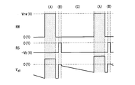
- the sensing sequence of the optical sensor shown in FIG. 25 will be described in three parts: (A) a readout period, (B) a reset period, and (C) a sensing period.
- the transistor M2 When the pulled-up potential V INT exceeds the threshold value of the transistor M2, the transistor M2 is turned on and sensor data SData is output. At this time, the potential V out of SData can threshold V th of the transistors M2, the current value of the constant current source I, when the conductance of the transistor M2 beta, V out ⁇ V INT ⁇ V th ⁇ (2I / ⁇ ) 1/2 It can be expressed as.
- (C) Sensing period starts when the reset signal returns from the high level to the low level. That is, as described above, after the storage node is reset during the reset period, the reset signal RS becomes low level ( ⁇ V b ), thereby generating a reverse bias in the photodiode D1. Then, the optical current corresponding to the amount of incident light to the photodiode D1, the storage node changes to the -V b direction.
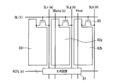
- FIG. 27 shows a configuration example of the photosensor in the pixel.
- one sensor circuit 81 is provided for one pixel composed of three color picture elements of red (r), green (g), and blue (b).
- the sensor circuit 81 corresponds to the photodiode D1, the capacitor C2, and the transistor M2 in the configuration shown in FIG.
- the gate lines GL and the source lines SL are arranged in a matrix, and the TFT 83 for driving the pixel electrodes 82r, 82g, and 82b of each picture element at the intersection of the gate lines GL and the source lines SL. Is provided.
- the gate of the TFT 83 is connected to the gate line GL, the source is connected to the source line SL, and the drain is connected to the pixel electrodes 82r, 82g, and 82b.
- the pixel electrodes 82r, 82g, and 82b are repeatedly arranged along the row direction with these three as one unit.
- L gate lines GL are provided on the matrix substrate. That is, the number of pixels in the row direction on this matrix substrate is L.
- the gate lines GL need to be individually distinguished, they are represented as GL (l) (l is a natural number from 1 to L).
- the source lines SL are provided as M sets (that is, 3M lines) on the matrix substrate, with the source lines SLr, SLg, and SLb as one set. That is, the number of pixels in the column direction (horizontal direction) on this matrix substrate is M, and the number of picture elements is 3M.
- SLr (m) when it is necessary to individually distinguish the source lines SL, they are expressed as SLr (m), SLg (m), SLb (m). That is, m is a natural number from 1 to M.
- N wirings for supplying the above-described reset signal RS and readout signal RW to the sensor circuit 81 are laid as a control signal line group RCTL for driving the sensor circuit 81.
- N may be equal to the number L of the gate lines GL or may be smaller than L.
- N L.
- N L / 2. It becomes.
- the power supply line Vsup that supplies power to the sensor circuit 81 is laid between the source lines SLg (m) and SLb (m).
- An output wiring SData for outputting data from the sensor circuit 81 is laid between the source lines SLr (m) and SLg (m).
- any of the source lines SL may serve as the power supply line Vsup and the output wiring SData.
- the sensor drive must be executed in a period (for example, a blanking period) in which the source line SL is not used in the video display operation.
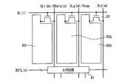
- the aperture ratio is high. That is, in the configuration shown in FIG. 28, the video signal is applied to the source line SL during the video display operation.
- a constant voltage is supplied from the power source to the source line SLg (m) by switching the switch, so that the source line functions as the power source line Vsup.
- sensor circuit output data is output from the sensor circuit 81 to the source line SLr (m) by switching the switch.
- this source line functions as the output wiring SData during sensor driving.
- the storage node (the connection point between the cathode of the photodiode and the capacitor), the power supply line Vsup for supplying power to the sensor circuit 81, and the output wiring SData
- the parasitic capacitances Cps and Cpd are parasitic capacitances. For this reason, if the potentials of these wirings fluctuate between when the sensor circuit 81 is reset and read out, the potential difference is propagated to the storage node via the parasitic capacitance, thereby changing the potential V INT of the storage node. It becomes. As a result, there is a problem that offset noise occurs in the output from the sensor circuit 81.
- FIG. 29 As shown in FIG. 27, in the configuration in which the power supply line Vsup and the output wiring SData are provided independently of the source line SL, only the sensor circuit 81 and a wiring group necessary for driving the sensor circuit 81 are extracted. It is the equivalent circuit diagram shown. As shown in FIG. 29, in this configuration, the power supply line Vsup and the output wiring SData are common to all the sensor circuits 81 arranged in the same column.
- Noise_SD Cps / Ctotal / V_SData (1)
- the sensor circuit output data that is read out to the output wiring SData Is affected by the potential of the output wiring SData immediately before the read signal RW and the reset signal RS (Vs1, Vw2, Vs2,... Shown in FIG. 30) and fluctuates. Note that the potentials Vs1, Vw2, Vs2,... Of the output wiring SData depend on the potential of the sensor circuit output data immediately before.
- the light enters the photodiode D1 during each sensing period. Even if the amount of light to be applied is the same, the following offset Voff2-3 occurs due to the parasitic capacitance. This is obtained from the above equation (1).
- Voff2-3 Cps / Ctotal ⁇ ⁇ (Vs1 ⁇ Vw2) ⁇ (Vs2 ⁇ Vw3) ⁇ Further, between the sensor circuit output data read by the pulse 3 of the read signal RW and the sensor circuit output data read by the pulse 4 of the read signal RW, the amount of light incident on the photodiode D1 is the same during each sensing period. Even if, the following offset Voff3-4 occurs due to the parasitic capacitance.
- Voff3-4 Cps / Ctotal ⁇ ⁇ (Vs2-Vw3)-(Vs3-Vw4) ⁇
- the potentials Vs1, Vw2, Vs2,. . Therefore, the offset Voff2-3 and the offset Voff3-4 are not necessarily constant.
- the sensor circuit output data has an offset caused by the potential fluctuation of the output wiring SData immediately before the read signal RW and the reset signal RS even if the amount of light incident on the photodiode D1 is constant. Further, as described above, since this offset is not constant, it cannot be simply removed.
- an object of the present invention is to provide a display device with an optical sensor capable of obtaining highly accurate sensor circuit output data by eliminating an offset of an accumulation node caused by parasitic capacitance. .
- a display device is a display device including a photosensor in a pixel region of an active matrix substrate, and the photosensor receives a light detection element; A storage node connected to the photodetecting element, the potential of which changes depending on an output current from the photodetecting element, a reset signal wiring for supplying a reset signal to the photosensor, and a read signal for supplying a read signal to the photosensor A sensing period is defined between the wiring and the supply of the readout signal after the reset signal is supplied, and the potential of the storage node that changes according to the amount of light received by the light detection element during the sensing period A sensor switching element for reading out to the output wiring as an output, immediately before the readout signal, and the reset In at least one of the immediately preceding item, characterized by fixing the potential of the wiring having a parasitic capacitance between the storage node to a predetermined potential.
- FIG. 1 is a block diagram showing a schematic configuration of a display device according to an embodiment of the present invention.
- FIG. 2 is an equivalent circuit diagram showing a configuration of one pixel in the display device according to the embodiment of the present invention.
- FIG. 3 is an equivalent circuit diagram illustrating a configuration example of the row driver.
- FIG. 4 is a timing chart of signals related to driving of the row driver.
- FIG. 5 is an equivalent circuit diagram showing a configuration example of the column driver.
- FIG. 6 is a timing chart of signals related to driving of the column driver.
- FIG. 7 is an equivalent circuit diagram illustrating a configuration example of the gate driver.
- FIG. 8 is a timing chart of signals related to driving of the gate driver.
- FIG. 9 is an equivalent circuit diagram illustrating a configuration example of the source driver.
- FIG. 9 is an equivalent circuit diagram illustrating a configuration example of the source driver.
- FIG. 10 is a timing chart of signals related to driving of the source driver.
- FIG. 11 is an equivalent circuit diagram illustrating a configuration example of the source driver and the column driver.
- FIG. 12 is a timing chart showing the relationship between display operation timing and sensing timing.
- FIG. 13 is a timing chart of sensor drive signals in the first embodiment.
- FIG. 14 is an equivalent circuit diagram showing the configuration of the column driver in the first embodiment.
- FIG. 15 is a timing chart showing the relationship between the read signal, the reset signal, the discharge signal, and the potential of the data output wiring.
- FIG. 16 is an equivalent circuit diagram showing a configuration of one pixel in the display device according to the embodiment of the present invention.
- FIG. 17 is a timing chart showing the relationship between display operation timing and sensing timing.
- FIG. 18 is a timing chart of sensor drive signals in the second embodiment.
- FIG. 19 is an equivalent circuit diagram showing the configuration of the column driver in the second embodiment.
- FIG. 20 is a timing chart of sensor drive signals in the third embodiment.
- FIG. 21 is an equivalent circuit diagram showing the configuration of the differential amplifier circuit of the source driver in the third embodiment.
- (A) is an equivalent circuit diagram which shows the structure of the differential amplifier circuit of the source driver in 3rd Embodiment
- (b) is a timing chart of the drive signal of the circuit of (a).
- FIG. 23 is a timing chart of sensor drive signals in the fourth embodiment.
- FIG. 24 is an equivalent circuit diagram of another embodiment of a sensor circuit to which the present invention is applicable.
- FIG. 25 is an equivalent circuit diagram showing an example of a conventional photosensor formed on an active matrix substrate.
- FIG. 26 is a timing chart showing the waveform of the drive signal in the conventional optical sensor.
- FIG. 27 is a schematic diagram showing an example of wiring in a conventional optical sensor.
- FIG. 28 is a schematic diagram showing another example of wiring in a conventional optical sensor.
- FIG. 29 is an equivalent circuit diagram showing a connection relationship between the optical sensor circuit and peripheral wiring.
- FIG. 30 is a timing chart for explaining a state in which the potential of the data read wiring changes immediately before the read signal and immediately before the reset signal.
- a display device is a display device that includes a photosensor in a pixel region of an active matrix substrate, and the photosensor includes a photodetection element that receives incident light, and a photodetection element.
- the period from when the signal is supplied to when the readout signal is supplied is defined as a sensing period, and the potential of the storage node that changes according to the amount of light received by the light detection element during the sensing period is output to the output wiring as a sensor circuit output.
- the potential of the wiring having a parasitic capacitance between the storage node and the storage node is fixed to a predetermined potential at least one of immediately before the read signal and immediately before the reset signal. It is possible to prevent the potential of the storage node from fluctuating due to a potential variation caused by a wiring potential just before reading and / or just before resetting. As a result, it is possible to provide a display device with an optical sensor that eliminates the offset of the storage node caused by the parasitic capacitance and obtains highly accurate sensor circuit output data.
- the wiring having parasitic capacitance with the storage node is the output wiring.
- the potential of the output wiring varies depending on the level of the immediately preceding sensor circuit output data or the level of the immediately preceding video signal or the like depending on the circuit configuration. Moreover, the magnitude of the fluctuation cannot be predicted. Therefore, by fixing the potential of this wiring to a predetermined potential at least one of immediately before the read signal and immediately before the reset signal, the storage node offset due to the parasitic capacitance can be eliminated. Further, in this configuration, in order to fix the output wiring at the predetermined potential, it is preferable to supply a video signal of a predetermined level to the wiring.
- a wiring having a parasitic capacitance with the storage node is a power wiring that supplies a power supply voltage to the photosensor during a period in which the readout signal is supplied, and the power wiring is a pixel in the pixel region. It is also preferable to have a configuration that also serves as a source line for supplying a video signal. In this configuration, the potential of the power supply wiring varies depending on the level of the video signal supplied to the pixel. Moreover, the magnitude of the fluctuation cannot be predicted. Therefore, the storage node offset due to the parasitic capacitance can be eliminated by fixing the potential of the power supply wiring to a predetermined potential at least one of immediately before the read signal and immediately before the reset signal. Further, in this configuration, it is preferable that the fixing of the power supply wiring to the predetermined potential is controlled by a signal different from the read signal.
- a video signal of a predetermined level is supplied to the wiring, and the output wiring is connected to the first wiring immediately before the reset signal.
- the display device of the present invention can be suitably implemented as a liquid crystal display device further comprising a counter substrate facing the active matrix substrate and a liquid crystal sandwiched between the active matrix substrate and the counter substrate.
- the display device according to the present invention is implemented as a liquid crystal display device.
- the display device according to the present invention is not limited to the liquid crystal display device, and is an active matrix.
- the present invention can be applied to any display device using a substrate.
- the display device according to the present invention includes a touch panel display device that performs an input operation by detecting an object close to the screen by using an optical sensor, and a display for bidirectional communication including a display function and an imaging function. Use as a device is assumed.
- each drawing referred to below shows only the main members necessary for explaining the present invention in a simplified manner among the constituent members of the embodiment of the present invention for convenience of explanation. Therefore, the display device according to the present invention can include arbitrary constituent members that are not shown in the drawings referred to in this specification. Moreover, the dimension of the member in each figure does not represent the dimension of an actual structural member, the dimension ratio of each member, etc. faithfully.
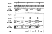
- FIG. 1 is a block diagram showing a schematic configuration of an active matrix substrate 100 provided in a liquid crystal display device according to an embodiment of the present invention.
- an active matrix substrate 100 includes a pixel region 1, a gate driver 2, a source driver 3, a column driver 4, and a row driver on a glass substrate. 5 at least.
- a signal processing circuit for processing an image signal captured by a light detection element (described later) in the pixel region 1 is connected to the active matrix substrate 100 via the FPC 6. .
- the gate driver 2 and the source driver 3 perform scanning for writing a video signal similarly input from the outside to the display pixels in the pixel region 1 in accordance with a synchronization signal (Vsync, Hsync) input from the outside.
- the column driver 4 and the row driver 5 supply various signals (a readout signal and a reset signal, which will be described later) necessary for driving the sensor to the photosensors in the pixel region 1 and read out sensor circuits.
- a driver for sequentially outputting output data to the outside of the display device.
- the arrangement of the various drivers shown in FIG. 1 is merely an example, and how to mount the various drivers is an arbitrary design matter.
- the above-described constituent members on the active matrix substrate 100 can be formed monolithically on the glass substrate by a semiconductor process. Or it is good also as a structure which mounted the amplifier and drivers among said structural members on the glass substrate by COG (Chip On Glass) technique etc., for example.
- COG Chip On Glass
- at least a part of the above-described constituent members shown on the active matrix substrate 100 in FIG. 1 may be mounted on the FPC.
- the active matrix substrate 100 is bonded to a counter substrate (not shown) having a counter electrode formed on the entire surface, and a liquid crystal material is sealed in the gap.
- the pixel area 1 is an area where a plurality of pixels are formed in order to display an image.
- an optical sensor (sensor circuit 81) for capturing an image is provided in each pixel in the pixel region 1.
- FIG. 2 is an equivalent circuit diagram showing the arrangement of the pixels and the sensor circuit 81 in the pixel region 1.
- one pixel is formed by three color picture elements of R (red), G (green), and B (blue), and in one pixel configured by these three picture elements, photo One sensor circuit 81 including a diode D1, a capacitor C2, and a thin film transistor M2 is provided.
- the pixel region 1 includes pixels arranged in a matrix of L rows ⁇ M columns and sensor circuits 81 arranged in a matrix of N rows ⁇ O columns.
- the number (L) of the gate lines GL in the row direction is equal to the number (N) of the sensor circuits 81 in the row direction
- the number of pixels (M) in the column direction is the column direction of the sensor circuits 81. Is equal to the number (O) of The total number of picture elements in the pixel area 1 is (L ⁇ 3M).
- the pixel region 1 has gate lines GL and source lines SL arranged in a matrix as pixel wiring.
- the gate line GL is connected to the gate driver 2.
- the source line SL is connected to the source driver 3.
- the gate lines GL are provided in L rows in the pixel region 1.
- GL (l) is a natural number of 1 to L.
- three source lines SL are provided for each pixel in order to supply image data to three picture elements in one pixel.
- the source lines SL need to be described separately, they are expressed as SLr (m), SLg (m), SLb (m).
- m is a natural number from 1 to M.
- a thin film transistor (TFT) M1 is provided as a switching element for the pixel at the intersection of the gate line GL and the source line SL.
- the thin film transistor M1 provided in each of the red, green, and blue picture elements is denoted as M1r, M1g, and M1b.
- the thin film transistor M1 has a gate electrode connected to the gate line GL, a source electrode connected to the source line SL, and a drain electrode connected to a pixel electrode (not shown).
- a liquid crystal capacitor CLC is formed between the drain electrode of the thin film transistor M1 and the counter electrode (VCOM).
- an auxiliary capacitor C1 is formed between the drain electrode and the TFTCOM.
- the pixel driven by the thin film transistor M1r connected to the intersection of one gate line GL and one source line SLr is provided with a red color filter so as to correspond to this pixel.
- red image data is supplied from the source driver 3 via the source line SLr, it functions as a red picture element.
- a picture element driven by the thin film transistor M1g connected to the intersection of the gate line GL and the source line SLg is provided with a green color filter so as to correspond to the picture element, and a source driver is provided via the source line SLg.
- green image data is supplied from 3 it functions as a green picture element.
- the pixel driven by the thin film transistor M1b connected to the intersection of the gate line GL and the source line SLb is provided with a blue color filter so as to correspond to the pixel, and the source driver is connected via the source line SLb.
- blue image data is supplied from 3, it functions as a blue picture element.
- the power supply line Vsup for supplying power to the sensor circuit 81 and the output wiring SData for outputting sensor circuit output data are provided separately from the source line SL. That is, the drain of the thin film transistor M2 of the sensor circuit 81 is connected to the power supply line Vsup, and the source is connected to the output wiring SData.
- the sensor circuit 81 is provided in the pixel region 1 at a rate of one for each pixel (three picture elements).
- the arrangement ratio of the pixel and the sensor circuit 81 is not limited to this example and is arbitrary.
- one sensor circuit 81 may be arranged for each picture element, or one sensor circuit 81 may be arranged for a plurality of pixels.
- the sensor circuit 81 may be arranged every other row.
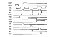
- the row driver 5 starts the RWSP with a shift register 51 including N flip-flops that sequentially generate and transfer a signal in synchronization with the clock signal RCK using the RSSP as a start pulse signal. It has a shift register 52 composed of N flip-flops that sequentially generate and transfer a pulse signal in synchronization with the clock signal RCK.
- the reset signal analog switch RSn and the readout signal analog switch RWn are sequentially controlled to open and close, whereby the reset signal RS and the readout signal RW are respectively transmitted to the sensor circuit 81 disposed in the pixel region 1.
- the shift register 51 for reset signal control and the shift register 52 for read signal control are provided independently, so that the read and reset are performed by changing the timings of the respective start pulses RSSP and RWSP. Can be controlled independently.
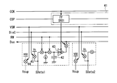
- the column driver 4 includes a shift register 41 composed of O flip-flops, a holding capacitor 42, an output circuit 43, and an analog switch 44.
- the shift register 41 sequentially generates and transfers signals in synchronization with the clock signal CCK using the CSP as a start pulse.
- the analog switch 44 is controlled by a read signal RW, and one terminal is connected to the power supply line Vsup.
- the sensor circuit output data SDatao is sampled and held in the holding capacitor 42 in batches for one row by the read signal RW, and then sequentially shifted according to the output SROo of the shift register 41.
- the retained data is output to the output line Dso in a time division manner.
- a constant voltage from the power supply VDD is supplied to the sensor circuit 81 via the power supply line Vsup by the read signal RW.
- the gate driver 2 includes a shift register 21 composed of L flip-flops and an output circuit 22.
- the shift register 21 uses GSP as a start pulse, and sequentially generates and transfers signals in synchronization with the clock signal GCK.
- the source driver 3 includes a serial / parallel conversion circuit 31, a D / A conversion circuit 32, and an amplifier 33.
- the serial / parallel conversion circuit 31 also converts a serial video signal digitally input from the outside into parallel data in synchronization with a synchronization signal (Vsync, Hsync, CK, etc.) input from the outside.
- the D / A conversion circuit 32 converts the digital video signal into an analog video signal.
- FIG. 11 shows an arrangement example of the source driver 3 and the column driver 4.
- the configuration shown in FIG. 11 is basically a combination of the configuration of the column driver 4 shown in FIG. 5 and the configuration of the source driver 3 shown in FIG.
- the number of source lines SL that are inserted between the individual flip-flops that are connected in a column that constitute the shift register 41 of the column driver 4 depends on the arrangement of the sensor circuits 81 in the column direction (horizontal direction). In the case of the present embodiment, as shown in FIG. 2, one sensor circuit 81 is provided for every three picture elements (one pixel). Therefore, in FIG. 11, the shift register 41 of the column driver 4 is configured. Three source lines SLr, SLg, and SLb are laid between the individual flip-flops connected in cascade.
- the readout signal RW is turned ON during the blanking period of the horizontal scanning period, and the sensor circuit output data SData is read out to the output line Dso.
- the power supply line Vsup and the output wiring SData for outputting sensor circuit output data are provided separately from the source line SL. May be applied within the effective display period.
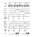
- the read signal RW and the reset signal RS are applied at a constant timing in each vertical period, and the reset signal RS in a certain vertical period with respect to the sensor circuit 81 in the n-th row. (N) is applied, and sensor circuit output data is read from the sensor circuit 81 by a read signal RW (n) applied in the next vertical period. That is, in the example of FIG. 12, the sensing period of the sensor circuit 81 has a length close to approximately one vertical period.
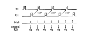
- the display device is characterized in that the output wiring SData is fixed to a predetermined potential V0 immediately before the read signal RW and the reset signal RS. For this reason, as shown in FIG. 13, the discharge signal DisC that is turned on immediately before the read signal RW and the reset signal RS is used as a control signal for applying the constant potential V0 to the output wiring SData.
- the potential V0 is arbitrary as long as it is a constant potential, and may be, for example, a ground potential.
- FIG. 14 an example of a circuit configuration for applying the discharge signal DisC to the output wiring SData is shown in FIG.
- the column driver 4 according to the present embodiment is characterized in that an analog switch 45 that is controlled to open and close by a discharge signal DisC is added to the basic configuration shown in FIGS. .
- One end of the analog switch 45 is connected to the constant voltage source V0, and the other end is connected to the output wiring SData.
- the potential of the output wiring SData is fixed to the constant potential V0 when the discharge signal DisC is ON, that is, immediately before the read signal RW and the reset signal RS. Therefore, as can be seen by comparing FIG. 15 with FIG. 30 referred to in the background art section, according to the configuration of the present embodiment, the influence of the potential fluctuation of the output wiring SData on the storage node via the parasitic capacitance is affected. Can be eliminated. Therefore, a highly accurate sensor circuit output from which the offset is removed can be obtained.
- the sensor circuit output data has an offset caused by the potential fluctuation of the output wiring SData immediately before the read signal RW and the reset signal RS even if the amount of light incident on the photodiode D1 is constant. Further, as described above, since this offset is not constant, it cannot be simply removed. However, also in this case, as described above, the potential of the output wiring SData is fixed to the constant potential V0 in synchronization with the discharge signal DisC that is turned on immediately before the read signal RW and the reset signal RS. It is possible to obtain a highly accurate sensor circuit output by removing the offset.
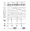
- the sensor circuit 81 is provided for each pixel in the row direction (vertical direction), and is driven at the timing shown in FIG. However, when the sensor circuit 81 is provided every other pixel in the row direction, the drive timing of the sensor circuit 81 is as shown in FIG. That is, the read signal RW and the reset signal RS are applied to the sensor circuit 81 every other horizontal period.
- the read signal RW is applied.
- the potential of the immediately preceding output wiring SData (Vw1, Vw2,... Shown in FIG. 30) depends on the immediately preceding display data. Further, the potential of the output wiring SData immediately before the reset signal RS is applied (Vs1, Vs2,... Shown in FIG. 30) also depends on the immediately preceding display data.
- the sensor circuit output data has an offset caused by the potential fluctuation of the output wiring SData immediately before the read signal RW and the reset signal RS even if the amount of light incident on the photodiode D1 is constant. Further, as described above, since this offset is not constant, it cannot be simply removed. However, also in this case, as described above, the potential of the output wiring SData is fixed to the constant potential V0 in synchronization with the discharge signal DisC that is turned on immediately before the read signal RW and the reset signal RS, so that the storage node and the output are output. An offset caused by the parasitic capacitance between the wiring SData and the wiring SData can be removed, and a highly accurate sensor circuit output can be obtained.
- the display device has the circuit configuration shown in FIG. 16, sensor circuits 81 are provided every other pixel in the row direction, and the sensor circuit 81 is driven at the timing shown in FIG. .
- the potential of the output wiring SData is fixed to the constant potential V0 immediately before the read signal RW and the reset signal RS.
- the difference from the first embodiment is as shown in FIG.
- the power supply voltage (VDD) that has been supplied to the sensor circuit 81 via the power supply line Vsup only when the read signal RW is applied is also supplied immediately before the reset signal RS.
- the display device includes an analog switch 44 that controls the supply of the power supply voltage (VDD) to the power supply line Vsup within the column driver 4, as shown in FIG. Opening and closing is performed by a signal VSW.
- the analog switch 44 of the power supply line Vsup is controlled to be opened and closed by the read signal RW.
- the potential of the power supply line Vsup to a predetermined potential (power supply voltage VDD) immediately before the reset signal RS by the signal VSW independent of the read signal RW, as shown in FIG.
- the potential of the power supply line Vsup immediately before the signal RW and the reset signal RS can be kept constant regardless of the previous state.
- the offset due to the parasitic capacitance between the storage node and the power supply line Vsup can be removed, and a highly accurate sensor circuit output can be obtained.
- the potential of the output wiring SData is fixed to the constant potential V0 immediately before the read signal RW and the reset signal RS, thereby causing the parasitic capacitance between the storage node and the output wiring SData. Therefore, it is possible to obtain a highly accurate sensor circuit output.
- the circuit configuration shown in FIG. 16 is provided, and the sensor circuit 81 is provided every other pixel in the row direction, and the sensor circuit 81 is installed at the timing shown in FIG.
- the case of driving was illustrated.
- the control of the power supply line Vsup by the signal VSW can be applied to the circuit configuration shown in FIG. 2 and has the same effect.
- the control of the power supply line Vsup by the signal VSW can be applied even when the sensor circuit 81 is driven at the timing shown in FIG. The same effect is produced.
- the display device has a circuit configuration shown in FIG. 16, and a sensor circuit 81 is provided in each pixel in the row direction, and drives the sensor circuit 81 at the timing shown in FIG.
- the potential of the output wiring SData is fixed to a predetermined potential immediately before the read signal RW and the reset signal RS.
- the predetermined potential is a predetermined level (Vx) input as a video signal, as shown in FIG.
- Vx a predetermined level
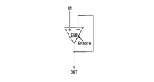
- the voltage follower output that constitutes the output amplifier circuit 33 (see FIG. 9 and the like) of the source driver 3 is used, and (2) the output amplifier circuit 33 of the source driver 3 is used.
- the output amplifier circuit 33 to the source line SL functioning as the wiring SData is, as shown in FIG. 21, a voltage follower circuit that applies negative feedback to the differential amplifier circuit. Realize. This circuit amplifies the current of the input voltage IN in the active state by the Enable output. On the other hand, in an inactive state, it becomes a high impedance state. Therefore, it is only necessary to turn on the enable signal also at the timing of the signal PCH shown in FIG.
- the output amplifier circuit 33 to the source line SL functioning as the wiring SData is provided with a switch in the differential amplifier circuit shown in FIG. 21, as shown in FIG.
- the configuration may be adopted.
- the constant voltage Vx can be output to the source line SL as the wiring SData only when the signal PCH is ON.
- the potential of the output wiring SData is fixed to the constant potential Vx immediately before the read signal RW and the reset signal RS, thereby causing the parasitic capacitance between the storage node and the output wiring SData. Therefore, it is possible to obtain a highly accurate sensor circuit output.
- the potential of the power supply line Vsup is fixed to a predetermined potential (power supply voltage VDD) immediately before the reset signal RS by the signal VSW independent of the read signal RW.
- VDD power supply voltage
- the potential of the power supply line Vsup immediately before the read signal RW and the reset signal RS can be kept constant regardless of the previous state.
- the offset due to the parasitic capacitance between the storage node and the power supply line Vsup can be removed, and a highly accurate sensor circuit output can be obtained.
- the circuit configuration shown in FIG. 16 is provided, and the sensor circuit 81 is provided every other pixel in the row direction, and the sensor circuit 81 is installed at the timing shown in FIG.
- the case of driving was illustrated.
- the sensor circuit 81 is provided for each pixel in the row direction, when the sensor circuit 81 is driven at the timing shown in FIG. 12, as described above, immediately before the readout signal RW and the reset signal RS.
- the potential of the output wiring SData By fixing the potential of the output wiring SData to the constant potential Vx, the same effect can be obtained.
- the display device has a circuit configuration shown in FIG. 16, and a sensor circuit 81 is provided in each pixel in the row direction, and drives the sensor circuit 81 at the timing shown in FIG. 12.
- a predetermined level (Vx) input as a video signal is input to the source line SL functioning as the wiring SData immediately before the read signal RW. (Refer to the third embodiment). Further, immediately before the reset signal RS, a predetermined voltage V0 is supplied to the source line SL functioning as the wiring SData (see the first embodiment).
- the potential of the power supply line Vsup is set to a predetermined potential immediately before the reset signal RS by the signal VSW independent of the read signal RW. It is fixed at (power supply voltage VDD) (see the second embodiment). Note that the voltages V0 and Vx are arbitrary on condition that they are constant values. Also, V0 and Vx may be different voltages.
- the offset caused by the parasitic capacitance between the storage node and the output wiring SData and the parasitic capacitance between the storage node and the power supply line Vsup are reduced. It is possible to remove both the resulting offset and obtain a highly accurate sensor circuit output.
- the potential of the wiring having parasitic capacitance with the storage node is fixed to a predetermined potential both before the read signal RW and immediately before the reset signal RS.
- the configuration in which the sensor circuit 81 includes the photodiode D1, the capacitor C2, and one thin film transistor M2 is exemplified.
- the present invention can also be applied to a configuration in which the sensor circuit 81 includes a photodiode D1, a capacitor C2, and three thin film transistors M2, M4, and M5.
- the sensor circuit 81 including the capacitor C2 is illustrated as the storage capacitor. However, even if the sensor circuit 81 does not have a circuit element corresponding to the storage capacitor, the sensor circuit 81 stores the capacitor C2. It is also possible to use a parasitic capacitance naturally generated in the node as a storage capacitor. Therefore, the capacitor C2 is not essential.
- the present invention is industrially applicable as a display device having an optical sensor in a pixel region of an active matrix substrate.
Abstract
Description
読み出し信号RWがハイレベルである期間が、読み出し期間に相当する。読み出し信号RWがハイレベルの間、コンデンサC2を介して蓄積ノードの電位VINTがプルアップされる。なお、蓄積ノードとは、コンデンサC2と、フォトダイオードD1のカソードと、トランジスタM2のゲートとの接続点である。このとき、蓄積ノードの電位VINTは、読出し直前の蓄積ノード電位をV0、コンデンサC2の容量をCst、回路内総容量をCtotal、読み出し信号RWの振幅をVrwとすると、
VINT = Cst/Ctotal・Vrw+V0
と表すことができる。
Vout ≒ VINT-Vth-(2I/β)1/2
と表すことができる。
リセット信号RSがハイレベル(0V)となることにより、フォトダイオードD1に順方向電流が流れ、蓄積ノードの電位VINTが0Vにリセットされる。
リセット信号がハイレベルからローレベルへ戻った時点から、センシング期間が開始される。すなわち、上述のとおりリセット期間に蓄積ノードがリセットされた後に、リセット信号RSがローレベル(-Vb)となることにより、フォトダイオードD1に逆バイアスが発生する。そして、フォトダイオードD1への入射光の光量に応じた光電流で、蓄積ノードが-Vb方向へ変化する。
図29に示した構成において、図30に示すように、リセット、センシング、読み出しを繰り返し行う場合、フォトダイオードD1へ入射する光量が一定であったとしても、出力配線SDataへ読み出されるセンサ回路出力データは、読み出し信号RWおよびリセット信号RSの直前の出力配線SDataの電位(図30に示すVs1,Vw2,Vs2,…)に影響され、変動する。なお、上記の出力配線SDataの電位Vs1,Vw2,Vs2,…は、その直前のセンサ回路出力データの電位に依存する。
また、読み出し信号RWのパルス3によって読み出されるセンサ回路出力データと、読み出し信号RWのパルス4によって読み出されるセンサ回路出力データとの間には、それぞれのセンシング期間にフォトダイオードD1へ入射する光量が同じであったとしても、寄生容量に起因して、以下のオフセットVoff3-4が生じる。
前述のように、出力配線SDataの電位Vs1,Vw2,Vs2,…は、その直前のセンサ回路出力データ(すなわち、同じ列で一つ前の行のセンサ回路からの出力データ)の電位に依存する。したがって、オフセットVoff2-3とオフセットVoff3-4とは、必ずしも一定ではない。以上のとおり、センサ回路出力データは、フォトダイオードD1へ入射する光量が一定であったとしても、読み出し信号RWおよびリセット信号RSの直前の出力配線SDataの電位変動から生じるオフセットを持つ。また、上述のとおり、このオフセットは一定ではないので、単純に除去することができない。
最初に、図1および図2を参照しながら、本発明の第1の実施形態にかかる液晶表示装置が備えるアクティブマトリクス基板の構成について説明する。
なお、本実施形態の上記の説明においては、図2に示したように、電源線Vsupおよびセンサ回路出力データの出力配線SDataがソース線SLとは別個に設けられた構成を例示した。しかし、図16に示すように、ソース線SLが電源線Vsupおよびセンサ回路出力データの出力配線SDataを兼ねている回路構成を採用しても良い。この構成において、かつ、図12に示したタイミングで駆動を行う場合においても、読み出し信号RWおよびリセット信号RSの直前に、出力配線SDataの電位を定電位V0に固定することにより、寄生容量に起因するオフセットを除去して精度の高いセンサ回路出力を得ることが可能となる。
また、本実施形態の上記の説明においては、センサ回路81が行方向(垂直方向)において1画素毎に設けられ、図12に示すようなタイミングで駆動を行うものとした。しかし、センサ回路81を行方向において1画素おきに設けた場合、センサ回路81の駆動タイミングは図17に示すとおりとなる。つまり、センサ回路81に対する読み出し信号RWおよびリセット信号RSの印加が1水平期間おきになる。
本発明の第2の実施形態について以下に説明する。なお、第1の実施形態において説明した構成と同様の機能を有する構成については、第1の実施形態と同じ参照符号を付記し、その詳細な説明を省略する。
本発明の第3の実施形態について以下に説明する。なお、前述の実施形態において説明した構成と同様の機能を有する構成については、それらの実施形態と同じ参照符号を付記し、その詳細な説明を省略する。
本発明の第4の実施形態について以下に説明する。なお、前述の実施形態において説明した構成と同様の機能を有する構成については、それらの実施形態と同じ参照符号を付記し、その詳細な説明を省略する。
Claims (7)
- アクティブマトリクス基板の画素領域に光センサを備えた表示装置であって、
前記光センサが、
入射光を受光する光検出素子と、
前記光検出素子に接続され、前記光検出素子からの出力電流によって電位が変化する蓄積ノードと、
当該光センサへリセット信号を供給するリセット信号配線と、
当該光センサへ読み出し信号を供給する読み出し信号配線と、
前記リセット信号が供給されてから前記読み出し信号が供給されるまでの間をセンシング期間とし、センシング期間に前記光検出素子で受光された光量にしたがって変化した前記蓄積ノードの電位をセンサ回路出力として出力配線へ読み出すためのセンサスイッチング素子とを備え、
前記読み出し信号の直前と、前記リセット信号の直前との少なくともいずれか一方において、前記蓄積ノードとの間で寄生容量を有する配線の電位を所定の電位に固定することを特徴とする表示装置。 - 前記蓄積ノードとの間で寄生容量を有する配線が、前記出力配線である、請求項1に記載の表示装置。
- 前記出力配線を前記所定の電位に固定するために、当該配線へ所定のレベルの映像信号を供給する、請求項2に記載の表示装置。
- 前記蓄積ノードとの間で寄生容量を有する配線が、前記読み出し信号が供給されている期間に前記光センサへ電源電圧を供給する電源配線であり、
前記電源配線は、前記画素領域の画素へ映像信号を供給するソース線を兼ねる、請求項1に記載の表示装置。 - 前記電源配線の前記所定の電位への固定を、前記読み出し信号とは異なる信号によって制御する、請求項4に記載の表示装置。
- 前記読み出し信号の直前に、前記出力配線を第1の所定の電位に固定するために、当該配線へ所定のレベルの映像信号を供給し、
前記リセット信号の直前に、前記出力配線を第2の所定の電位に固定するために、当該配線へ所定のレベルの電圧を供給する、請求項1に記載の表示装置。 - 前記アクティブマトリクス基板に対向する対向基板と、
前記アクティブマトリクス基板と対向基板との間に挟持された液晶とをさらに備えた、請求項1~6のいずれか一項に記載の表示装置。
Priority Applications (5)
| Application Number | Priority Date | Filing Date | Title |
|---|---|---|---|
| BRPI0918475A BRPI0918475A2 (pt) | 2008-09-02 | 2009-07-07 | dispositivo de display |
| US13/061,545 US8593443B2 (en) | 2008-09-02 | 2009-07-07 | Display device |
| CN2009801331475A CN102132233B (zh) | 2008-09-02 | 2009-07-07 | 显示装置 |
| JP2010527736A JP5258891B2 (ja) | 2008-09-02 | 2009-07-07 | 表示装置 |
| EP09811359.0A EP2323021A4 (en) | 2008-09-02 | 2009-07-07 | DISPLAY DEVICE |
Applications Claiming Priority (2)
| Application Number | Priority Date | Filing Date | Title |
|---|---|---|---|
| JP2008-224931 | 2008-09-02 | ||
| JP2008224931 | 2008-09-02 |
Publications (1)
| Publication Number | Publication Date |
|---|---|
| WO2010026830A1 true WO2010026830A1 (ja) | 2010-03-11 |
Family
ID=41797003
Family Applications (1)
| Application Number | Title | Priority Date | Filing Date |
|---|---|---|---|
| PCT/JP2009/062354 WO2010026830A1 (ja) | 2008-09-02 | 2009-07-07 | 表示装置 |
Country Status (7)
| Country | Link |
|---|---|
| US (1) | US8593443B2 (ja) |
| EP (1) | EP2323021A4 (ja) |
| JP (1) | JP5258891B2 (ja) |
| CN (1) | CN102132233B (ja) |
| BR (1) | BRPI0918475A2 (ja) |
| RU (1) | RU2449345C1 (ja) |
| WO (1) | WO2010026830A1 (ja) |
Cited By (4)
| Publication number | Priority date | Publication date | Assignee | Title |
|---|---|---|---|---|
| JP2011107761A (ja) * | 2009-11-12 | 2011-06-02 | Sony Corp | 撮像機能付き表示装置、駆動方法および電子機器 |
| JP2011210251A (ja) * | 2010-03-12 | 2011-10-20 | Semiconductor Energy Lab Co Ltd | 入力回路の駆動方法及び入出力装置の駆動方法 |
| JP2018075182A (ja) * | 2016-11-09 | 2018-05-17 | 株式会社日立製作所 | アナログ加算回路、それを用いた超音波探触子、および超音波診断装置 |
| US10685992B2 (en) | 2010-09-06 | 2020-06-16 | Semiconductor Energy Laboratory Co., Ltd. | Electronic device |
Families Citing this family (2)
| Publication number | Priority date | Publication date | Assignee | Title |
|---|---|---|---|---|
| CN113128318A (zh) | 2020-01-15 | 2021-07-16 | 群创光电股份有限公司 | 用于屏下生物表征辨识的电子装置 |
| TWI745081B (zh) * | 2020-09-14 | 2021-11-01 | 友達光電股份有限公司 | 光學觸控裝置 |
Citations (7)
| Publication number | Priority date | Publication date | Assignee | Title |
|---|---|---|---|---|
| JPH09247536A (ja) * | 1996-03-13 | 1997-09-19 | Toshiba Corp | Mos型固体撮像装置及びその駆動方法 |
| JPH1093066A (ja) * | 1996-09-17 | 1998-04-10 | Toshiba Corp | 固体撮像装置及びその駆動方法 |
| JPH11177886A (ja) * | 1997-12-15 | 1999-07-02 | Sharp Corp | 増幅型光電変換素子、増幅型固体撮像装置及びその駆動方法 |
| JP2004045879A (ja) * | 2002-07-12 | 2004-02-12 | Toshiba Matsushita Display Technology Co Ltd | 表示装置 |
| JP2006003857A (ja) | 2003-08-25 | 2006-01-05 | Toshiba Matsushita Display Technology Co Ltd | 表示装置および光電変換素子 |
| WO2007145347A1 (en) | 2006-06-12 | 2007-12-21 | Sharp Kabushiki Kaisha | Combined image sensor and display device |
| WO2007145346A1 (en) | 2006-06-12 | 2007-12-21 | Sharp Kabushiki Kaisha | Image sensor and display |
Family Cites Families (10)
| Publication number | Priority date | Publication date | Assignee | Title |
|---|---|---|---|---|
| JP4227770B2 (ja) * | 2002-07-10 | 2009-02-18 | シャープ株式会社 | 表示装置およびそれを備えた画像読み取り/表示システム |
| CN1331347C (zh) * | 2002-07-12 | 2007-08-08 | 东芝松下显示技术有限公司 | 显示装置 |
| US7295199B2 (en) * | 2003-08-25 | 2007-11-13 | Motorola Inc | Matrix display having addressable display elements and methods |
| KR100669270B1 (ko) * | 2003-08-25 | 2007-01-16 | 도시바 마쯔시따 디스플레이 테크놀로지 컴퍼니, 리미티드 | 표시 장치 및 광전 변환 소자 |
| JP4521176B2 (ja) * | 2003-10-31 | 2010-08-11 | 東芝モバイルディスプレイ株式会社 | 表示装置 |
| US8355015B2 (en) * | 2004-05-21 | 2013-01-15 | Semiconductor Energy Laboratory Co., Ltd. | Semiconductor device, display device and electronic device including a diode electrically connected to a signal line |
| JP4127243B2 (ja) * | 2004-05-24 | 2008-07-30 | セイコーエプソン株式会社 | 光センサ、光センサの読取方法、マトリクス型光センサ回路および電子機器 |
| JP4338140B2 (ja) | 2005-05-12 | 2009-10-07 | 株式会社 日立ディスプレイズ | タッチパネル一体表示装置 |
| RU2319991C1 (ru) | 2006-10-24 | 2008-03-20 | Самсунг Электроникс Ко., Лтд. | Жидкокристаллический дисплей |
| RU2451983C1 (ru) * | 2008-09-02 | 2012-05-27 | Шарп Кабусики Кайся | Дисплейное устройство |
-
2009
- 2009-07-07 EP EP09811359.0A patent/EP2323021A4/en not_active Withdrawn
- 2009-07-07 JP JP2010527736A patent/JP5258891B2/ja not_active Expired - Fee Related
- 2009-07-07 CN CN2009801331475A patent/CN102132233B/zh not_active Expired - Fee Related
- 2009-07-07 US US13/061,545 patent/US8593443B2/en not_active Expired - Fee Related
- 2009-07-07 WO PCT/JP2009/062354 patent/WO2010026830A1/ja active Application Filing
- 2009-07-07 RU RU2011112789/08A patent/RU2449345C1/ru not_active IP Right Cessation
- 2009-07-07 BR BRPI0918475A patent/BRPI0918475A2/pt not_active IP Right Cessation
Patent Citations (7)
| Publication number | Priority date | Publication date | Assignee | Title |
|---|---|---|---|---|
| JPH09247536A (ja) * | 1996-03-13 | 1997-09-19 | Toshiba Corp | Mos型固体撮像装置及びその駆動方法 |
| JPH1093066A (ja) * | 1996-09-17 | 1998-04-10 | Toshiba Corp | 固体撮像装置及びその駆動方法 |
| JPH11177886A (ja) * | 1997-12-15 | 1999-07-02 | Sharp Corp | 増幅型光電変換素子、増幅型固体撮像装置及びその駆動方法 |
| JP2004045879A (ja) * | 2002-07-12 | 2004-02-12 | Toshiba Matsushita Display Technology Co Ltd | 表示装置 |
| JP2006003857A (ja) | 2003-08-25 | 2006-01-05 | Toshiba Matsushita Display Technology Co Ltd | 表示装置および光電変換素子 |
| WO2007145347A1 (en) | 2006-06-12 | 2007-12-21 | Sharp Kabushiki Kaisha | Combined image sensor and display device |
| WO2007145346A1 (en) | 2006-06-12 | 2007-12-21 | Sharp Kabushiki Kaisha | Image sensor and display |
Non-Patent Citations (1)
| Title |
|---|
| See also references of EP2323021A4 |
Cited By (10)
| Publication number | Priority date | Publication date | Assignee | Title |
|---|---|---|---|---|
| JP2011107761A (ja) * | 2009-11-12 | 2011-06-02 | Sony Corp | 撮像機能付き表示装置、駆動方法および電子機器 |
| US8773415B2 (en) | 2009-11-12 | 2014-07-08 | Japan Display West Inc. | Display device with image pickup function, driving method, and electronic device |
| JP2011210251A (ja) * | 2010-03-12 | 2011-10-20 | Semiconductor Energy Lab Co Ltd | 入力回路の駆動方法及び入出力装置の駆動方法 |
| US9971440B2 (en) | 2010-03-12 | 2018-05-15 | Semiconductor Energy Laboratory Co., Ltd. | Method for driving circuit and method for driving display device |
| US10685992B2 (en) | 2010-09-06 | 2020-06-16 | Semiconductor Energy Laboratory Co., Ltd. | Electronic device |
| US11239268B2 (en) | 2010-09-06 | 2022-02-01 | Semiconductor Energy Laboratory Co., Ltd. | Electronic device |
| US11264415B2 (en) | 2010-09-06 | 2022-03-01 | Semiconductor Energy Laboratory Co., Ltd. | Electronic device |
| US11430820B2 (en) | 2010-09-06 | 2022-08-30 | Semiconductor Energy Laboratory Co., Ltd. | Electronic device |
| US11728354B2 (en) | 2010-09-06 | 2023-08-15 | Semiconductor Energy Laboratory Co., Ltd. | Electronic device |
| JP2018075182A (ja) * | 2016-11-09 | 2018-05-17 | 株式会社日立製作所 | アナログ加算回路、それを用いた超音波探触子、および超音波診断装置 |
Also Published As
| Publication number | Publication date |
|---|---|
| EP2323021A1 (en) | 2011-05-18 |
| US8593443B2 (en) | 2013-11-26 |
| JP5258891B2 (ja) | 2013-08-07 |
| US20110149174A1 (en) | 2011-06-23 |
| CN102132233B (zh) | 2013-11-13 |
| RU2449345C1 (ru) | 2012-04-27 |
| EP2323021A4 (en) | 2013-10-23 |
| JPWO2010026830A1 (ja) | 2012-02-02 |
| BRPI0918475A2 (pt) | 2015-12-01 |
| CN102132233A (zh) | 2011-07-20 |
Similar Documents
| Publication | Publication Date | Title |
|---|---|---|
| US10133384B2 (en) | Display device and method of driving the same | |
| JP5068320B2 (ja) | 表示装置 | |
| US8416225B2 (en) | Display device | |
| CN101680803B (zh) | 光传感器和包括该光传感器的显示装置 | |
| WO2009147914A1 (ja) | 表示装置 | |
| JP5258891B2 (ja) | 表示装置 | |
| JPWO2008047677A1 (ja) | 表示装置 | |
| US8525953B2 (en) | Display device | |
| WO2012008198A1 (ja) | 光センサ付き表示装置 | |
| US20100134452A1 (en) | Display device | |
| US20120112047A1 (en) | Sensor circuit and display apparatus | |
| WO2010007890A1 (ja) | 表示装置 | |
| WO2013084947A1 (ja) | 光センサ回路の動作方法、および、当該光センサ回路を備えた表示装置の動作方法 | |
| WO2010038513A1 (ja) | 表示装置 | |
| US9069412B2 (en) | Touch-sensor-equipped display device comrpising photodetecting elements | |
| WO2010001929A1 (ja) | 表示装置 | |
| JP5116851B2 (ja) | 表示装置 | |
| US20110102393A1 (en) | Display device | |
| US20130113768A1 (en) | Display device and drive method for same | |
| WO2012014861A1 (ja) | 表示装置 | |
| WO2010100785A1 (ja) | 表示装置 | |
| TWI756098B (zh) | 指紋畫素單元、指紋感測裝置及整合積體電路 | |
| KR20050121380A (ko) | 표시 장치 |
Legal Events
| Date | Code | Title | Description |
|---|---|---|---|
| WWE | Wipo information: entry into national phase |
Ref document number: 200980133147.5 Country of ref document: CN |
|
| 121 | Ep: the epo has been informed by wipo that ep was designated in this application |
Ref document number: 09811359 Country of ref document: EP Kind code of ref document: A1 |
|
| WWE | Wipo information: entry into national phase |
Ref document number: 2010527736 Country of ref document: JP |
|
| WWE | Wipo information: entry into national phase |
Ref document number: 2009811359 Country of ref document: EP |
|
| WWE | Wipo information: entry into national phase |
Ref document number: 13061545 Country of ref document: US |
|
| WWE | Wipo information: entry into national phase |
Ref document number: 1466/CHENP/2011 Country of ref document: IN |
|
| NENP | Non-entry into the national phase |
Ref country code: DE |
|
| WWE | Wipo information: entry into national phase |
Ref document number: 2011112789 Country of ref document: RU |
|
| ENP | Entry into the national phase |
Ref document number: PI0918475 Country of ref document: BR Kind code of ref document: A2 Effective date: 20110301 |