WO2010026641A1 - 試験装置および試験方法 - Google Patents
試験装置および試験方法 Download PDFInfo
- Publication number
- WO2010026641A1 WO2010026641A1 PCT/JP2008/066004 JP2008066004W WO2010026641A1 WO 2010026641 A1 WO2010026641 A1 WO 2010026641A1 JP 2008066004 W JP2008066004 W JP 2008066004W WO 2010026641 A1 WO2010026641 A1 WO 2010026641A1
- Authority
- WO
- WIPO (PCT)
- Prior art keywords
- test
- detection
- unit
- execution
- value
- Prior art date
- Legal status (The legal status is an assumption and is not a legal conclusion. Google has not performed a legal analysis and makes no representation as to the accuracy of the status listed.)
- Ceased
Links
Images




Classifications
-
- G—PHYSICS
- G11—INFORMATION STORAGE
- G11C—STATIC STORES
- G11C29/00—Checking stores for correct operation ; Subsequent repair; Testing stores during standby or offline operation
- G11C29/56—External testing equipment for static stores, e.g. automatic test equipment [ATE]; Interfaces therefor
-
- G—PHYSICS
- G01—MEASURING; TESTING
- G01R—MEASURING ELECTRIC VARIABLES; MEASURING MAGNETIC VARIABLES
- G01R31/00—Arrangements for testing electric properties; Arrangements for locating electric faults; Arrangements for electrical testing characterised by what is being tested not provided for elsewhere
- G01R31/28—Testing of electronic circuits, e.g. by signal tracer
-
- G—PHYSICS
- G11—INFORMATION STORAGE
- G11C—STATIC STORES
- G11C16/00—Erasable programmable read-only memories
- G11C16/02—Erasable programmable read-only memories electrically programmable
- G11C16/04—Erasable programmable read-only memories electrically programmable using variable threshold transistors, e.g. FAMOS
Definitions
- the present invention relates to a test apparatus and a test method for testing a device under test.
- a test apparatus for testing a device under test such as a semiconductor supplies a test signal having a predetermined test pattern to the device under test, and detects a value of a signal output from the device under test according to the test signal. Then, the test apparatus determines the quality of the device under test by comparing the detected signal value with the expected value.
- Such a test apparatus includes a pattern generator.
- the pattern generator sequentially executes each test instruction included in the test instruction sequence (sequence data).
- the pattern generator sequentially outputs test patterns corresponding to the executed test instructions.
- the pattern generator can execute a test instruction called a match instruction (see Patent Document 1 and Patent Document 2).
- the match instruction detects whether or not the value of the output signal of the device under test matches the expected value, and the command differs depending on whether the output signal value matches the expected value or not.
- a branch instruction that branches.
- test apparatus By executing a test instruction sequence including such a match instruction, the test apparatus can perform the following operation, for example.
- a device under test having a PLL Phase Locked Loop outputs a lock signal when the PLL is stable.
- PLL Phase Locked Loop
- Such a test apparatus for testing a device under test uses a match instruction to execute processing for exiting the loop on condition that the value of the lock signal matches a predetermined value. As a result, the test apparatus can execute the original function test after the PLL operates stably after the power is turned on.
- the NAND flash memory outputs a ready / busy signal indicating whether or not an erasing operation (or recording operation) is in progress.
- a test apparatus for testing such a NAND flash memory detects that the value of the ready / busy signal matches the expected value by a match instruction when the NAND flash memory is erased or recorded. Later, the next test is performed. Accordingly, the test apparatus can execute the next test after the erase operation or the recording operation in the NAND flash memory is completed with certainty.
- the test apparatus when executing the match instruction, the test apparatus must previously assign hardware that detects whether or not the value of the output signal matches the expected value to a terminal to be detected by the match instruction. Therefore, the test apparatus cannot dynamically change the terminal to be detected by the match instruction during the execution of the test sequence.
- the test apparatus when testing a device under test that represents three or more states based on a plurality of output signal values, the test apparatus is required to branch to a different instruction for each of the three or more states.
- the test apparatus cannot dynamically change the terminal that is the target of detection of the match instruction during the execution of the test sequence, and has three or more states represented by a plurality of output signals. Since it is very difficult to detect by hardware, it is not possible to shift to a different instruction for each of the three or more states.
- an object of the present invention is to provide a test apparatus and a test method that can solve the above-described problems. This object is achieved by a combination of features described in the independent claims.
- the dependent claims define further advantageous specific examples of the present invention.
- a test apparatus for testing a device under test having a plurality of output terminals, wherein a test instruction sequence for testing the device under test is executed.
- a storage unit that stores a plurality of setting data that specifies at least one output terminal among the plurality of output terminals, and an output signal value from the output terminal that is specified by the setting data is an expected value.
- different setting data in the storage section are selected.
- a selection unit that supplies the detection unit, and a test method related to the test device.
- FIG. 1 shows a configuration of a test apparatus 10 according to an embodiment of the present invention, together with a device under test 300.
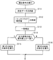
- FIG. 2 shows a processing flow when the detection command is executed in the test apparatus 10 according to the embodiment of the present invention.
- FIG. 3 shows an example of the configuration of the storage unit 34, the selection unit 36, and the detection unit 38.
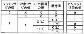
- FIG. 4 shows the relationship between the signal input to the terminal correspondence detection unit 46 and the signal output from the terminal correspondence detection unit 46.
- FIG. 5 is a flowchart showing an example of a sequence executed by the execution unit 20. An example of the object flag memorize
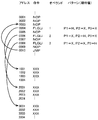
- FIG. 7 shows an example of a test instruction sequence for causing the sequence shown in FIG. 5 to be executed.
- FIG. 1 shows a configuration of a test apparatus 10 according to this embodiment together with a device under test 300.
- the test apparatus 10 tests a device under test 300 having a plurality of output terminals.
- the test apparatus 10 includes a main body 12 and a control device 14.
- the main body section 12 exchanges signals with the device under test 300.
- the control apparatus 14 executes a control program for controlling the test of the device under test 300 by the test apparatus 10 and controls the operation of the main body unit 12.
- the main body 12 includes an execution unit 20, a signal supply unit 30, a comparison unit 32, a storage unit 34, a selection unit 36, and a detection unit 38.
- the execution unit 20 executes a test instruction sequence for testing the device under test 300. More specifically, the execution unit 20 sequentially executes each test instruction included in the test instruction sequence. Then, the execution unit 20 generates a pattern (test pattern and expected value pattern) stored in association with the executed test instruction. Thus, the execution unit 20 can generate a test pattern indicating a pattern of a test signal to be given to the device under test 300 and an expected value of the output signal to be output from the device under test 300. The execution unit 20 receives the test instruction sequence from the control device 14 prior to execution of the test instruction sequence.
- the signal supply unit 30 generates a test signal having a waveform corresponding to the test pattern generated by the execution unit 20 and supplies it to the device under test 300. As a result, the device under test 300 operates in accordance with the given test signal.
- the comparison unit 32 receives an output signal output from the device under test 300 according to the given test signal. Then, the comparison unit 32 compares the value of the received output signal with the expected value generated by the execution unit 20, and outputs a comparison result.
- the storage unit 34 stores a plurality of setting data for designating at least one output terminal among a plurality of output terminals that output an output signal in the device under test 300.
- the storage unit 34 stores a plurality of setting data each having unique identification information. Further, the storage unit 34 receives and stores a plurality of setting data from the control device 14 prior to execution of the test instruction sequence by the execution unit 20.
- the selection unit 36 selects setting data designated by the execution unit 20 from among a plurality of setting data stored in the storage unit 34 and supplies the selected setting data to the detection unit 38.
- the selection unit 36 receives identification information included in a detection command executed by the execution unit 20 (details of the detection command will be described later), and selects setting data corresponding to the received identification information from the storage unit 34. Then, it is given to the detection unit 38.
- the detection unit 38 detects whether or not the value of the output signal from the output terminal specified by the given setting data matches the expected value generated by the execution unit 20. Then, the detection unit 38 gives the detection result to the execution unit 20.
- FIG. 2 shows a processing flow when the detection command is executed in the test apparatus 10 according to the present embodiment.
- the control device 14 Prior to the execution of the test instruction sequence by the execution unit 20, the control device 14 writes the test instruction sequence described in the test program, for example, in the execution unit 20. Further, prior to the execution of the test instruction sequence by the execution unit 20, the control device 14 writes the value of the setting data described in the control program, for example, in the storage unit 34.
- the execution unit 20 sequentially executes each test instruction included in the test instruction sequence, for example, from the test instruction at the head address.
- the test command sequence executed by the execution unit 20 may include a detection command.
- the detection command is a command for changing the execution sequence of the test command sequence according to the detection result by the detection unit 38. That is, the detection command causes the detection unit 38 to detect whether the value of the output signal of the device under test 300 matches the expected value, and jumps to the next command to be executed according to the detection result by the detection unit 38. It is an instruction to switch the destination. For example, the detection instruction branches to an instruction ahead of the detection instruction on condition that the value of the output signal does not match the expected value, and on the condition that the value of the output signal matches the expected value. It may be an instruction that branches to an instruction at a rear address (for example, the next address). Thus, the detection instruction can execute a loop process that repeats the loop until the value of the output signal matches the expected value.
- the detection command includes information for designating one setting data to be supplied to the detection unit 38 from among a plurality of setting data stored in the storage unit 34.
- the detection command includes identification information of setting data to be supplied to the detection unit 38 as an operand.
- the test apparatus 10 executes the processing flow shown in FIG.
- the selection unit 36 selects one setting data designated by the detection command from a plurality of setting data stored in advance in the storage unit 34 and supplies the selected setting data to the selection unit 36. (S111).
- the selection unit 36 receives the identification information included in the operand of the detection instruction from the execution unit 20, selects setting data corresponding to the received identification information from the storage unit 34, and supplies the setting data to the detection unit 38. To do. Thereby, the selection unit 36 can select different setting data in the storage unit 34 and supply the selected setting data to the detection unit 38 in the execution of at least two detection commands.
- the identification information may be included in a part of the pattern associated with the detection instruction.
- the execution unit 20 extracts the identification information from a part of the pattern associated with the detection instruction and supplies the identification information to the selection unit 36.
- the execution unit 20 supplies a match flag indicating execution of the detection command and an expected value of the output signal to be detected to the detection unit 38 (S112).
- the detection unit 38 uses the value of the output signal of the output terminal specified by the given setting data on the condition that the match flag is given (for example, on the condition that the value of the match flag becomes "1"). And whether or not the corresponding expected values all match (S113).
- the execution unit 20 follows the detection command and executes the detection command.
- the test instruction of the first branch destination designated by (1) is executed (S115).
- the execution unit 20 follows the detection command.
- the test instruction of the second branch destination different from the first branch destination designated by the detection instruction is executed (S116).
- the selection unit 36 selects one setting data from the plurality of setting data stored in advance by the storage unit 34 and supplies the selected setting data to the detection unit 38. Then, the detection unit 38 detects whether or not the output signal output from the output terminal specified by the given setting data matches the expected value. Thereby, the test apparatus 10 can change the output terminal used as the object which detects whether it corresponds with an expected value for every execution of each detection command.
- FIG. 3 shows an example of the configuration of the storage unit 34, the selection unit 36, and the detection unit 38.
- FIG. 4 shows the relationship between the signal input to the terminal correspondence detection unit 46 and the signal output from the terminal correspondence detection unit 46.
- the storage unit 34 may include a plurality of terminal correspondence storage units 42.
- the selection unit 36 may include a plurality of terminal correspondence selection units 44.
- the detection unit 38 may include a plurality of terminal correspondence detection units 46, an overall match detection unit 48, and a plurality of target terminal setting units 50.
- Each of the plurality of terminal correspondence storage units 42 is provided corresponding to each of the plurality of output terminals of the device under test 300.
- Each terminal correspondence storage unit 42 stores a target flag indicating whether or not the corresponding output terminal is a detection target by the detection unit 38 for each value of the identification information.
- each terminal correspondence storage unit 42 is written with a target flag indicating “1” when it is a detection target and “0” when it is not a detection target.
- Each of the plurality of terminal correspondence selecting units 44 is provided corresponding to each of the plurality of output terminals of the device under test 300.
- Each terminal correspondence selection unit 44 receives the value of the identification information included in the detection command from the execution unit 20 when the execution unit 20 executes the detection command. Then, each terminal correspondence selecting unit 44 selects a target flag corresponding to the value of the received identification information stored in the corresponding terminal correspondence storing unit 42, and corresponding terminal correspondence detecting unit 46 in the detecting unit 38. To give.
- Each of the plurality of terminal correspondence detection units 46 is provided corresponding to each of the plurality of output terminals of the device under test 300.
- Each terminal correspondence detection unit 46 receives the match flag from the execution unit 20. Furthermore, each terminal correspondence detection unit 46 receives an output signal from a corresponding output terminal of the device under test 300, receives an expected value of an output signal output from the corresponding output terminal from the execution unit 20, and selects a corresponding terminal correspondence.
- a target flag is received from the unit 44.
- each of the plurality of terminal correspondence detection units 46 Based on these signals, each of the plurality of terminal correspondence detection units 46 outputs a pin match signal indicating that the output signal from the output terminal matches the expected value. More specifically, each terminal correspondence detection unit 46 is supplied with a match flag, and a target flag indicating that the corresponding output terminal is a detection target is supplied from the corresponding terminal correspondence storage unit 42, and the output A pin match signal is output on condition that the value of the output signal from the terminal matches the expected value. Alternatively, each terminal correspondence detection unit 46 is provided with a pin match signal provided that a match flag is supplied and a target flag indicating that the corresponding output terminal is not a detection target is supplied from the corresponding terminal correspondence storage unit 42. Is output.
- compatible detection part 46 does not output a pin match signal, when the match flag is not supplied.
- each terminal correspondence detection unit 46 performs pin matching when the value of the output signal from the corresponding output terminal does not match the expected value even when the match flag is supplied and the target flag is supplied. No signal is output.
- each terminal correspondence detection unit 46 outputs a pin match signal as shown in FIG. That is, each terminal correspondence detection unit 46 sets the value of the pin match signal to “0” regardless of the value of the target flag, the value of the output signal, and the expected value when the value of the match flag is “0”. Each terminal correspondence detection unit 46 sets the value of the pin match signal to “1” regardless of the value of the output signal and the expected value when the value of the match flag is “1” and the value of the target flag is “0”. To do.
- each terminal correspondence detection unit 46 when the value of the match flag is “1” and the value of the target flag is “1”, sets the output of the pin match signal on the condition that the value of the output signal matches the expected value. The value is “1”. In addition, each terminal correspondence detection unit 46, when the value of the match flag is “1” and the value of the target flag is “1”, sets the pin match signal as long as the output signal value does not match the expected value. The value is set to “0”.
- each of the plurality of terminal correspondence detection units 46 may further receive a mask signal indicating that the corresponding output terminal is not a subject of the test.
- each terminal correspondence detection unit 46 receives a value written in a predetermined register or the like by the control device 14 as a mask signal.
- Each terminal correspondence detection unit 46 outputs a pin match signal regardless of the match flag, the value of the output signal, the expected value, and the target flag on condition that the mask signal is given.
- the control device 14 can set, for example, the terminal correspondence detection unit 46 not connected to the device under test 300 so as to output a pin match signal regardless of the target flag or the like.
- the overall match detection unit 48 outputs an overall match signal indicating that the output signal from the output terminal to be detected matches the expected value in response to the pin match signal output from all the terminal correspondence detection units 46. Output to the execution unit 20.
- the overall match detection unit 48 outputs the overall match signal indicating “1”. Output to the execution unit 20.
- the overall match detection unit 48 indicates the overall match indicating “0” on condition that the pin match signal output from each of the plurality of terminal correspondence detection units 46 includes a pin match signal having a value of “0”. The signal is output to the execution unit 20. Then, the execution unit 20 that has received such an overall match signal changes the test instruction execution sequence in accordance with the value of the overall match signal.
- Each of the plurality of target terminal setting units 50 receives a terminal setting signal indicating whether or not the corresponding output terminal is to be detected by the detection command.
- each target terminal setting unit 50 receives a value written by the control device 14 in a predetermined register or the like as a terminal setting signal.
- Each target terminal setting unit 50 supplies the target flag to the corresponding terminal correspondence detecting unit 46 on condition that the terminal setting signal is given. Further, each target terminal setting unit 50 does not supply the target flag to the terminal correspondence detection unit 46 on condition that no terminal setting signal is given (for example, the value of the target flag is fixed to 0).
- control device 14 uses the list of output terminals that can be detected described in the control program to correspond to the output terminals that are not to be detected.
- the correspondence detection unit 46 can be set to output a pin match signal regardless of the value of the target flag.
- the storage unit 34 and the selection unit 36 configured as described above select and detect one setting data from a plurality of setting data stored in advance by the storage unit 34.
- the portion 38 can be supplied.
- the detection part 38 of such a structure can detect whether the output signal output from the output terminal designated with the given setting data and an expected value correspond.
- the control device 14 Prior to the execution of the test instruction sequence by the execution unit 20, the control device 14 detects the output terminals corresponding to the terminal correspondence storage units 42 of all the output terminals corresponding to the value of at least one identification information. It is also possible to write a target flag indicating that For example, the control device 14 writes a target flag of a value (in this example, “1”) for which the output terminal is a detection target, corresponding to the identification information at the head of each of the plurality of terminal correspondence storage units 42. It's okay.
- the detection unit 38 matches the expected value of the output signal only for the terminal to which the terminal setting signal is given. It is possible to detect whether or not. That is, the detection unit 38 can detect whether the value of the output signal matches the expected value for the output terminal specified by the control device 14 prior to execution of the test instruction sequence.
- FIG. 5 is a flowchart showing an example of a sequence executed by the execution unit 20.
- 6A, FIG. 6B, and FIG. 6C show an example of the target flag stored in the terminal correspondence storage unit 42 for causing the sequence shown in FIG. 5 to be executed.
- FIG. 7 shows an example of a test instruction sequence for causing the sequence shown in FIG. 5 to be executed.
- the execution unit 20 executes the sequence shown in the flow of FIG.
- the first output terminal is H logic (Yes in S121)
- the process jumps to the first branch destination (S122), and when the second output terminal is H logic (Yes in S123). ), Jump to the second branch destination (S124).
- the third output terminal is H logic (Yes in S125)
- the process waits in the loop.
- the control device 14 When executing such a sequence, the control device 14 prior to the execution of the test instruction sequence by the execution unit 20, the target flag as shown in FIG. 6A, for example, in the terminal correspondence storage unit 42 corresponding to the first output terminal. Write. That is, the control device 14 writes a target flag having a value 1 in the identification information 1 and a value 0 in the identification information 2 and 3.
- the control device 14 writes a target flag such as shown in FIG. 6B in the terminal correspondence storage unit 42 corresponding to the second output terminal. That is, the control device 14 writes a target flag having a value 1 in the identification information 2 and a value 0 in the identification information 1 and 3.
- the control device 14 writes a target flag as shown in FIG. 6B, for example, in the terminal correspondence storage unit 42 corresponding to the third output terminal. That is, the control device 14 writes a target flag having a value 1 in the identification information 3 and a value 0 in the identification information 1 and 2.
- the control device 14 causes the execution unit 20 to execute a test instruction sequence as shown in FIG.
- the NOP instruction is an instruction that shifts the process to the instruction at the next address.
- the JMP instruction is an instruction that jumps forward to an instruction at a specified address.
- the FLGLi instruction is an example of a detection instruction. More specifically, the FLGLi instruction includes identification information in the operand, and causes the detection unit 38 to detect whether the value of the output signal of the output terminal specified by the identification information matches the expected value. If the FLGLi instruction matches, the process jumps to the designated address i. If the FLGLi instruction does not match, the process shifts to the instruction at the next address.
- the test instruction sequence shown in FIG. 7 includes a first FLGLi instruction (address 0004), a second FLGLi instruction (address 0006), and a third one in a loop (address 0003 to 0010) formed in the JMP instruction.
- FLGLi instruction (address 0008) is arranged.
- the first FLGLi instruction detects whether or not the value of the first output terminal (P1) matches H logic, and if it matches, jumps to address 1001 and exits the loop.
- the second FLGLi instruction (address 0006) detects whether or not the value of the second output terminal (P2) matches H logic, and if it matches, jumps to address 2001 and exits the loop.
- the third FLGLi instruction (address 0008) detects whether or not the value of the third output terminal (P3) matches H logic, and if it matches, jumps to address 3001 and exits the loop.
- the test apparatus 10 can dynamically change the output terminal for detecting such a match / mismatch during the test sequence. As a result, the test apparatus 10 can jump to a different instruction in the test instruction sequence for each of the three or more states represented by the plurality of output signals of the device under test 300.
Landscapes
- Engineering & Computer Science (AREA)
- Microelectronics & Electronic Packaging (AREA)
- General Engineering & Computer Science (AREA)
- Physics & Mathematics (AREA)
- General Physics & Mathematics (AREA)
- Tests Of Electronic Circuits (AREA)
Abstract
Description
Claims (8)
- 複数の出力端子を備える被試験デバイスを試験する試験装置であって、
前記被試験デバイスを試験するための試験命令列を実行する実行部と、
前記複数の出力端子のうち少なくとも1つの出力端子を指定する複数の設定データを記憶する記憶部と、
前記設定データにより指定される出力端子からの出力信号の値が期待値と一致するか否かを検出する検出部と、
前記検出部による検出結果に応じて前記試験命令列の実行シーケンスを変更する少なくとも2つの検出命令の実行において、前記記憶部内の異なる設定データを選択して前記検出部に供給する選択部と、
を備える試験装置。 - 前記実行部は、前記検出部に供給すべき前記設定データの識別情報をオペランドとして含む前記検出命令を実行し、
前記選択部は、それぞれの前記検出命令の実行において、前記検出命令に含まれる前記識別情報に対応する前記設定データを前記記憶部から選択して前記検出部に供給する請求項1に記載の試験装置。 - 前記記憶部は、前記複数の出力端子のそれぞれに対応して、対応する前記出力端子を前記検出部による検出対象とするか否かを示す対象フラグを前記識別情報の値毎に記憶する端子対応記憶部を有する請求項2に記載の試験装置。
- 前記検出部は、
前記複数の出力端子のそれぞれに対応して設けられ、対応する前記出力端子が検出対象でないことを示す対象フラグが対応する前記端子対応記憶部から供給されたこと、または、対応する前記出力端子が検出対象であることを示す対象フラグが対応する前記端子対応記憶部から供給され、かつ、当該出力端子からの出力信号の値が期待値と一致したことを条件として、当該出力端子からの出力信号が期待値と一致したことを示すピンマッチ信号を出力する端子対応検出部と、
全ての前記端子対応検出部からピンマッチ信号が出力されたことに応じて、検出対象とする出力端子からの出力信号が期待値と一致したことを示す全体マッチ信号を出力する全体マッチ検出部と、
を有し、
前記実行部は、前記全体マッチ信号の値に応じて前記試験命令列の実行シーケンスを変更する
請求項3に記載の試験装置。 - 当該試験装置による前記被試験デバイスの試験を制御する制御プログラムを実行する制御装置を更に備え、
前記制御装置は、前記実行部による前記試験命令列の実行に先立って、前記制御プログラム中に記述された前記設定データの値を前記記憶部に書き込む
請求項4に記載の試験装置。 - 前記実行部による前記試験命令列の実行に先立って、前記制御装置は、前記制御プログラム中に記述された検出対象となりうる前記出力端子のリストに基づいて、検出対象とならない前記出力端子に対応する前記端子対応検出部を、対象フラグの値に関わらずピンマッチ信号を出力するように設定する請求項5に記載の試験装置。
- 前記実行部による前記試験命令列の実行に先立って、前記制御装置は、少なくとも1つの前記識別情報の値に対応して、全ての前記出力端子の前記端子対応記憶部に対応する前記出力端子を検出対象とする旨を示す対象フラグを書き込む請求項5から6のいずれかに記載の試験装置。
- 複数の出力端子を備える被試験デバイスを試験する試験装置により実行される試験方法であって、
前記試験装置は、
前記被試験デバイスを試験するための試験命令列を実行する実行部と、
前記複数の出力端子のうち少なくとも1つの出力端子を指定する複数の設定データを記憶する記憶部と、
前記設定データにより指定される出力端子からの出力信号の値が期待値と一致するか否かを検出する検出部とを備え、
前記検出部による検出結果に応じて前記試験命令列の実行シーケンスを変更する少なくとも2つの検出命令の実行において、前記記憶部内の異なる設定データを選択して前記検出部に供給する
試験方法。
Priority Applications (4)
| Application Number | Priority Date | Filing Date | Title |
|---|---|---|---|
| JP2010527625A JP5153880B2 (ja) | 2008-09-04 | 2008-09-04 | 試験装置および試験方法 |
| KR1020117003479A KR101213164B1 (ko) | 2008-09-04 | 2008-09-04 | 시험 장치 및 시험 방법 |
| PCT/JP2008/066004 WO2010026641A1 (ja) | 2008-09-04 | 2008-09-04 | 試験装置および試験方法 |
| US13/026,160 US8880375B2 (en) | 2008-09-04 | 2011-02-11 | Test apparatus and test method |
Applications Claiming Priority (1)
| Application Number | Priority Date | Filing Date | Title |
|---|---|---|---|
| PCT/JP2008/066004 WO2010026641A1 (ja) | 2008-09-04 | 2008-09-04 | 試験装置および試験方法 |
Related Child Applications (1)
| Application Number | Title | Priority Date | Filing Date |
|---|---|---|---|
| US13/026,160 Continuation US8880375B2 (en) | 2008-09-04 | 2011-02-11 | Test apparatus and test method |
Publications (1)
| Publication Number | Publication Date |
|---|---|
| WO2010026641A1 true WO2010026641A1 (ja) | 2010-03-11 |
Family
ID=41796829
Family Applications (1)
| Application Number | Title | Priority Date | Filing Date |
|---|---|---|---|
| PCT/JP2008/066004 Ceased WO2010026641A1 (ja) | 2008-09-04 | 2008-09-04 | 試験装置および試験方法 |
Country Status (4)
| Country | Link |
|---|---|
| US (1) | US8880375B2 (ja) |
| JP (1) | JP5153880B2 (ja) |
| KR (1) | KR101213164B1 (ja) |
| WO (1) | WO2010026641A1 (ja) |
Cited By (2)
| Publication number | Priority date | Publication date | Assignee | Title |
|---|---|---|---|---|
| JP2012104204A (ja) * | 2010-11-11 | 2012-05-31 | Advantest Corp | 試験装置 |
| CN114035781A (zh) * | 2021-11-12 | 2022-02-11 | 东软集团股份有限公司 | 测试脚本的处理方法、装置、存储介质和电子设备 |
Citations (1)
| Publication number | Priority date | Publication date | Assignee | Title |
|---|---|---|---|---|
| WO2004070404A1 (ja) * | 2003-02-04 | 2004-08-19 | Advantest Corporation | 試験装置 |
Family Cites Families (9)
| Publication number | Priority date | Publication date | Assignee | Title |
|---|---|---|---|---|
| TW382657B (en) | 1997-06-13 | 2000-02-21 | Advantest Corp | Memory tester |
| JPH1164454A (ja) | 1997-08-18 | 1999-03-05 | Advantest Corp | 半導体試験装置用同時測定制御回路 |
| JP4156712B2 (ja) | 1998-07-24 | 2008-09-24 | 株式会社アドバンテスト | 半導体試験装置の試験方法 |
| JP4130801B2 (ja) * | 2001-06-13 | 2008-08-06 | 株式会社アドバンテスト | 半導体デバイス試験装置、及び半導体デバイス試験方法 |
| KR100856608B1 (ko) | 2004-06-17 | 2008-09-03 | 주식회사 아도반테스토 | 시험 장치 및 시험 방법 |
| JP4279751B2 (ja) * | 2004-08-23 | 2009-06-17 | 株式会社アドバンテスト | デバイスの試験装置及び試験方法 |
| US7213182B2 (en) * | 2005-01-19 | 2007-05-01 | Advantest Corporation | Test apparatus and test method |
| US7574633B2 (en) * | 2006-07-12 | 2009-08-11 | Advantest Corporation | Test apparatus, adjustment method and recording medium |
| US7774669B2 (en) * | 2007-06-11 | 2010-08-10 | Lsi Corporation | Complex pattern generator for analysis of high speed serial streams |
-
2008
- 2008-09-04 KR KR1020117003479A patent/KR101213164B1/ko active Active
- 2008-09-04 WO PCT/JP2008/066004 patent/WO2010026641A1/ja not_active Ceased
- 2008-09-04 JP JP2010527625A patent/JP5153880B2/ja not_active Expired - Fee Related
-
2011
- 2011-02-11 US US13/026,160 patent/US8880375B2/en active Active
Patent Citations (1)
| Publication number | Priority date | Publication date | Assignee | Title |
|---|---|---|---|---|
| WO2004070404A1 (ja) * | 2003-02-04 | 2004-08-19 | Advantest Corporation | 試験装置 |
Cited By (2)
| Publication number | Priority date | Publication date | Assignee | Title |
|---|---|---|---|---|
| JP2012104204A (ja) * | 2010-11-11 | 2012-05-31 | Advantest Corp | 試験装置 |
| CN114035781A (zh) * | 2021-11-12 | 2022-02-11 | 东软集团股份有限公司 | 测试脚本的处理方法、装置、存储介质和电子设备 |
Also Published As
| Publication number | Publication date |
|---|---|
| US20110196640A1 (en) | 2011-08-11 |
| JP5153880B2 (ja) | 2013-02-27 |
| KR20110039350A (ko) | 2011-04-15 |
| JPWO2010026641A1 (ja) | 2012-01-26 |
| US8880375B2 (en) | 2014-11-04 |
| KR101213164B1 (ko) | 2012-12-24 |
Similar Documents
| Publication | Publication Date | Title |
|---|---|---|
| JP6267513B2 (ja) | 同一のデータ条件に依存する、隣接する命令の実行の制御 | |
| US8429380B2 (en) | Disabling redundant subfunctional units receiving same input value and outputting same output value for the disabled units in SIMD processor | |
| US8418011B2 (en) | Test module and test method | |
| US7359822B2 (en) | Testing device | |
| JP5153880B2 (ja) | 試験装置および試験方法 | |
| CN1761940B (zh) | 指令处理设备,指令执行方法和装置,指令编译方法和装置 | |
| CN111045880A (zh) | 芯片测试方法、验证系统及存储介质 | |
| JP5304239B2 (ja) | プロセッサ試験装置、プロセッサ試験方法、プロセッサ試験プログラム | |
| JP4568055B2 (ja) | 試験装置及び試験方法 | |
| KR100277770B1 (ko) | 시퀀스 제어회로 | |
| CN116129985B (zh) | 一种内存测试装置和内存测试方法 | |
| JP2005249735A (ja) | パターン発生器、及び試験装置 | |
| KR100790470B1 (ko) | 디바이스 드라이버 테스트를 위한 테스트 케이스 자동 생성방법 및 장치 | |
| KR20060019609A (ko) | 시험 장치, 및 프로그램 | |
| JP2006030090A (ja) | 試験装置及び試験方法 | |
| JP2006221624A (ja) | Vliwアーキテクチャを拡張させるデータ処理ユニットの効率的及び柔軟性のあるシーケンス動作のための方法及び装置 | |
| JP2673602B2 (ja) | 制御装置 | |
| EP3998532B1 (en) | Method for the selective tracing of the execution of instructions, related processing device and processor | |
| JP2009075704A (ja) | テスト方法およびテスト装置並びにプログラム | |
| KR20180035654A (ko) | 반도체 장치 및 반도체 장치의 진단 방법 | |
| JP5201597B2 (ja) | メモリ初期化回路、メモリ初期化方法、及び情報処理装置 | |
| JP2007213415A (ja) | メモリ装置 | |
| JP2002132525A (ja) | マイクロコンピュータのプログラム修正装置 | |
| JP2010107278A (ja) | Icテスタ | |
| JP2006139721A (ja) | 検証装置、及びその制御方法 |
Legal Events
| Date | Code | Title | Description |
|---|---|---|---|
| 121 | Ep: the epo has been informed by wipo that ep was designated in this application |
Ref document number: 08810059 Country of ref document: EP Kind code of ref document: A1 |
|
| WWE | Wipo information: entry into national phase |
Ref document number: 2010527625 Country of ref document: JP |
|
| ENP | Entry into the national phase |
Ref document number: 20117003479 Country of ref document: KR Kind code of ref document: A |
|
| NENP | Non-entry into the national phase |
Ref country code: DE |
|
| 122 | Ep: pct application non-entry in european phase |
Ref document number: 08810059 Country of ref document: EP Kind code of ref document: A1 |