WO2010021087A1 - 誘電体セラミックおよび積層セラミックコンデンサ - Google Patents
誘電体セラミックおよび積層セラミックコンデンサ Download PDFInfo
- Publication number
- WO2010021087A1 WO2010021087A1 PCT/JP2009/003458 JP2009003458W WO2010021087A1 WO 2010021087 A1 WO2010021087 A1 WO 2010021087A1 JP 2009003458 W JP2009003458 W JP 2009003458W WO 2010021087 A1 WO2010021087 A1 WO 2010021087A1
- Authority
- WO
- WIPO (PCT)
- Prior art keywords
- dielectric ceramic
- point
- dielectric
- mol
- ceramic
- Prior art date
- Legal status (The legal status is an assumption and is not a legal conclusion. Google has not performed a legal analysis and makes no representation as to the accuracy of the status listed.)
- Ceased
Links
Images


Classifications
-
- H—ELECTRICITY
- H01—ELECTRIC ELEMENTS
- H01G—CAPACITORS; CAPACITORS, RECTIFIERS, DETECTORS, SWITCHING DEVICES, LIGHT-SENSITIVE OR TEMPERATURE-SENSITIVE DEVICES OF THE ELECTROLYTIC TYPE
- H01G4/00—Fixed capacitors; Processes of their manufacture
- H01G4/002—Details
- H01G4/018—Dielectrics
- H01G4/06—Solid dielectrics
- H01G4/08—Inorganic dielectrics
- H01G4/12—Ceramic dielectrics
- H01G4/1209—Ceramic dielectrics characterised by the ceramic dielectric material
- H01G4/1218—Ceramic dielectrics characterised by the ceramic dielectric material based on titanium oxides or titanates
- H01G4/1227—Ceramic dielectrics characterised by the ceramic dielectric material based on titanium oxides or titanates based on alkaline earth titanates
-
- C—CHEMISTRY; METALLURGY
- C04—CEMENTS; CONCRETE; ARTIFICIAL STONE; CERAMICS; REFRACTORIES
- C04B—LIME, MAGNESIA; SLAG; CEMENTS; COMPOSITIONS THEREOF, e.g. MORTARS, CONCRETE OR LIKE BUILDING MATERIALS; ARTIFICIAL STONE; CERAMICS; REFRACTORIES; TREATMENT OF NATURAL STONE
- C04B35/00—Shaped ceramic products characterised by their composition; Ceramics compositions; Processing powders of inorganic compounds preparatory to the manufacturing of ceramic products
- C04B35/01—Shaped ceramic products characterised by their composition; Ceramics compositions; Processing powders of inorganic compounds preparatory to the manufacturing of ceramic products based on oxide ceramics
- C04B35/46—Shaped ceramic products characterised by their composition; Ceramics compositions; Processing powders of inorganic compounds preparatory to the manufacturing of ceramic products based on oxide ceramics based on titanium oxides or titanates
-
- H—ELECTRICITY
- H01—ELECTRIC ELEMENTS
- H01B—CABLES; CONDUCTORS; INSULATORS; SELECTION OF MATERIALS FOR THEIR CONDUCTIVE, INSULATING OR DIELECTRIC PROPERTIES
- H01B3/00—Insulators or insulating bodies characterised by the insulating materials; Selection of materials for their insulating or dielectric properties
- H01B3/02—Insulators or insulating bodies characterised by the insulating materials; Selection of materials for their insulating or dielectric properties mainly consisting of inorganic substances
- H01B3/12—Insulators or insulating bodies characterised by the insulating materials; Selection of materials for their insulating or dielectric properties mainly consisting of inorganic substances ceramics
-
- H—ELECTRICITY
- H01—ELECTRIC ELEMENTS
- H01G—CAPACITORS; CAPACITORS, RECTIFIERS, DETECTORS, SWITCHING DEVICES, LIGHT-SENSITIVE OR TEMPERATURE-SENSITIVE DEVICES OF THE ELECTROLYTIC TYPE
- H01G4/00—Fixed capacitors; Processes of their manufacture
- H01G4/30—Stacked capacitors
Definitions
- the present invention generally relates to a dielectric ceramic and a multilayer ceramic capacitor formed using the dielectric ceramic, and more particularly to a dielectric ceramic and a multilayer ceramic capacitor suitable for use under a high electric field.
- Some multilayer ceramic capacitors are used under a high voltage of, for example, 250 to 1000V. In this case, depending on the thickness of each dielectric ceramic layer, a high voltage of 25 to 100 kV / mm is applied as an electric field. Therefore, there is a concern that the dielectric ceramic layer may be dielectrically broken in such a multilayer ceramic capacitor for medium and high voltage applications.
- the dielectric breakdown voltage (BDV: unit is kV / mm) is an important index.
- BDV refers to the value of an electric field that causes dielectric breakdown when the electric field is raised, and is due to a phenomenon that is completely different from the life in a load test.
- Patent Document 1 discloses a (Ca, Sr, Ba) (Zr, Ti) O 3 -based dielectric ceramic. This dielectric ceramic has reduction resistance and achieves an improvement in BDV while improving the linearity of capacity-temperature characteristics and the quality factor Q.
- a material having a high BDV has a low dielectric constant ⁇ .
- the dielectric ceramic described in Patent Document 1 is no exception and achieves a BDV of 120 kV / mm or more, while the dielectric constant ⁇ is as low as around 100. For this reason, it is disadvantageous for miniaturization of the multilayer ceramic capacitor.
- one object of the present invention is to provide a dielectric ceramic having not only a high dielectric breakdown voltage but also a high dielectric constant ⁇ .
- Another object of the present invention is to provide a multilayer ceramic capacitor configured using the above dielectric ceramic and suitable for medium to high voltage applications.
- the dielectric ceramic of the present invention further comprises at least one rare earth selected from the group consisting of Y, La, Ce, Pr, Nd, Sm, Eu, Gd, Tb, Dy, Ho, Er, Tm, Yb, and Lu. It is preferable to contain 1 mol part or more and 14 mol parts or less of the element with respect to 100 mol parts of the main component.
- Mg, Mn and Si are further added in an amount of 0.1 mol part or more and 3.0 mol part or less, 0.5 mol part or more and 5 mol part or more with respect to 100 mol parts of the main component. It is preferable to contain 0.0 mol part or less and 1.0 mol part or more and 5.0 mol part or less.
- a multilayer ceramic capacitor according to the present invention includes a multilayer body including a plurality of dielectric ceramic layers stacked, and a plurality of internal electrode layers each formed along a specific interface between the plurality of dielectric ceramic layers. And an external electrode formed on the outer surface of the laminate so as to be electrically connected to the plurality of internal electrode layers.
- the dielectric ceramic layer in the multilayer ceramic capacitor of the present invention is made of a dielectric ceramic having the above-described characteristics.
- the multilayer ceramic capacitor of the present invention is advantageously applied to a multilayer ceramic capacitor whose electric field used is 25 kV / mm or more and 100 kV / mm or less and whose guaranteed breakdown voltage is 120 kV / mm or more.
- BaTiO 3 , SrTiO 3, and CaTiO 3 are not completely dissolved, and may be separated into three phases.
- BaTiO 3 alone has a low dielectric breakdown voltage, but has a high dielectric constant ⁇ .
- CaTiO 3 alone has a high dielectric breakdown voltage but a low dielectric constant ⁇ . Therefore, by designing the composition in a region where BaTiO 3 and CaTiO 3 coexist, it is possible to draw out characteristics having both advantages.
- the dielectric constant ⁇ and the breakdown voltage can be further improved by coexisting an appropriate amount of SrTiO 3 .
- a dielectric breakdown voltage of 120 kV / mm or more can be ensured while obtaining a value of 500 or more for the dielectric constant ⁇ .
- the dielectric ceramic according to the present invention when the dielectric ceramic according to the present invention further contains a rare earth element, the above-described dielectric constant ⁇ and dielectric breakdown voltage can be further improved.
- the dielectric ceramic according to the present invention when a predetermined amount of Mg, Mn, and Si is contained, the above-described dielectric constant ⁇ and dielectric breakdown voltage can be obtained even by firing in a reducing atmosphere. it can. Therefore, good characteristics can be ensured even in a multilayer ceramic capacitor including an internal electrode mainly composed of Ni.
- FIG. 1 is a cross-sectional view schematically showing a multilayer ceramic capacitor according to an embodiment of the present invention. It is a diagram showing the coordinates of the dielectric is a ceramic main component (Ba x Sr y Ca z) in the ternary composition diagram of TiO 3 of Ba-Sr-Ca (x, y, z) of the present invention.
- the multilayer ceramic capacitor 1 includes a multilayer body 2.
- the multilayer body 2 includes a plurality of laminated dielectric ceramic layers 3 and a plurality of internal electrode layers 4 and 5 respectively formed along a plurality of specific interfaces between the plurality of dielectric ceramic layers 3. ing.
- the internal electrode layers 4 and 5 are preferably composed mainly of Ni.
- the internal electrode layers 4 and 5 are formed so as to reach the outer surface of the multilayer body 2.
- the internal electrode layer 4 is drawn to the end face 6 on one side of the multilayer body 2.
- the internal electrode layer 5 is drawn out to the other end face 7 of the multilayer body 2.
- the internal electrode layers 4 and 5 are alternately arranged inside the stacked body 2.
- External electrodes 8 and 9 are formed on the outer surfaces of the laminate 2 on the end faces 6 and 7, respectively.
- the external electrodes 8 and 9 are formed, for example, by applying and baking a conductive paste mainly composed of Cu.
- One external electrode 8 is electrically connected to the internal electrode layer 4 on the end face 6, and the other external electrode 9 is electrically connected to the internal electrode layer 5 on the end face 7.
- the first plating films 10 and 11 made of Ni or the like and the second plating film made of Sn or the like thereon are further formed as necessary.
- 12 and 13 are formed, respectively.
- BaTiO 3 , SrTiO 3 , and CaTiO 3 are not completely dissolved in each other and may be separated into three phases. And BaTiO 3 alone has a low dielectric breakdown voltage (BDV) but a high dielectric constant ⁇ . On the other hand, for CaTiO 3 alone, BDV is high but ⁇ is low. According to the inventor, it has been found that, when both of these coexist, both of the advantages of both can be obtained not by the average of both but by the synergistic effect of both. On the other hand, it was found that the dielectric constant ⁇ and the dielectric breakdown voltage were further improved by coexisting an appropriate amount of SrTiO 3 .
- a BDV of 140 kV / mm can be obtained while obtaining a value of 500 or more for the dielectric constant ⁇ , and a BDV of 120 kV / mm or more can be guaranteed at a minimum.
- the dielectric ceramic constituting the dielectric ceramic layer 3 is further selected from the group consisting of Y, La, Ce, Pr, Nd, Sm, Eu, Gd, Tb, Dy, Ho, Er, Tm, Yb, and Lu. It is preferable that 1 to 14 mol parts of at least one rare earth element is contained with respect to 100 mol parts of the main component. Since such a rare earth element has an effect of enhancing the effect of the main component, both BDV and ⁇ can be further improved by adding a predetermined amount of the rare earth element.
- the dielectric ceramic constituting the dielectric ceramic layer 3 further contains Mg, Mn and Si in an amount of 0.1 to 3.0 mol parts and 0.5 to 5 mol, respectively, with respect to 100 mol parts of the main component. It is preferable to include 0.0 mol part and 1.0 to 5.0 mol part. Thus, when a predetermined amount of Mn, Mg, and Si is included, firing in a reducing atmosphere is required, and even in the multilayer ceramic capacitor 1 having Ni as a main component of the internal electrodes 4 and 5, high BDV and high ⁇ And good reliability can be secured.
- the ceramic to be the dielectric ceramic layer 3 In the slurry prepared for forming the green sheet, in addition to BaTiO 3 powder, SrTiO 3 powder and CaTiO 3 powder, rare earth oxide powder or carbonate compound powder and / or Mn, Mg and Si Powders such as oxides or carbonate compounds are added.
- the dielectric ceramic according to the present invention may be substituted with Zr and / or Hf if Ti is 5 mol% or less. Further, (Ba x Sr y Ca z ) / Ti molar ratio is 1 is around, in order to obtain stable properties, preferably about 0.950 to 1.025.
- BaTiO 3 powder, SrTiO 3 powder and CaTiO 3 powder synthesized by a solid phase method were prepared as starting materials for the main component.
- starting materials for the component Y 2 O 3, La 2 O 3, CeO 2, Pr 6 O 11, Nd 2 O 3, Sm 2 O 3, Eu 2 O 3, Gd 2 O 3, Tb 2 O 3 , oxide powders of rare earth elements such as Ho 2 O 3 , Er 2 O 3 , Tm 2 O 3 , Yb 2 O 3 and Lu 2 O 3 are prepared, and MgO, MnO, SiO 2 , and (Ba x sr y Ca z) / Ti were prepared BaCO 3 powder and TiO 2 powder for adjusting the molar ratio m of.
- a polyvinyl butyral binder and ethanol were added to the raw material powder and mixed by a ball mill to obtain a ceramic slurry.
- This ceramic slurry was formed into a sheet by a doctor blade method to obtain a ceramic green sheet.
- a conductive paste film to be an internal electrode was formed on the ceramic green sheet by screen printing a conductive paste mainly composed of Ni. Then, the 11 ceramic green sheets on which the conductive paste film was formed were stacked so that the conductive paste films were exposed on the outer surface and the drawn sides were alternated to obtain a raw laminate. .
- the green laminate was heated to a temperature of 300 ° C. in a nitrogen gas atmosphere, after burning a binder, in a reducing atmosphere composed of H 2 -N 2 -H 2 O gas, the 1150 ° C.
- the sintered laminated body was obtained by baking at temperature for 2 hours.
- This laminate includes a dielectric layer obtained by sintering a ceramic green sheet and an internal electrode layer obtained by sintering a conductive paste film.
- a conductive paste containing glass frit and containing Cu as a main component is applied to both end faces of the laminate, and is baked at a temperature of 800 ° C. in a nitrogen gas atmosphere to electrically connect the internal electrode layers.
- the external electrode connected to was formed, and further, the Ni plating film and the Sn plating film were formed on the external electrode, thereby obtaining each sample of the multilayer ceramic capacitor.
- the outer dimensions of the multilayer ceramic capacitor of each sample thus obtained are 2.0 mm in length, 1.2 mm in width, and 0.5 mm in thickness. Met.
- the number of dielectric ceramic layers effective for forming a capacitance was 10, and the counter electrode area per dielectric ceramic layer was 1.3 mm 2 .
- the dielectric constant ⁇ of the dielectric ceramic constituting the dielectric ceramic layer in each sample of the multilayer ceramic capacitor was determined from the capacitance of the multilayer ceramic capacitor measured under the conditions of 25 ° C., 1 kHz, and 1 V rms . Further, the resistivity ⁇ of the dielectric ceramic constituting the dielectric ceramic layer was determined from the insulation resistance measured by charging a voltage of 300 V for 60 seconds at a temperature of 25 ° C. Also, a BDV (average value) was obtained by applying a DC voltage to the multilayer ceramic capacitor while increasing the voltage at a rate of 50 V / second.
- Table 2 shows the dielectric constants ⁇ , log ⁇ , and BDV obtained as described above. Table 2 also shows ⁇ ⁇ (BDV) 2 as an index for making it possible to quantitatively determine the compatibility between the dielectric constant ⁇ and BDV.
- samples Nos. 1 to 11 are obtained by changing (x, y, z) in a composition not containing a rare earth element.
- samples (x, y, z) having sample numbers 4 to 8 in the range of the present invention obtain ⁇ of 500 or more and BDV of 140 kV / mm or more. It can be seen that a BDV of 120 kV / mm, which is a measure for medium to high pressure, is guaranteed.
- ⁇ ⁇ (BDV) 2 it can be seen that a value of 1 ⁇ 10 7 kV 2 / mm 2 or more is obtained.
- Samples Nos. 12 to 21 were evaluated by comparing the samples Nos. 4 to 8 with the effects of adding Dy as a rare earth element. According to the samples of Sample Nos. 12 to 21, both ⁇ and BDV are improved compared to the samples of Sample Nos. 4 to 8, and this is noticeable in ⁇ ⁇ (BDV) 2 I understand.
- Samples Nos. 24 to 28 are for evaluating the influence of the addition amount by changing the addition amount of the rare earth element Dy. It can be seen that ⁇ and BDV equal to or higher than those of Samples 4 to 8 containing no rare earth element are obtained when the amount of rare earth element added is in the range of 1 to 14 mol parts.
- Samples of sample numbers 22 to 23 are obtained by changing m, and samples of sample numbers 29 to 34 are obtained by changing the added amount of Mg, Mn, or Si.
- m is 0.95 to 1.025
- Mg is 0.5 to 5.0 mol parts
- Mn is 0.1 to 3.0 mol parts
- Si is 1.0 to 5.0 mol parts
- the samples with sample numbers 35 to 48 have been confirmed to be applicable to rare earth elements other than Dy.
Landscapes
- Engineering & Computer Science (AREA)
- Chemical & Material Sciences (AREA)
- Power Engineering (AREA)
- Ceramic Engineering (AREA)
- Manufacturing & Machinery (AREA)
- Microelectronics & Electronic Packaging (AREA)
- Inorganic Chemistry (AREA)
- Materials Engineering (AREA)
- Structural Engineering (AREA)
- Organic Chemistry (AREA)
- Compositions Of Oxide Ceramics (AREA)
- Ceramic Capacitors (AREA)
- Inorganic Insulating Materials (AREA)
- Fixed Capacitors And Capacitor Manufacturing Machines (AREA)
Abstract
高い絶縁破壊電圧だけでなく、高い誘電率εを有する、誘電体セラミックを提供し、この誘電体セラミックを用いて構成される、中高圧用途に適した積層セラミックコンデンサを提供する。誘電体セラミックは、(BaxSryCaz)TiO3(x、y、zはモル比を表し、x+y+z=1を満たす)を主成分とし、(x,y,z)が、三元系組成図において、点A(0.70,0.00,0.30)、点B(0.69,0.02,0.29)、点C(0.55,0.10,0.35)、点D(0.35,0.15,0.50)、および、点E(0.50,0.00,0.50)で構成される五角形ABCDEに囲まれる領域内および線上にある(ただし、点A、点E、および、線分AEを含まない)。積層セラミックコンデンサは、複数の誘電体セラミック層と、複数の内部電極層とを含む積層体と、積層体の外表面上に形成された外部電極とを備え、誘電体セラミック層が、上述した特徴を有する誘電体セラミックからなる。
Description
この発明は、一般的には誘電体セラミックおよびそれを用いて構成される積層セラミックコンデンサに関し、特定的には、高い電界下で用いるのに適した誘電体セラミックおよび積層セラミックコンデンサに関するものである。
積層セラミックコンデンサにおいては、たとえば250~1000Vという高い電圧下において使用されるものがある。この場合、誘電体セラミック層の1層当たり、その厚みによっては、電界にして、25~100kV/mmという高い電圧がかかる。そのため、このような中高圧用途の積層セラミックコンデンサでは、誘電体セラミック層が絶縁破壊する懸念がある。
上述した背景からわかるように、中高圧用途に向けられる積層セラミックコンデンサにおいては、絶縁破壊電圧(BDV:単位はkV/mm)が重要な指標となる。BDVは、電界を上昇させていった際に絶縁破壊が生じる電界の値をいい、負荷試験における寿命とは全く異なる現象によるものである。
誘電体セラミックとして、たとえば、特許第3323801号公報(以下、特許文献1という)に記載されたものがある。特許文献1には、(Ca,Sr,Ba)(Zr,Ti)O3系の誘電体セラミックが開示されている。この誘電体セラミックは、耐還元性を有し、容量温度特性の直線性と品質係数Qの向上を図りながら、BDVの向上を達成している。
一般に、BDVの高い材料は、誘電率εが低い。上記特許文献1に記載された誘電体セラミックにあっても例外ではなく、120kV/mm以上のBDVを達成している一方、誘電率εが100前後と低い。このため、積層セラミックコンデンサの小型化にとって不利である。
したがって、BDVおよび誘電率εの双方について高い値を与えることができる誘電体セラミックの開発が望まれる。
そこで、この発明の一つの目的は、高い絶縁破壊電圧だけでなく、高い誘電率εを有する、誘電体セラミックを提供することである。
この発明のもう一つの目的は、上記の誘電体セラミックを用いて構成される、中高圧用途に適した積層セラミックコンデンサを提供することである。
この発明に従った誘電体セラミックは、(BaxSryCaz)TiO3(x、y、zはモル比を表し、x+y+z=1を満たす)を主成分とし、(x,y,z)が、三元系組成図において、点A(0.70,0.00,0.30)、点B(0.69,0.02,0.29)、点C(0.55,0.10,0.35)、点D(0.35,0.15,0.50)、および、点E(0.50,0.00,0.50)で構成される五角形ABCDEに囲まれる領域内および線上にある(ただし、点A、点E、および、線分AEを含まない)。
この発明の誘電体セラミックは、さらに、Y、La、Ce、Pr、Nd、Sm、Eu、Gd、Tb、Dy、Ho、Er、Tm、YbおよびLuからなる群より選ばれる少なくとも1種の希土類元素を、主成分100モル部に対して、1モル部以上14モル部以下含むことが好ましい。
また、この発明の誘電体セラミックは、さらに、Mg、MnおよびSiを、それぞれ、主成分100モル部に対して、0.1モル部以上3.0モル部以下、0.5モル部以上5.0モル部以下、および、1.0モル部以上5.0モル部以下含むことが好ましい。
この発明に従った積層セラミックコンデンサは、積層された複数の誘電体セラミック層と、各々が複数の誘電体セラミック層間の特定の界面に沿って形成された複数の内部電極層とを含む積層体と、複数の内部電極層に電気的に接続されるように積層体の外表面上に形成された外部電極とを備える。この発明の積層セラミックコンデンサにおける誘電体セラミック層が、上述した特徴を有する誘電体セラミックからなる。
この発明の積層セラミックコンデンサは、使用電界が25kV/mm以上100kV/mm以下であり、保証絶縁破壊電圧が120kV/mm以上である、積層セラミックコンデンサに対して有利に適用される。
この発明に係る誘電体セラミックにおいて、BaTiO3とSrTiO3とCaTiO3とは、全率固溶せず、3相に分離することがある。ここで、BaTiO3は、単独では、その絶縁破壊電圧が低いが、誘電率εが高い。他方、CaTiO3は、単独では、その絶縁破壊電圧が高いが、誘電率εが低い。したがって、BaTiO3とCaTiO3とが共存するような領域に組成設計することにより、両者の長所を併せ持つ特性を引き出すことができる。これに対し、さらに適量のSrTiO3を共存させることにより、誘電率εと絶縁破壊電圧とをさらに向上させることができる。
その結果、本発明に係る誘電体セラミックによれば、たとえば、誘電率εについては500以上の値を得ながら、120kV/mm以上の絶縁破壊電圧を保証することができる。
また、本発明に係る誘電体セラミックが、前述したように、さらに、希土類元素を含む場合には、前述の誘電率εと絶縁破壊電圧とをさらに向上させることができる。
さらに、本発明に係る誘電体セラミックによれば、Mg、MnおよびSiを所定量含む場合には、還元性雰囲気での焼成によっても、上述したような誘電率εおよび絶縁破壊電圧を得ることができる。したがって、Niを主成分とする内部電極を備える積層セラミックコンデンサにおいても、良好な特性を確保することができる。
図1に示すように、積層セラミックコンデンサ1は、積層体2を備えている。積層体2は、積層された複数の誘電体セラミック層3と、複数の誘電体セラミック層3間の特定の複数の界面に沿ってそれぞれ形成された複数の内部電極層4および5とから構成されている。
内部電極層4および5は、好ましくは、Niを主成分としている。内部電極層4および5は、積層体2の外表面にまで到達するように形成される。内部電極層4は、積層体2の一方側の端面6にまで引き出される。内部電極層5は、積層体2の他方側の端面7にまで引き出される。内部電極層4と5とが、積層体2の内部において交互に配置されている。
積層体2の外表面であって、端面6および7上には、それぞれ、外部電極8および9が形成されている。外部電極8および9は、たとえば、Cuを主成分とする導電性ペーストを塗布し、焼付けることによって形成される。一方の外部電極8は、端面6上において、内部電極層4と電気的に接続され、他方の外部電極9は、端面7上において、内部電極層5と電気的に接続される。
外部電極8および9上には、はんだ付け性を良好にするため、必要に応じて、Niなどからなる第1のめっき膜10および11、さらにその上に、Snなどからなる第2のめっき膜12および13がそれぞれ形成される。
このような積層セラミックコンデンサ1において、誘電体セラミック層3は、本発明に係る誘電体セラミック、すなわち、(BaxSryCaz)TiO3(x、y、zはモル比を表し、x+y+z=1である)を主成分とし、(x,y,z)が、三元系組成図において、点A(0.70,0.00,0.30)、点B(0.69,0.02,0.29)、点C(0.55,0.10,0.35)、点D(0.35,0.15,0.50)、および、点E(0.50,0.00,0.50)で構成される五角形ABCDEに囲まれる領域内および線上にある(ただし、点A、点E、および、線分AEを含まない)誘電体セラミックから構成される。この(BaxSryCaz)TiO3の(x,y,z)の座標と五角形ABCDEを説明する三元系組成図を図2に示す。
この誘電体セラミックの主成分において、BaTiO3、SrTiO3、CaTiO3は、互いに全率固溶せず、3相に分離することがある。そして、BaTiO3については、単独では、絶縁破壊電圧(BDV)が低いが、誘電率εが高い。他方、CaTiO3については、単独では、BDVが高いが、εが低い。発明者によれば、これら両者を共存させると、両者の平均ではなく、両者の相乗効果により、両者の長所を併せ持った特性が得られることがわかった。これに対し、さらに適量のSrTiO3を共存させることにより、誘電率εと絶縁破壊電圧とをさらに向上することがわかった。このような発明者の知見に基づいて本発明はなされたものである。本発明によれば、誘電率εについては500以上の値を得ながら、140kV/mmのBDVを得ることができ、最低でも、120kV/mm以上のBDVを保証することができる。
誘電体セラミック層3を構成する誘電体セラミックは、さらに、Y、La、Ce、Pr、Nd、Sm、Eu、Gd、Tb、Dy、Ho、Er、Tm、YbおよびLuからなる群より選ばれる少なくとも1種の希土類元素を、上述の主成分100モル部に対して、1~14モル部含むことが好ましい。このような希土類元素は、上記の主成分による効果を高める作用を有しているので、希土類元素を所定量加えることにより、BDVおよびεをともにさらに向上させることができる。
誘電体セラミック層3を構成する誘電体セラミックは、さらに、Mg、MnおよびSiを、それぞれ、前述の主成分100モル部に対して、0.1~3.0モル部、0.5~5.0モル部および1.0~5.0モル部含むことが好ましい。このように、Mn、MgおよびSiを所定量含むと、還元性雰囲気での焼成が要求される、Niを内部電極4および5の主成分とする積層セラミックコンデンサ1においても、高いBDVおよび高いεを得ることができ、良好な信頼性を確保することができる。
上述したように、誘電体セラミック層3を構成する誘電体セラミックに、主成分の他に、希土類元素、ならびに/または、Mn、MgおよびSiを含有させる場合、誘電体セラミック層3となるべきセラミックグリーンシートを成形するために用意されるスラリーにおいて、BaTiO3粉末、SrTiO3粉末およびCaTiO3粉末に加えて、希土類元素の酸化物もしくは炭酸化合物等の粉末、ならびに/または、Mn、MgおよびSiの酸化物もしくは炭酸化合物等の粉末が添加される。
この発明に係る誘電体セラミックは、Tiが、5モル%以下であれば、Zrおよび/またはHfで置換されてもよい。また、(BaxSryCaz)/Tiのモル比は、1前後であるが、安定した特性を得るためには、0.950~1.025程度が好ましい。
次に、この発明による効果を確認するために実施した実験例について説明する。
まず、主成分の出発原料として、固相法によって合成したBaTiO3粉末、SrTiO3粉末およびCaTiO3粉末を用意した。また、副成分の出発原料として、Y2O3、La2O3、CeO2、Pr6O11,Nd2O3、Sm2O3、Eu2O3、Gd2O3、Tb2O3、Ho2O3、Er2O3、Tm2O3、Yb2O3およびLu2O3といった希土類元素の酸化物粉末を用意するとともに、MgO、MnO、SiO2、ならびに、(BaxSryCaz)/Tiのモル比mの調整用のBaCO3粉末およびTiO2粉末を用意した。
次に、各試料において、上述のように用意されたBaTiO3粉末、SrTiO3粉末およびCaTiO3粉末を、表1に示した組成となるように秤量し、これらの粉末を混合するとともに、さらに、表1の組成となるように、副成分の出発原料粉末を添加した。表1において、希土類元素、Mg、MnおよびSiの各酸化物粉末の添加量は、主成分100モル部に対するモル部で示している。次いで、上述した混合粉末を、直径2mmのPSZ製メディアを用いて、ボールミルにより水中で16時間混合することにより、十分に分散させたスラリーを得た。このスラリーを乾燥することにより、誘電体セラミックの原料粉末を得た。

次に、上記原料粉末に、ポリビニルブチラール系バインダおよびエタノールを加えて、ボールミルにより混合することにより、セラミックスラリーを得た。このセラミックスラリーをドクターブレード法によってシート成形することにより、セラミックグリーンシートを得た。
次に、上記セラミックグリーンシート上に、Niを主成分とする導電性ペーストをスクリーン印刷することにより、内部電極となるべき導電性ペースト膜を形成した。そして、この導電性ペースト膜が形成された11枚のセラミックグリーンシートを、導電性ペースト膜が外側面に露出して引き出される側が互い違いになるように積層することにより、生の積層体を得た。
次に、生の積層体を、窒素ガス雰囲気中において300℃の温度に加熱し、バインダを燃焼させた後、H2-N2-H2Oガスからなる還元性雰囲気中において、1150℃の温度で2時間焼成することにより、焼結した積層体を得た。この積層体は、セラミックグリーンシートを焼結して得られた誘電体層と、導電性ペースト膜を焼結して得られた内部電極層とを備えているものである。
次いで、積層体の両端面上に、ガラスフリットを含有するとともにCuを主成分とする導電性ペーストを塗布し、窒素ガス雰囲気中において800℃の温度で焼付けることにより、内部電極層と電気的に接続された外部電極を形成し、さらに、外部電極の上に、Niめっき膜およびSnめっき膜を形成することにより、積層セラミックコンデンサの各試料を得た。
このようにして得られた各試料の積層セラミックコンデンサの外形寸法は、長さ2.0mm、幅1.2mmおよび厚み0.5mmであり、内部電極層間に介在する誘電体セラミック層の厚みは10μmであった。また、静電容量の形成に有効な誘電体セラミック層の数は10であり、誘電体セラミック層1層当たりの対向電極面積は1.3mm2であった。
上記の積層セラミックコンデンサの各試料における誘電体セラミック層を構成する誘電体セラミックの誘電率εを、25℃、1kHz、1Vrmsの条件下で測定した積層セラミックコンデンサの静電容量から求めた。また、誘電体セラミック層を構成する誘電体セラミックの抵抗率ρを、25℃の温度にて300Vの電圧を60秒間チャージして測定した絶縁抵抗から求めた。また、積層セラミックコンデンサに、直流電圧を50V/秒の速さで昇圧しながら印加して、BDV(平均値)を求めた。
以上のようにして求められた誘電率ε、logρおよびBDVが表2に示されている。なお、表2には、誘電率εとBDVの両立を定量的に判断可能にするための指標としてのε×(BDV)2も示されている。
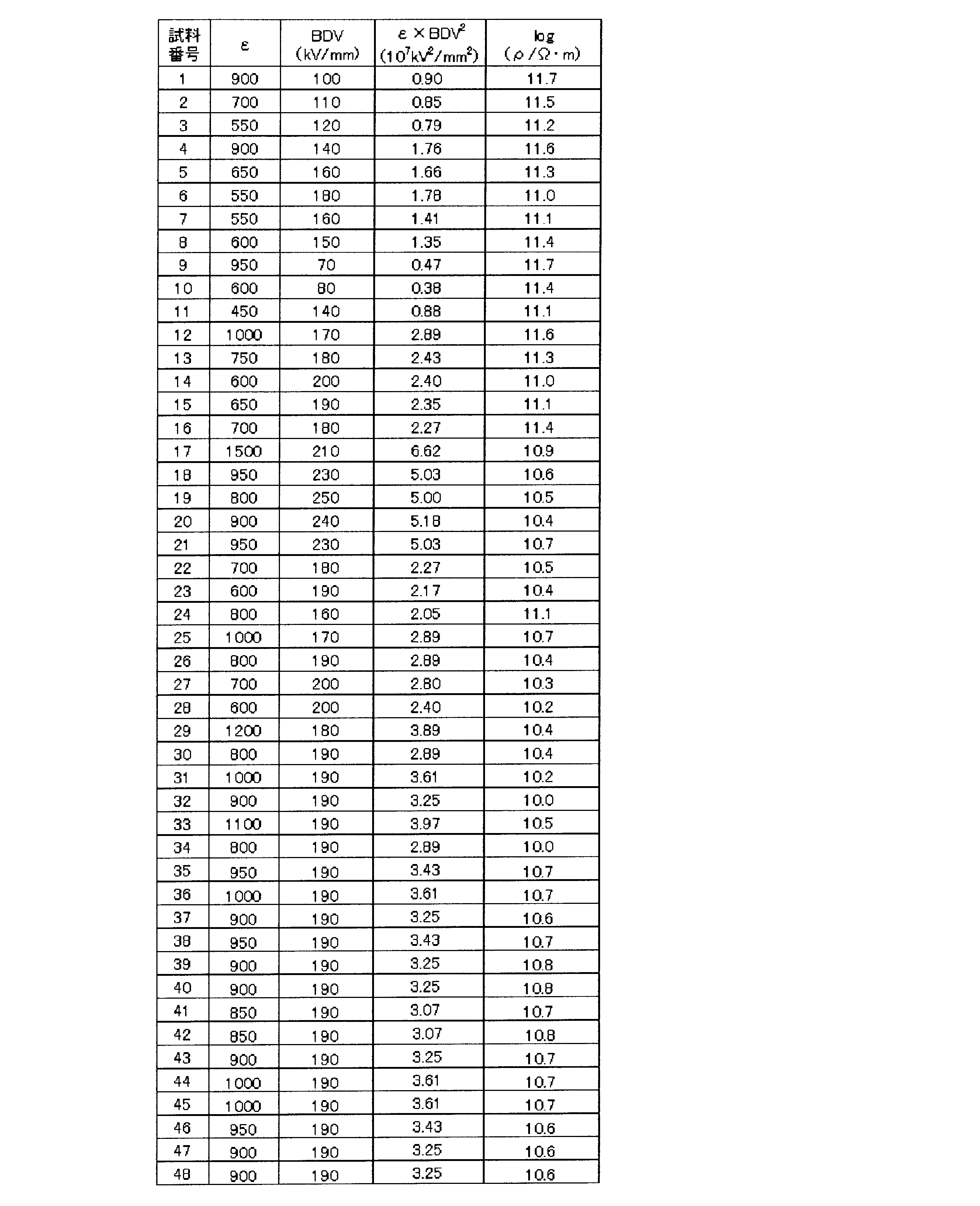
試料番号1~11の試料は、表1に示すように、希土類元素を含まない組成において、(x,y,z)を変化させたものである。これらの試料番号1~11の試料のうち、(x,y,z)が本発明の範囲にある試料番号4~8の試料によれば、500以上のεおよび140kV/mm以上のBDVを得ることができ、中高圧対応の目安である120kV/mmのBDVが保証されることがわかる。ε×(BDV)2としては、1×107kV2/mm2以上の値が得られることがわかる。これに対し、(x,y,z)が本発明の範囲外である試料番号1~3、9~11の試料では、BDVとεがともに高くなく、ε×(BDV)2は、1×107kV2/mm2に満たない値となっていることがわかる。
試料番号12~21の試料は、上述した試料番号4~8の試料と比較しながら、希土類元素としてのDyの添加による効果を評価したものである。試料番号12~21の試料によれば、試料番号4~8の試料と比較して、εおよびBDVがともに向上しており、このことは、ε×(BDV)2において顕著に現れていることがわかる。
試料番号24~28の試料は、希土類元素Dyの添加量を変化させて、添加量による影響を評価するためのものである。希土類元素の添加量が1~14モル部の範囲内において、希土類元素を含まない試料4~8と同等またはそれ以上のεおよびBDVが得られていることがわかる。
試料番号22~23の試料は、mを変化させたものであり、試料番号29~34の試料は、Mg、MnまたはSiの添加量を変化させたものである。mについては0.95~1.025、Mgについて0.5~5.0モル部、Mnについて0.1~3.0モル部、Siについて1.0~5.0モル部の範囲において、還元雰囲気中で焼成された積層セラミックコンデンサにおいても、十分に絶縁性を備え、十分なεとBDVが得られていることがわかる。
試料番号35~48の試料は、希土類元素として、Dy以外のものでも適用可能であることを確認したものである。
今回開示された実施の形態と実施例はすべての点で例示であって制限的なものではないと考慮されるべきである。本発明の範囲は以上の実施の形態と実施例ではなく、請求の範囲によって示され、請求の範囲と均等の意味および範囲内でのすべての修正や変形を含むものであることが意図される。
高い絶縁破壊電圧だけでなく、高い誘電率εを有する誘電体セラミックを得ることができるので、相対的に高い電界下で用いられる中高圧用途に適した積層セラミックコンデンサを提供することができる。
1 積層セラミックコンデンサ
2 積層体
3 誘電体セラミック層
4,5 内部電極層
8,9 外部電極
2 積層体
3 誘電体セラミック層
4,5 内部電極層
8,9 外部電極
Claims (5)
- (BaxSryCaz)TiO3(x、y、zはモル比を表し、x+y+z=1を満たす)を主成分とし、前記(x,y,z)が、三元系組成図において、点A(0.70,0.00,0.30)、点B(0.69,0.02,0.29)、点C(0.55,0.10,0.35)、点D(0.35,0.15,0.50)、および、点E(0.50,0.00,0.50)で構成される五角形ABCDEに囲まれる領域内および線上にある(ただし、点A、点E、および、線分AEを含まない)、誘電体セラミック。
- さらに、Y、La、Ce、Pr、Nd、Sm、Eu、Gd、Tb、Dy、Ho、Er、Tm、YbおよびLuからなる群より選ばれる少なくとも1種の希土類元素を、前記主成分100モル部に対して、1モル部以上14モル部以下含む、請求項1に記載の誘電体セラミック。
- さらに、Mg、MnおよびSiを、それぞれ、前記主成分100モル部に対して、0.1モル部以上3.0モル部以下、0.5モル部以上5.0モル部以下、および、1.0モル部以上5.0モル部以下含む、請求項1または請求項2に記載の誘電体セラミック。
- 積層された複数の誘電体セラミック層と、各々が前記複数の誘電体セラミック層間の特定の界面に沿って形成された複数の内部電極層とを含む積層体と、
前記複数の内部電極層に電気的に接続されるように前記積層体の外表面上に形成された外部電極とを備え、
前記誘電体セラミック層が、請求項1から請求項3までのいずれか1項に記載の誘電体セラミックからなる、積層セラミックコンデンサ。 - 使用電界が25kV/mm以上100kV/mm以下であり、保証絶縁破壊電圧が120kV/mm以上である、請求項4に記載の積層セラミックコンデンサ。
Applications Claiming Priority (2)
| Application Number | Priority Date | Filing Date | Title |
|---|---|---|---|
| JP2008213379A JP2011246284A (ja) | 2008-08-21 | 2008-08-21 | 誘電体セラミックおよび積層セラミックコンデンサ |
| JP2008-213379 | 2008-08-21 |
Publications (1)
| Publication Number | Publication Date |
|---|---|
| WO2010021087A1 true WO2010021087A1 (ja) | 2010-02-25 |
Family
ID=41706980
Family Applications (1)
| Application Number | Title | Priority Date | Filing Date |
|---|---|---|---|
| PCT/JP2009/003458 Ceased WO2010021087A1 (ja) | 2008-08-21 | 2009-07-23 | 誘電体セラミックおよび積層セラミックコンデンサ |
Country Status (2)
| Country | Link |
|---|---|
| JP (1) | JP2011246284A (ja) |
| WO (1) | WO2010021087A1 (ja) |
Cited By (1)
| Publication number | Priority date | Publication date | Assignee | Title |
|---|---|---|---|---|
| CN113410051A (zh) * | 2020-03-16 | 2021-09-17 | 株式会社村田制作所 | 层叠陶瓷电容器 |
Citations (5)
| Publication number | Priority date | Publication date | Assignee | Title |
|---|---|---|---|---|
| JPH06199570A (ja) * | 1992-12-29 | 1994-07-19 | Tdk Corp | 複合ペロブスカイト型セラミック体 |
| JPH06275459A (ja) * | 1993-03-22 | 1994-09-30 | Tdk Corp | 積層型セラミックチップコンデンサ |
| JPH11340075A (ja) * | 1998-05-27 | 1999-12-10 | Philips Japan Ltd | 誘電体磁器組成物 |
| JP3245984B2 (ja) * | 1992-07-24 | 2002-01-15 | 株式会社村田製作所 | 負の抵抗温度特性を有するチタン酸バリウム系半導体磁器及びその製造方法 |
| JP2006237273A (ja) * | 2005-02-24 | 2006-09-07 | Kyocera Corp | 電子部品およびその製造方法並びにこれを用いた携帯電話、デジタルチューナ |
-
2008
- 2008-08-21 JP JP2008213379A patent/JP2011246284A/ja active Pending
-
2009
- 2009-07-23 WO PCT/JP2009/003458 patent/WO2010021087A1/ja not_active Ceased
Patent Citations (5)
| Publication number | Priority date | Publication date | Assignee | Title |
|---|---|---|---|---|
| JP3245984B2 (ja) * | 1992-07-24 | 2002-01-15 | 株式会社村田製作所 | 負の抵抗温度特性を有するチタン酸バリウム系半導体磁器及びその製造方法 |
| JPH06199570A (ja) * | 1992-12-29 | 1994-07-19 | Tdk Corp | 複合ペロブスカイト型セラミック体 |
| JPH06275459A (ja) * | 1993-03-22 | 1994-09-30 | Tdk Corp | 積層型セラミックチップコンデンサ |
| JPH11340075A (ja) * | 1998-05-27 | 1999-12-10 | Philips Japan Ltd | 誘電体磁器組成物 |
| JP2006237273A (ja) * | 2005-02-24 | 2006-09-07 | Kyocera Corp | 電子部品およびその製造方法並びにこれを用いた携帯電話、デジタルチューナ |
Cited By (2)
| Publication number | Priority date | Publication date | Assignee | Title |
|---|---|---|---|---|
| CN113410051A (zh) * | 2020-03-16 | 2021-09-17 | 株式会社村田制作所 | 层叠陶瓷电容器 |
| CN113410051B (zh) * | 2020-03-16 | 2022-07-01 | 株式会社村田制作所 | 层叠陶瓷电容器 |
Also Published As
| Publication number | Publication date |
|---|---|
| JP2011246284A (ja) | 2011-12-08 |
Similar Documents
| Publication | Publication Date | Title |
|---|---|---|
| JP5158071B2 (ja) | 誘電体セラミック組成物及び積層セラミックコンデンサ | |
| JP4805938B2 (ja) | 誘電体磁器およびその製法、並びに積層セラミックコンデンサ | |
| JP5370212B2 (ja) | 誘電体セラミックおよび積層セラミックコンデンサ | |
| JPWO2008155945A1 (ja) | 誘電体セラミック組成物及び積層セラミックコンデンサ | |
| JP2010040798A (ja) | 積層セラミックコンデンサ | |
| WO2011027625A1 (ja) | 誘電体磁器組成物、及び積層セラミックコンデンサ | |
| JP4525680B2 (ja) | 誘電体セラミック組成物および積層セラミックコンデンサ | |
| JP5423682B2 (ja) | 誘電体セラミックおよび積層セラミックコンデンサ | |
| JP2011079717A (ja) | 誘電体セラミックおよび積層セラミックコンデンサ | |
| JP2003277139A (ja) | 誘電体磁器組成物および電子部品 | |
| CN105359236B (zh) | 层叠陶瓷电容器 | |
| JP2010052964A (ja) | 誘電体セラミックおよびその製造方法ならびに積層セラミックコンデンサ | |
| US7239501B2 (en) | Dielectric ceramic composition and laminated ceramic capacitor | |
| WO2012096223A1 (ja) | 積層セラミックコンデンサ及び積層セラミックコンデンサの製造方法 | |
| JP5423785B2 (ja) | 誘電体セラミックおよび積層セラミックコンデンサ | |
| JP2005029423A (ja) | 誘電体磁器組成物および電子部品 | |
| JP4548423B2 (ja) | 誘電体セラミックおよび積層セラミックコンデンサ | |
| JP5307554B2 (ja) | 積層セラミックコンデンサ | |
| JP2008088053A (ja) | 誘電体磁器組成物および電子部品 | |
| CN100390099C (zh) | 介电陶瓷组合物和单片陶瓷电容器 | |
| JP2011184251A (ja) | 誘電体セラミックおよび積層セラミックコンデンサ | |
| WO2010021087A1 (ja) | 誘電体セラミックおよび積層セラミックコンデンサ | |
| JP4752327B2 (ja) | 誘電体セラミック組成物および積層セラミックコンデンサ | |
| JP5729419B2 (ja) | 積層セラミックコンデンサ | |
| JP6372569B2 (ja) | 誘電体セラミックおよび積層セラミックコンデンサ |
Legal Events
| Date | Code | Title | Description |
|---|---|---|---|
| 121 | Ep: the epo has been informed by wipo that ep was designated in this application |
Ref document number: 09808023 Country of ref document: EP Kind code of ref document: A1 |
|
| NENP | Non-entry into the national phase |
Ref country code: DE |
|
| NENP | Non-entry into the national phase |
Ref country code: JP |
|
| 122 | Ep: pct application non-entry in european phase |
Ref document number: 09808023 Country of ref document: EP Kind code of ref document: A1 |