WO2009154015A1 - 半導体装置の検査方法 - Google Patents
半導体装置の検査方法 Download PDFInfo
- Publication number
- WO2009154015A1 WO2009154015A1 PCT/JP2009/052547 JP2009052547W WO2009154015A1 WO 2009154015 A1 WO2009154015 A1 WO 2009154015A1 JP 2009052547 W JP2009052547 W JP 2009052547W WO 2009154015 A1 WO2009154015 A1 WO 2009154015A1
- Authority
- WO
- WIPO (PCT)
- Prior art keywords
- voltage
- upper electrode
- semiconductor device
- lower electrode
- electrode
- Prior art date
- Legal status (The legal status is an assumption and is not a legal conclusion. Google has not performed a legal analysis and makes no representation as to the accuracy of the status listed.)
- Ceased
Links
Images





Classifications
-
- H—ELECTRICITY
- H10—SEMICONDUCTOR DEVICES; ELECTRIC SOLID-STATE DEVICES NOT OTHERWISE PROVIDED FOR
- H10P—GENERIC PROCESSES OR APPARATUS FOR THE MANUFACTURE OR TREATMENT OF DEVICES COVERED BY CLASS H10
- H10P74/00—Testing or measuring during manufacture or treatment of wafers, substrates or devices
- H10P74/20—Testing or measuring during manufacture or treatment of wafers, substrates or devices characterised by the properties tested or measured, e.g. structural or electrical properties
- H10P74/207—Electrical properties, e.g. testing or measuring of resistance, deep levels or capacitance-voltage characteristics
-
- B—PERFORMING OPERATIONS; TRANSPORTING
- B81—MICROSTRUCTURAL TECHNOLOGY
- B81C—PROCESSES OR APPARATUS SPECIALLY ADAPTED FOR THE MANUFACTURE OR TREATMENT OF MICROSTRUCTURAL DEVICES OR SYSTEMS
- B81C99/00—Subject matter not provided for in other groups of this subclass
- B81C99/0035—Testing
- B81C99/0045—End test of the packaged device
-
- H—ELECTRICITY
- H02—GENERATION; CONVERSION OR DISTRIBUTION OF ELECTRIC POWER
- H02N—ELECTRIC MACHINES NOT OTHERWISE PROVIDED FOR
- H02N1/00—Electrostatic generators or motors using a solid moving electrostatic charge carrier
- H02N1/002—Electrostatic motors
- H02N1/006—Electrostatic motors of the gap-closing type
Definitions
- the present invention relates to a method for inspecting a semiconductor device having a micromechanical structure, and more particularly to a technology effective when applied to a method for inspecting a semiconductor device having a device manufactured using MEMS (Micro Electro Mechanical Systems) technology. It is.
- MEMS Micro Electro Mechanical Systems
- MEMS technology using a semiconductor manufacturing process has attracted attention as a basic technology that gives added value to semiconductor products or manufacturing inspection devices.
- Devices already manufactured using MEMS technology (hereinafter simply referred to as MEMS devices) are mounted on various electronic devices, such as various sensors such as pressure sensors, acceleration sensors, and flow sensors, and projectors. It is used for DMD (Digital Micromirror Device), which is a kind of optical element, and minute nozzles in the head of an inkjet printer.
- DMD Digital Micromirror Device
- the MEMS device is composed of an electric control circuit and a mechanical drive unit. Due to this characteristic configuration, the cause of the defect or failure of the MEMS device is due to a mechanism different from that of the conventional semiconductor device. There are many cases. Therefore, establishing a MEMS device inspection method that is different from the semiconductor device inspection method is one of the important issues for improving the reliability of semiconductor products equipped with the MEMS device.
- Patent Document 1 calculates characteristics required for a MEMS device from a usage condition assumed in advance in a microstructure and whether or not the characteristics are satisfied. Based on this, a method for determining a non-defective product / defective product is disclosed. Japanese Patent Laid-Open No. 2007-40896
- a non-defective / defective product determination method for an initial failure described in Patent Document 1 As a method for inspecting a semiconductor device on which a MEMS device is mounted, a non-defective / defective product determination method for an initial failure described in Patent Document 1 is performed.
- an effective non-defective / defective product determination method for accidental failures and wear failures due to aging has not been established yet, including elucidation of technical mechanisms. For example, it is possible to determine whether a non-defective product or a defective product by actually mechanically driving the MEMS device until a time to be guaranteed against a wear failure due to accidental failure or aging deterioration.
- this determination method requires an enormous amount of inspection time, the manufacturing cost increases with the increase in inspection time. Further, if the number of inspections is reduced in order to reduce the manufacturing cost, the reliability of the semiconductor device on which the MEMS device is mounted cannot be guaranteed.
- An object of the present invention is to provide a technique capable of improving the reliability of a semiconductor device on which a MEMS device is mounted.
- This embodiment is an inspection method of an ultrasonic transducer on which a MEMS device is mounted.
- the lower limit operation number of the upper electrode at which the lowering of the withstand voltage does not occur between the lower electrode and the upper electrode constituting the MEMS device is determined, the inspection voltage is determined, and the reference between the lower electrode and the upper electrode is determined. Determine the dielectric strength.
- an inspection voltage is applied, and the upper electrode is operated more than the lower limit number of operations of the upper electrode.
- the withstand voltage between the lower electrode and the upper electrode is measured below the reference withstand voltage, and the non-defective / defective product of the semiconductor device is determined using the obtained withstand voltage.
- the reliability of a semiconductor device equipped with a MEMS device can be improved.
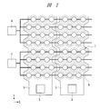
- FIG. 1 is an overall plan view of a semiconductor chip constituting an ultrasonic transducer according to an embodiment of the present invention. It is a principal part top view which expands and shows a part of FIG. It is principal part sectional drawing of the MEMS device mounted in the ultrasonic transducer by one embodiment of this invention. It is a graph which shows the capacity-voltage characteristic of the ultrasonic transducer by one embodiment of the present invention. It is a graph explaining the withstand voltage of the insulating film between the lower electrode and upper electrode which comprise the MEMS device mounted in the ultrasonic transducer by one embodiment of this invention.
- (A) is a graph showing the measurement result of current-voltage between the lower electrode and the upper electrode before voltage is applied, and (b) is between the lower electrode and the upper electrode after voltage is applied. It is a graph which shows the measurement result of current-voltage. It is a flowchart figure of the inspection method of the ultrasonic transducer by one embodiment of the present invention. It is a graph which shows the relationship between the shift amount of the capacity-voltage curve and AC voltage (Vp-p) by one embodiment of this invention. It is a graph which shows the relationship between the defect rate by one embodiment of this invention, and a withstand voltage. It is a graph which shows the relationship between the reference dielectric strength voltage and the frequency
- a method for inspecting a semiconductor device equipped with a MEMS device according to an embodiment of the present invention will be described below.
- the invention made by the present inventors is applied to an inspection method for an ultrasonic transducer mounted with a MEMS device, which is a field of use as a background.
- FIGS. 1 is an overall plan view of a semiconductor chip constituting an ultrasonic transducer according to an embodiment of the present invention
- FIG. 2 is an enlarged plan view of a main part showing a part of FIG. 1
- FIG. 3 is an embodiment of the present invention. It is principal part sectional drawing of the sensor element (MEMS device) mounted in the ultrasonic transducer by a form.
- MEMS device sensor element
- a sensor element array region 2 and a plurality of bonding pads 3 and 4 are arranged on a semiconductor chip 1.
- a plurality of lower electrode wirings and a plurality of upper electrode wirings orthogonal thereto are arranged.
- each of the plurality of lower electrode wirings 5 is formed along a first direction (long side direction, Y direction in FIGS. 1 and 2) of the semiconductor chip 1.
- 16 channels are arranged side by side in a second direction (short side direction, X direction in FIGS. 1 and 2) orthogonal to one direction.
- Each of the plurality of lower electrode wirings 5 is electrically connected to the bonding pad 3.
- a plurality of bonding pads 3 are arranged side by side along the second direction of the semiconductor chip 1 on the outer periphery of the sensor element array region 2.
- the plurality of upper electrode wirings 6 are respectively formed along the second direction of the semiconductor chip 1, and are arranged side by side, for example, 192 channels in the first direction of the semiconductor chip 1. Each of the plurality of upper electrode wirings 6 is electrically connected to the bonding pad 4. A plurality of bonding pads 4 are arranged side by side along the first direction of the semiconductor chip 1 on the outer periphery of the sensor element array region 2.
- the MEMS device 7 is, for example, an electrostatic variable capacitance element, and is disposed at the intersection of the lower electrode wiring 5 and the upper electrode wiring 6. That is, the plurality of MEMS devices 7 are regularly arranged in an array in the sensor element array region 2.
- the shape of the MEMS device 7 is hexagonal, and, for example, twelve MEMS devices 7 are arranged in a honeycomb shape at the intersection of the lower electrode wiring 5 and the upper electrode wiring 6 in the sensor element array region 2.
- the MEMS device 7 includes a lower electrode 5a, a cavity 11 formed on the lower electrode 5a so as to overlap the lower electrode 5a when viewed from the upper surface, and a cavity 11 formed on the cavity 11 and viewed from the upper surface. And an insulating film (second insulating film 10 and third insulating film formed between the lower electrode 5a and the cavity 11 and between the cavity 11 and the upper electrode 6a, respectively.
- Membrane 12 the MEMS device 7 includes a lower electrode 5a, a cavity 11 formed on the lower electrode 5a so as to overlap the lower electrode 5a when viewed from the upper surface, and a cavity 11 formed on the cavity 11 and viewed from the upper surface.
- an insulating film (second insulating film 10 and third insulating film formed between the lower electrode 5a and the cavity 11 and between the cavity 11 and the upper electrode 6a, respectively.
- Membrane 12 membrane 12
- the lower electrode 5 a is formed by a part of the lower electrode wiring 5 described above, and is a portion of the lower electrode wiring 5 that overlaps the upper electrode wiring 6 in a plane, that is, a portion that is located below the upper electrode wiring 6. .
- a second insulating film 10 is formed so as to cover the lower electrode 5a. Furthermore, a third insulating film 12 is formed on the second insulating film 10 via the cavity 11.
- the upper electrode 6 a is formed by a part of the upper electrode wiring 6 described above, and is a portion of the upper electrode wiring 6 that overlaps the lower electrode wiring 5 in a plane, that is, a portion positioned above the lower electrode wiring 5. .
- the planar shape of the upper electrode 6a is a hexagon.
- the second insulating film 10 is disposed between the lower electrode 5a and the cavity 11, and has a role of ensuring insulation resistance between the lower electrode 5a and the upper electrode 6a.
- the third insulating film 12 is disposed between the cavity portion 11 and the upper electrode 6a, and has a role of ensuring insulation resistance between the lower electrode 5a and the upper electrode 6a together with the second insulating film 10. Yes.
- a fourth insulating film 13 and a fifth insulating film 14 are sequentially formed so as to cover the upper electrode 6a.
- the second insulating film 10 is provided between the lower electrode 5a and the cavity 11, and the third insulating film 12 is further provided between the cavity 11 and the upper electrode 6a. Only one of them may be provided.
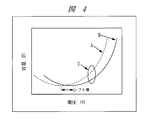
- FIG. 4 is a graph showing the capacitance-voltage characteristics of the ultrasonic transducer according to the embodiment of the present invention
- FIG. 5 is a lower electrode and an upper electrode constituting the MEMS device mounted on the ultrasonic transducer according to the embodiment of the present invention. It is a graph explaining the withstand voltage of the insulating film between.
- the third insulating film 12 and the upper electrode 6a constitute a membrane, and this membrane vibrates.
- a DC voltage and an AC voltage are applied in a superimposed manner between the lower electrode 5a and the upper electrode 6a, an electrostatic force acts between the lower electrode 5a and the upper electrode 6a, and the membrane on the cavity 11 has an applied AC voltage. It can vibrate in a direction intersecting the semiconductor substrate 8 at a frequency and can transmit (transmit) an ultrasonic wave.
- the membrane on the cavity 11 of each MEMS device 7 vibrates due to the pressure of the ultrasonic wave reaching the surface of the sensor element array region 2. Due to this vibration, the distance (interval) between the lower electrode 5a and the upper electrode 6a changes, so that an ultrasonic wave can be detected as a change in electric capacity between the lower electrode 5a and the upper electrode 6a. That is, when the distance (interval) between the lower electrode 5a and the upper electrode 6a changes, the electric capacity between the lower electrode 5a and the upper electrode 6a changes, and an alternating current flows. By detecting this current, ultrasonic waves can be detected.
- ultrasonic transducers it is desirable for ultrasonic transducers to have high ultrasonic transmission / reception sensitivity.
- the shape of the membrane is a hexagon inscribed in a circle having a diameter of 60 ⁇ m
- the thickness of each of the second insulating film 10 and the third insulating film 12 is 200 nm
- the thickness is 100 nm
- the distance (interval) between the second insulating film 10 and the third insulating film 12 sandwiching the cavity 11 when a voltage is applied between the lower electrode 5a and the upper electrode 6a is the lower electrode 5a and the upper electrode 6a.
- the distance between the second insulating film 10 and the third insulating film 12 is about 2/3.
- the membrane is operated by contact with the insulating film 12. Such contact between the second insulating film 10 and the third insulating film 12 causes the following two problems.
- the first problem is that the transmission / reception sensitivity decreases when the membrane contacts the second insulating film 10.
- a high electric field is applied between the lower electrode 5a and the upper electrode 6a, and a current flows through the second insulating film 10 or the third insulating film 12.
- charges are trapped in the trap of the second insulating film 10 or the third insulating film 12.
- the lines of electric force between the lower electrode 5a and the upper electrode 6a are terminated by the charges trapped in the traps of the second insulating film 10 or the third insulating film 12, and the lower electrode 5a and the upper electrode 6a The effective electric field between them becomes small.
- FIG. 4 is a graph showing the measurement result of the capacity-voltage curve (A) when no charge accumulation occurs and the measurement result of the capacity-voltage curve (B) when charge accumulation occurs.
- the capacitance-voltage curve (B) in the case where charges are accumulated in the second insulating film 10 or the third insulating film 12 is the case where charges are not accumulated in the second insulating film 10 or the third insulating film 12 (voltage Compared with the capacitance-voltage curve (A) before (a) is applied, the whole is shifted to the high voltage side (right side of the graph shown in FIG. 4). This means that the voltage applied between the lower electrode 5a and the upper electrode 6a is effectively reduced as described above.
- the shift of the capacitance-voltage curve corresponds to, for example, a decrease in transmission / reception sensitivity (corresponding to the slope of the capacitance-voltage curve) at the operating point C in the figure, and the membrane contacts the second insulating film 10. This means that when the MEMS device 7 is repeatedly operated, the transmission / reception sensitivity decreases with time.
- the second problem is that when the second insulating film 10 and the third insulating film 12 come into contact with each other with a voltage applied, the dielectric strength voltage of the second insulating film 10 or the third insulating film 12 is lowered, resulting in dielectric breakdown. It is to reach.
- FIG. 5A is a graph showing a measurement result of current-voltage between the lower electrode 5a and the upper electrode 6a before voltage is applied
- FIG. 5B is a diagram showing the membrane in contact with the second insulating film 10. It is a graph which shows the measurement result of the electric current-voltage between the lower electrode 5a and the upper electrode 6a after making it operate
- the inspection voltage in consideration of the contact between the membrane and the second insulating film 10 and the breakdown voltage deterioration of the second insulating film 10 or the third insulating film 12.
- the height of the cavity 11 of the MEMS device 7 includes variations. Therefore, for the inspection of the ultrasonic transducer, it is necessary to inspect whether or not the membrane is in contact with the second insulating film 10 by using the actual operating voltage as the inspection voltage. As described above, when the membrane comes into contact with the second insulating film 10, charges are accumulated in the second insulating film 10 or the third insulating film 12.
- the capacitance-voltage curve is measured and the capacitance-voltage curve shifts.
- the presence or absence of the contact can be confirmed by the presence or absence of.
- the ultrasonic transducer it is difficult to measure a minute capacitance change with each MEMS device 7. Therefore, in the ultrasonic transducer inspection method as the background of the present invention, the dielectric strength of the second insulating film 10 or the third insulating film 12 varies greatly depending on whether or not the membrane and the second insulating film 10 are in contact with each other. By using this, it is determined whether the ultrasonic transducer is good or defective.
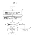
- FIG. 6 is a flowchart of the ultrasonic transducer inspection method according to the embodiment of the present invention
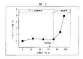
- FIG. 7 shows the relationship between the shift amount of the capacitance-voltage curve and the AC voltage (Vp-p) according to the embodiment of the present invention
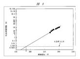
- FIG. 8 is a graph showing the relationship between the defect rate and the withstand voltage according to the embodiment of the present invention
- FIG. 9 is a graph showing the relationship between the reference withstand voltage and the number of vibrations of the membrane according to the embodiment of the present invention.
- FIG. 10 and FIG. 10 are graphs showing the relationship between the withstand voltage and the membrane vibration frequency according to the embodiment of the present invention.
- an inspection voltage (an AC voltage and a DC voltage) at which the membrane and the second insulating film 10 do not contact is determined.
- the capacitance-voltage curve shown in FIG. 4 is measured, and the inspection voltage is determined from the shift amount.
- FIG. 7 is a graph showing an example of the relationship between the shift amount of the capacity-voltage curve and the AC voltage (Vp-p).
- the AC voltage is 0 to 96 V (Vp-p) and the membrane is vibrated 10 10 times. It is a measurement result at the time.
- the DC voltage is considered to be in the appropriate range of 70% to 90% centered on 80% of the voltage at which the membrane contacts the second insulating film 10 (collapse voltage). Of course, the voltage is set to 90V. From FIG.
- a capacitance-voltage curve shift occurs at an AC voltage of about 70 V (Vp-p) or more, and this voltage is a voltage at which the membrane and the second insulating film 10 are in contact with each other. From this result, the inspection voltage is lower than about 70 (Vp-p), which is a voltage at which the membrane and the second insulating film 10 are in contact with each other in consideration of a variation in the collapse voltage between adjacent MEMS devices 7.
- the voltage can be determined, for example 60V.
- the reference dielectric strength that will be the criterion.
- an insulating film for example, the second insulating film 10 and the third insulating film 12
- the reference dielectric strength is obtained by statistically processing the obtained plurality of measurement results. For example, as shown in FIG.
- the relationship between the defect rate and the withstand voltage is graphed by a wipe plot, and the defect rate defined as a non-defective product in the inspection by extrapolating the wipe plot is, for example, a defect rate of 0.1%
- An insulation withstand voltage A is obtained and used as a reference withstand voltage.
- FIG. 9 is a graph showing an example of the relationship between the reference withstand voltage and the number of membrane vibrations. It can be seen that when the number of vibrations of the membrane is up to 10 10 times, the withstand voltage deteriorates as the number of vibrations increases. However, when the number of vibrations of the membrane is 10 10 times or more, almost no deterioration of the withstand voltage is observed. The reason why the withstand voltage does not deteriorate when the number of vibrations of the membrane is 10 10 times or more can be estimated as follows. That is, when the membrane vibrates under the condition of contact with the membrane, the electric charge is captured by the trap of the second insulating film 10 or the third insulating film 12.
- the electric lines of force between the lower electrode 5a and the upper electrode 6a are terminated by the electric charge of the second insulating film 10 or the third insulating film 12, and the effective electric field between the lower electrode 5a and the upper electrode 6a.
- the electric field is reduced. Therefore, the membrane does not come into contact with the second insulating film 10 while repeatedly vibrating.
- the capacitance-voltage curve shifts to the high voltage side, the capacitance at the operating point C decreases, and the distance (interval) between the lower electrode 5a and the upper electrode 6a increases. The membrane does not come into contact with the second insulating film 10.
- the inspection voltage AC voltage and DC voltage
- the reference dielectric strength and the membrane vibration frequency obtained in this way, the AC voltage and DC voltage were superimposed on the ultrasonic transducer and applied to the membrane.
- the lower limit membrane vibration frequency at which the withstand voltage does not decrease is obtained, and the inspection voltage (AC voltage and DC voltage) and the reference withstand voltage are determined.
- FIG. 10 shows an example of the result of summarizing the inspection voltage (AC voltage and DC voltage), the reference withstand voltage, and the membrane vibration frequency. From the results shown in FIG. 10, for example, the lower limit number of times that the dielectric breakdown voltage does not decrease in the membrane can be determined as 10 10 times. Further, for example, the inspection voltage (actual operating voltage) is 120V (DC voltage 90V + AC voltage) 60 ⁇ 1 / 2V) and the reference dielectric strength can be determined to be 180V.
- a semiconductor wafer having a plurality of ultrasonic transducers formed on the main surface is prepared.
- the MEMS device 7 is driven a predetermined number of times (for example, 10 10 times) by superimposing and applying the inspection voltage determined by the above-described method to all or some of the ultrasonic transducers formed on the main surface of the semiconductor wafer. (Step P1 in FIG. 6).
- a DC voltage is swept to a predetermined voltage that is equal to or higher than the inspection voltage (actual operating voltage) (for example, 120 V or higher) and equal to or lower than the reference dielectric strength voltage (for example, 180 V or lower).
- the current value at that time is monitored.
- a DC voltage is applied to all or a part of the ultrasonic transducers for a predetermined time in a voltage range of an inspection voltage (actual operating voltage) or more (for example, 120 V or more) and a reference dielectric strength voltage (for example, 180 V or less), The presence or absence of dielectric breakdown is checked (step P2 in FIG. 6).
- step P3 the ultrasonic transducer in which dielectric breakdown did not occur is determined as a non-defective product (step P4 in FIG. 6), and the ultrasonic transducer in which dielectric breakdown has occurred is determined as defective (step P5 in FIG. 6). For example, a defective marking is applied to a semiconductor chip on which an ultrasonic transducer determined to be defective is formed.
- the semiconductor wafer is diced to separate the semiconductor wafer into semiconductor chips.
- a semiconductor wafer is cut vertically and horizontally along a scribe line by using an extremely thin circular blade with diamond fine particles called diamond saw attached thereto.
- the semiconductor chip determined to be a non-defective product in the above-described inspection process is protected by, for example, a mold resin, and a product is completed through a plurality of processes such as an inspection process for selecting the semiconductor chip in accordance with product standards.
- non-defective / defective products caused by accidental failures or wear failures due to aging degradation of all or some of the ultrasonic transducers are formed on the main surface of the semiconductor wafer. It can be determined in a short time. Thereby, since the defective product can be selected and removed at an early stage before the ultrasonic transducer is mounted on the product, the reliability of the ultrasonic transducer can be improved. Furthermore, the product cost of the ultrasonic transducer can be reduced.
- all or a part of the ultrasonic transducers are judged as non-defective / defective in a state where they are formed on the main surface of the semiconductor wafer.
- the inspection method according to the present invention can also be applied to the determination of non-defective / defective products. As a result, 100% inspection of the products can be performed in a short time, and therefore a product that is inexpensive and highly reliable can be provided.
- the present invention is applied to an inspection method of an ultrasonic transducer in which a capacitive MEMS device having a membrane structure is mounted.
- the present invention is not limited to this.
- the present invention can also be applied to an inspection method for an ultrasonic transducer on which a capacitive MEMS device is mounted.
- the object is not limited to the ultrasonic transducer, and can be applied to an inspection method of a semiconductor device on which a MEMS device for other uses is mounted.
- the present invention can be applied to a method for inspecting a semiconductor device on which a MEMS device is mounted. It can also be used as an inspection sequence of an inspection apparatus for inspecting a semiconductor device on which a MEMS device is mounted.
Landscapes
- Engineering & Computer Science (AREA)
- Microelectronics & Electronic Packaging (AREA)
- Micromachines (AREA)
- Pressure Sensors (AREA)
- Transducers For Ultrasonic Waves (AREA)
Abstract
MEMSデバイスを構成する下部電極と上部電極との間で絶縁耐圧の低下が生じなくなる上部電極の下限の動作回数を求め、検査電圧を決定し、そして下部電極と上部電極との間の基準絶縁耐圧を決定した後、検査電圧を印加して上部電極の下限の動作回数以上、上部電極を動作させる。その後、基準絶縁耐圧以下で、下部電極と上部電極との間の絶縁耐圧を測定し、得られた絶縁耐圧を用いて半導体装置の良品/不良品の判定を行う。
Description
本発明は、微小機械構造体を有する半導体装置の検査方法に関し、特に、MEMS(Micro Electro Mechanical Systems)技術を用いて製造されたデバイスを有する半導体装置の検査方法に適用して有効な技術に関するものである。
近年、半導体製造プロセスを利用したMEMS技術が、半導体製品または製造検査装置などに付加価値を与える基盤技術として注目されている。すでにMEMS技術を用いて製造されたデバイス(以下、単にMEMSデバイスと記す)は、様々な電子機器に搭載されており、例えば圧力センサ、加速度センサ、流量センサなどの各種センサや、プロジェクタに搭載されている光学素子の一種であるDMD(Digital Micromirror Device)や、インクジェットプリンタのヘッド部にある微小ノズルなどに利用されている。
ところで、MEMSデバイスは電気的な制御回路と機械的な駆動部とから構成されており、この特徴的な構成のため、MEMSデバイスの不良や故障の原因が、従来の半導体デバイスとは異なるメカニズムによる場合が多い。そのため、半導体デバイスの検査方法とは異なるMEMSデバイスの検査方法を確立することが、MEMSデバイスを搭載した半導体製品の信頼性を向上させる重要な課題の1つとなっている。
特に、機械的な駆動特性を担う可動部や空洞部の製造工程における加工ばらつきは、MEMSデバイスの特性に大きく影響を与えるばかりでなく、MEMSデバイスの初期不良や摩耗故障の原因となっている。従って、製造工程の早い段階で、MEMSデバイスの不良品を選別して除去することが、MEMSデバイスを搭載した半導体製品の製品コストを低減し、信頼性を向上させる効果的な対策となると考えられる。また、出荷する際の良品/不良品の判定方法を確立することも、安価で信頼度の高いMEMSデバイスを搭載した半導体製品を得ることのできる有効な対策となる。
例えば、特開2007-40896号公報(特許文献1)には、微小構造体において、予め想定される使用条件などからMEMSデバイスに要求される特性を算出し、その特性を満たしているか否かに基づいて、良品/不良品を判定する方法が開示されている。
特開2007-40896号公報
一般に、半導体製品を出荷する際には良品/不良品の判定が必要となる。半導体製品において選別すべき不良や故障には、主として以下の3つがある。(1)デバイスを製造した直後の初期不良、(2)デバイス寿命までの間に一定の確率で生じる偶発故障、(3)デバイス寿命の時期に頻繁にみられる経年劣化による摩耗故障である。半導体製品を出荷する前にその全数を検査することが理想的ではあるが、検査数が増加すると製品コストも増加するため、半導体製品の全数を検査することは難しい。そこで、現在は拭き取り検査を実施し、得られた結果を基に半導体製品の信頼度を保証している。
MEMSデバイスを搭載した半導体装置の検査方法としては、前述の特許文献1に記載された初期故障に対する良品/不良品の判定方法が実施されている。しかしながら、偶発故障や経年劣化による摩耗故障に対する有効な良品/不良品の判定方法は、未だ技術的なメカニズムの解明を含めて確立されていない。例えば偶発故障や経年劣化による摩耗故障に対して、保証されるべき時間までMEMSデバイスを実際に機械的に駆動させて、良品/不良品の判定を行うことは可能ではある。しかし、この判定方法は膨大な検査時間を要するため、検査時間の増加に伴う製造コストの増加を招いてしまう。また、製造コストを下げるために検査数を少なくすると、MEMSデバイスを搭載する半導体装置の信頼度を保証することができなくなってしまう。
本発明の目的は、MEMSデバイスを搭載する半導体装置の信頼度を向上させることのできる技術を提供することにある。
本発明の前記ならびにその他の目的と新規な特徴は、本明細書の記述および添付図面から明らかになるであろう。
本願において開示される発明のうち、代表的なものの一実施の形態を簡単に説明すれば、次のとおりである。
この実施の形態は、MEMSデバイスを搭載する超音波トランスデューサの検査方法である。まず、MEMSデバイスを構成する下部電極と上部電極との間で絶縁耐圧の低下が生じなくなる上部電極の下限の動作回数を求め、検査電圧を決定し、そして下部電極と上部電極との間の基準絶縁耐圧を決定する。次に、検査電圧を印加して上部電極の下限の動作回数以上、上部電極を動作させる。次に、基準絶縁耐圧以下で、下部電極と上部電極との間の絶縁耐圧を測定し、得られた絶縁耐圧を用いて半導体装置の良品/不良品の判定を行う。
本願において開示される発明のうち、代表的なものの一実施の形態によって得られる効果を簡単に説明すれば以下のとおりである。
MEMSデバイスを搭載する半導体装置の信頼度を向上させることができる。
1 半導体チップ
2 センサ素子アレイ領域
3,4 ボンディングパッド
5 下部電極配線
5a 下部電極
6 上部電極配線
6a 上部電極
7 MEMSデバイス
8 半導体基板
9 第1絶縁膜
10 第2絶縁膜
11 空洞部
12 第3絶縁膜
13 第4絶縁膜
14 第5絶縁膜
2 センサ素子アレイ領域
3,4 ボンディングパッド
5 下部電極配線
5a 下部電極
6 上部電極配線
6a 上部電極
7 MEMSデバイス
8 半導体基板
9 第1絶縁膜
10 第2絶縁膜
11 空洞部
12 第3絶縁膜
13 第4絶縁膜
14 第5絶縁膜
以下の実施の形態において、便宜上その必要があるときは、複数のセクションまたは実施の形態に分割して説明するが、特に明示した場合を除き、それらはお互いに無関係なものではなく、一方は他方の一部または全部の変形例、詳細、補足説明等の関係にある。
また、以下の実施の形態において、要素の数等(個数、数値、量、範囲等を含む)に言及する場合、特に明示した場合および原理的に明らかに特定の数に限定される場合等を除き、その特定の数に限定されるものではなく、特定の数以上でも以下でも良い。さらに、本実施の形態において、その構成要素(要素ステップ等も含む)は、特に明示した場合および原理的に明らかに必須であると考えられる場合等を除き、必ずしも必須のものではないことは言うまでもない。同様に、以下の実施の形態において、構成要素等の形状、位置関係等に言及するときは、特に明示した場合および原理的に明らかにそうでないと考えられる場合等を除き、実質的にその形状等に近似または類似するもの等を含むものとする。このことは、上記数値および範囲についても同様である。
また、以下の実施の形態を説明するための全図において、同一機能を有するものは原則として同一の符号を付し、その繰り返しの説明は省略する。以下、本発明の実施の形態を図面に基づいて詳細に説明する。
本発明の実施の形態によるMEMSデバイスを搭載する半導体装置の検査方法について以下に説明する。本発明の実施の形態では、本発明者らによってなされた発明を、その背景となった利用分野であるMEMSデバイスを搭載する超音波トランスデューサの検査方法に適用した場合について説明する。
まず、本発明の実施の形態によるMEMSデバイスを搭載する超音波トランスデューサの構造について図1~図3を用いて説明する。図1は本発明の実施の形態による超音波トランスデューサを構成する半導体チップの全体平面図、図2は前記図1の一部を拡大して示す要部平面図、図3は本発明の実施の形態による超音波トランスデューサに搭載されたセンサ素子(MEMSデバイス)の要部断面図である。
図1に示すように、半導体チップ1には、センサ素子アレイ領域2と、複数のボンディングパッド3,4とが配置されている。また、センサ素子アレイ領域2には、複数の下部電極配線と、これに直交する複数の上部電極配線とが配置されている。
図2に示すように、複数の下部電極配線5はそれぞれ半導体チップ1の第1方向(長辺方向、図1および図2中のY方向)に沿って形成されており、半導体チップ1の第1方向と直交する第2方向(短辺方向、図1および図2中のX方向)に、例えば16チャネル(channel)並んで配置されている。複数の下部電極配線5はそれぞれボンディングパッド3と電気的に接続されている。ボンディングパッド3は、センサ素子アレイ領域2の外周部の半導体チップ1の第2方向に沿って複数並んで配置されている。
複数の上部電極配線6はそれぞれ半導体チップ1の第2方向に沿って形成されており、半導体チップ1の第1方向に、例えば192チャネル並んで配置されている。複数の上部電極配線6はそれぞれボンディングパッド4と電気的に接続されている。ボンディングパッド4は、センサ素子アレイ領域2の外周部の半導体チップ1の第1方向に沿って複数並んで配置されている。
MEMSデバイス7は、例えば静電型可変容量素子であり、下部電極配線5と上部電極配線6との交点に配置されている。すなわち、複数のMEMSデバイス7がセンサ素子アレイ領域2内にアレイ状に規則的に並んで配置されている。MEMSデバイス7の形状は六角形であり、センサ素子アレイ領域2内の下部電極配線5と上部電極配線6との交点には、例えば12個のMEMSデバイス7がハニカム状に配置されている。
図3に示すように、MEMSデバイス7は、半導体基板8の主面上に第1絶縁膜9を介して下部電極5aと上部電極6aとが対向し、下部電極5aと上部電極6aとの間に第2絶縁膜10、空洞部11および第3絶縁膜12が介在した構造となる。すなわち、MEMSデバイス7は、下部電極5aと、下部電極5a上に、上面から見て下部電極5aと重なるように形成された空洞部11と、空洞部11上に、上面から見て空洞部11と重なるように形成された上部電極6aと、下部電極5aと空洞部11との間および空洞部11と上部電極6aとの間にそれぞれ形成された絶縁膜(第2絶縁膜10および第3絶縁膜12)とから構成される。
下部電極5aは前述の下部電極配線5の一部により形成されており、下部電極配線5のうち、上部電極配線6と平面的に重なる部分、すなわち上部電極配線6の下方に位置する部分となる。下部電極5aを覆うように第2絶縁膜10が形成されている。さらに、第2絶縁膜10上には、空洞部11を介して第3絶縁膜12が形成されている。
上部電極6aは前述の上部電極配線6の一部により形成されており、上部電極配線6のうち、下部電極配線5と平面的に重なる部分、すなわち下部電極配線5の上方に位置する部分となる。上部電極6aの平面形状は六角形である。
第2絶縁膜10は下部電極5aと空洞部11との間に配置され、下部電極5aと上部電極6aとの間の絶縁耐性を確保する役目を有している。また、第3絶縁膜12は空洞部11と上部電極6aとの間に配置され、第2絶縁膜10とともに、下部電極5aと上部電極6aとの間の絶縁耐性を確保する役目を有している。上部電極6aを覆うように第4絶縁膜13および第5絶縁膜14が順次形成されている。なお、本実施の形態では、下部電極5aと空洞部11との間に第2絶縁膜10を設け、さらに空洞部11と上部電極6aとの間に第3絶縁膜12を設けたが、どちらか一方のみを設けてもよい。
次に、本発明の実施の形態によるMEMSデバイスを搭載する超音波トランスデューサの動作について図4および図5を用いて説明する。図4は本発明の実施の形態による超音波トランスデューサの容量-電圧特性を示すグラフ図、図5は本発明の実施の形態による超音波トランスデューサに搭載されたMEMSデバイスを構成する下部電極と上部電極との間の絶縁膜の絶縁耐圧を説明するグラフ図である。
超音波トランスデューサに搭載されたMEMSデバイス7においては、第3絶縁膜12と上部電極6aとがメンブレンを構成し、このメンブレンが振動する。下部電極5aと上部電極6aとの間に直流電圧および交流電圧を重畳印加すると、下部電極5aと上部電極6aとの間に静電気力が働き、空洞部11上のメンブレンが、印加した交流電圧の周波数で半導体基板8と交差する方向に振動し、超音波を発信(送信)することができる。
逆に、超音波を受信する場合は、センサ素子アレイ領域2の表面に到達した超音波の圧力により、各MEMSデバイス7の空洞部11上のメンブレンが振動する。この振動により、下部電極5aと上部電極6aとの間の距離(間隔)が変化するので、下部電極5aと上部電極6aとの間の電気容量の変化として超音波を検出することができる。すなわち、下部電極5aと上部電極6aとの間の距離(間隔)が変化することにより、下部電極5aと上部電極6aとの間の電気容量が変わり、交流電流が流れる。この電流を検知することにより超音波を検出することができる。
超音波トランスデューサにおいては、超音波の送受信感度が大きいことが望ましい。超音波の送受信感度を大きくするには、送信の面から見ると、メンブレンの振動を大きくして高い送信音圧を得ることが必要となる。メンブレンは下部電極5aと上部電極6aとの間に印加した電圧により振動するので、印加電圧を大きくすると送信音圧が高くなる。つまり、送信音圧を高くするためには、例えばメンブレンの形状が直径60μmの円に内接する六角形で、第2絶縁膜10および第3絶縁膜12の厚さがそれぞれ200nm、空洞部11の厚さが100nmの場合、下部電極5aと上部電極6aとの間に100V以上の高い電圧を印加することが必要となる。
しかし、下部電極5aと上部電極6aとの間に電圧を印加した場合の空洞部11を挟む第2絶縁膜10と第3絶縁膜12との距離(間隔)が、下部電極5aと上部電極6aとの間に電圧を印加していない場合の空洞部11を挟む第2絶縁膜10と第3絶縁膜12との距離(間隔)の2/3程度になると、第2絶縁膜10と第3絶縁膜12とが接触して、メンブレンが動作することになる。このような第2絶縁膜10と第3絶縁膜12との接触は、以下に述べる2つの問題を引き起こす。
一つ目の問題は、メンブレンが第2絶縁膜10に接触すると送受信感度が低下することである。電圧が印加された状態でメンブレンが第2絶縁膜10に接触すると、下部電極5aと上部電極6aとの間に高電界が印加され、第2絶縁膜10または第3絶縁膜12に電流が流れて、電荷が第2絶縁膜10または第3絶縁膜12のトラップに捕獲される。その結果、下部電極5aと上部電極6aとの間の電気力線が第2絶縁膜10または第3絶縁膜12のトラップに捕獲された電荷に終端されて、下部電極5aと上部電極6aとの間の実効的な電界が小さくなる。
図4は、電荷蓄積が生じていない場合の容量-電圧カーブ(A)の測定結果および電荷蓄積が生じている場合の容量-電圧カーブ(B)の測定結果を示すグラフ図である。第2絶縁膜10または第3絶縁膜12に電荷が蓄積されている場合の容量-電圧カーブ(B)は、第2絶縁膜10または第3絶縁膜12に電荷が蓄積されていない場合(電圧が印加される前)の容量-電圧カーブ(A)と比べて全体的に高電圧側(図4に示すグラフ図の右側)にシフトしている。このことは、前述したように、下部電極5aと上部電極6aとの間に印加される電圧が実効的に小さくなっていることを意味している。また、容量-電圧カーブがシフトすることは、例えば図中の動作点Cでの送受信感度(容量-電圧カーブの傾きに相当)が低下することに相当し、メンブレンを第2絶縁膜10に接触させて、MEMSデバイス7を繰り返し動作させると、時間が経つにつれて送受信感度が低下することを意味している。
二つ目の問題は、電圧が印加された状態で第2絶縁膜10と第3絶縁膜12とが接触すると第2絶縁膜10または第3絶縁膜12の絶縁耐圧が低下して、絶縁破壊に至ることである。
図5(a)は電圧が印加される前の下部電極5aと上部電極6aとの間の電流-電圧の測定結果を示すグラフ図、図5(b)はメンブレンが第2絶縁膜10と接触する動作条件で繰り返し動作させた後の下部電極5aと上部電極6aとの間の電流-電圧の測定結果を示すグラフ図である。例えば下部電極5aと上部電極6aとの間に100nA(1×10⁻⁷A)の電流が流れた時を絶縁破壊と定義すると、メンブレンが第2絶縁膜10と接触する動作条件で繰り返し動作させた後は、明らかに絶縁耐圧が低下している。この絶縁耐圧の低下は、第2絶縁膜10または第3絶縁膜12への電荷の注入による絶縁耐性の劣化と、メンブレンと第2絶縁膜10との接触による機械的衝撃による絶縁耐性の劣化が原因であると考えられる。
前述した2つの問題を回避するためには、メンブレンを第2絶縁膜10に接触させずに動作させることが望ましい。しかし、超音波トランスデューサにおいては、前述したように高い送受信感度を得ることも必要である。従って、超音波トランスデューサの実動作電圧としては、メンブレンが第2絶縁膜10に接触しない電圧で、かつ第2絶縁膜10または第3絶縁膜12の絶縁耐性が劣化しない、できるだけ大きな電圧を選ぶことになる。
超音波トランスデューサの検査においても、メンブレンと第2絶縁膜10との接触、および第2絶縁膜10または第3絶縁膜12の耐圧劣化を考慮して、検査電圧を選ぶ必要がある。超音波トランスデューサでは、MEMSデバイス7の空洞部11の高さにばらつきを含んでいる。そのため、超音波トランスデューサの検査には、検査電圧に実動作電圧を用いて、メンブレンが第2絶縁膜10に接触するか否かを確かめる検査が必要である。前述したように、メンブレンが第2絶縁膜10に接触した場合、第2絶縁膜10または第3絶縁膜12に電荷が蓄積されるので、容量-電圧カーブを測定し、容量-電圧カーブのシフトの有無により上記接触の有無を確認することができる。しかしながら、超音波トランスデューサでは、微小容量の容量変化を1つ1つのMEMSデバイス7で測ることは困難である。そこで、本発明の背景となった超音波トランスデューサの検査方法では、メンブレンと第2絶縁膜10との接触の有無により、第2絶縁膜10または第3絶縁膜12の絶縁耐圧が大きく変わることを利用して、超音波トランスデューサの良品/不良品を判断する。
次に、本発明の実施の形態によるMEMSデバイスを搭載する超音波トランスデューサの検査方法について図6~図10を用いて説明する。図6は本発明の実施の形態による超音波トランスデューサの検査方法のフローチャート図、図7は本発明の実施の形態による容量-電圧カーブのシフト量と交流電圧(Vp-p)との関係を示すグラフ図、図8は本発明の実施の形態による不良率と絶縁耐圧との関係を示すグラフ図、図9は本発明の実施の形態による基準絶縁耐圧とメンブレンの振動回数との関係を示すグラフ図、図10は本発明の実施の形態による絶縁耐圧とメンブレンの振動回数との関係を示すグラフ図である。
まず、メンブレンと第2絶縁膜10とが接触しない検査電圧(交流電圧および直流電圧)を決定する。前述の図4の容量-電圧カーブを測定し、そのシフト量から検査電圧を決定する。図7は、容量-電圧カーブのシフト量と交流電圧(Vp-p)との関係の一例を示すグラフ図であり、交流電圧を0~96V(Vp-p)としてメンブレンを1010回振動させた時の測定結果である。直流電圧は、例えばメンブレンが第2絶縁膜10に接触する電圧(コラプス電圧)の8割を中心値とする7割~9割が適切な範囲であると考えられ(他の条件によってはこの範囲に限定されないことはもちろんである)、例えば90Vとしている。図7から、約70V(Vp-p)以上の交流電圧で容量-電圧カーブのシフトが起きており、この電圧がメンブレンと第2絶縁膜10とが接触する電圧であることがわかる。この結果から、検査電圧を、隣接するMEMSデバイス7間のコラプス電圧のばらつき等を考慮して、メンブレンと第2絶縁膜10とが接触する電圧である、約70(Vp-p)よりも低い電圧、例えば60Vと決定することができる。
次に、判定基準となる基準絶縁耐圧を求める。まず、例えば前述の図5に示した超音波トランスデューサに搭載されたMEMSデバイス7を構成する下部電極5aと上部電極6aとの間の絶縁膜(例えば第2絶縁膜10および第3絶縁膜12)の電流と電圧との関係から、絶縁破壊が生じる絶縁耐圧を求める。続いて、得られた複数の測定結果を統計的に処理することにより、基準絶縁耐圧を求める。例えば図8に示すように、ワイプルプロットにより不良率と絶縁耐圧との関係をグラフ化し、ワイプルプロットを外挿して、検査において良品と定義する不良率、例えば0.1%の不良率における絶縁耐圧Aを求め、これを基準絶縁耐圧とする。
次に、メンブレンの振動回数を決定する。図9は、基準絶縁耐圧とメンブレンの振動回数との関係の一例を示したグラフ図である。メンブレンの振動回数が1010回までは、振動回数の増加とともに絶縁耐圧が劣化することがわかる。しかし、メンブレンの振動回数が1010回以上では、絶縁耐圧の劣化がほとんど認められない。メンブレンの振動回数が1010回以上において絶縁耐圧が劣化しなくなる理由としては、次のように推測することができる。すなわち、メンブレンが接触する条件でメンブレンが振動している場合は、電荷が第2絶縁膜10または第3絶縁膜12のトラップに捕獲される。その結果、下部電極5aと上部電極6aとの間の電気力線が第2絶縁膜10または第3絶縁膜12の電荷に終端されて、下部電極5aと上部電極6aとの間の実効的な電界が小さくなる。そのため、メンブレンは、繰り返し振動している間に第2絶縁膜10と接触しなくなる。言い換えると、前述の図4において、容量-電圧カーブが高電圧側にシフトし、動作点Cでの容量が小さくなり、下部電極5aと上部電極6aとの間の距離(間隔)が広くなってメンブレンが第2絶縁膜10と接触しなくなる。
次に、このようにして得られた検査電圧(交流電圧および直流電圧)、基準絶縁耐圧およびメンブレン振動回数をまとめた結果から、交流電圧および直流電圧を超音波トランスデューサに重畳印加して、メンブレンに絶縁耐圧の低下が生じなくなる下限のメンブレン振動回数を求め、さらに、検査電圧(交流電圧および直流電圧)および基準絶縁耐圧を決定する。
図10に、検査電圧(交流電圧および直流電圧)、基準絶縁耐圧およびメンブレン振動回数をまとめた結果の一例を示す。図10に示した結果から、例えばメンブレンに絶縁耐圧の低下が生じなくなる下限の回数を1010回と決定することができ、さらに、例えば検査電圧(実動作電圧)を120V(直流電圧90V+交流電圧60×1/2V)および基準絶縁耐圧を180Vと決定することができる。
次に、複数の超音波トランスデューサがその主面上に形成された半導体ウエハを準備する。そして、前述した方法により決定された検査電圧を、半導体ウエハの主面上に形成された全てまたは一部の超音波トランスデューサに重畳印加して、MEMSデバイス7を所定回数(例えば1010回)駆動させる(図6の工程P1)。
次に、全てまたは一部の超音波トランスデューサに対して、検査電圧(実動作電圧)以上(例えば120V以上)、基準絶縁耐圧以下(例えば180V以下)の所定の電圧まで直流電圧をスイープして、その際の電流値をモニタする。または、全てまたは一部の超音波トランスデューサに対して、検査電圧(実動作電圧)以上(例えば120V以上)、基準絶縁耐圧以下(例えば180V以下)の電圧範囲で直流電圧を所定時間印加して、絶縁破壊の有無をチェックする(図6の工程P2)。この様な絶縁特性の測定において、全てまたは一部の超音波トランスデューサに絶縁破壊が生ずるか否か(例えばMEMSデバイス7の第2絶縁膜10または第3絶縁膜12に絶縁破壊が生ずるか否か)の判定を行う(図6の工程P3)。その結果、絶縁破壊が生じなかった超音波トランスデューサは良品と判定され(図6の工程P4)、絶縁破壊が生じた超音波トランスデューサは不良品と判定される(図6の工程P5)。不良品と判定された超音波トランスデューサが形成されている半導体チップには、例えば不良のマーキングが打たれる。
その後、半導体ウエハをダイシングして、半導体ウエハを半導体チップに個片化する。半導体ウエハのダイシングは、例えばダイヤモンド・ソーと呼ばれるダイヤモンド微粒を貼り付けた極薄の円形刃を用いて、半導体ウエハをスクライブラインに沿って縦、横にカットする。次に、前述した検査工程において良品と判定された半導体チップを、例えばモールド樹脂により保護し、そして製品規格に沿って半導体チップを選別する検査工程などの複数の工程を経て、製品が完成する。
このように、本実施の形態によれば、半導体ウエハの主面上に形成された状態で、全部または一部の超音波トランスデューサの偶発故障や経年劣化による摩耗故障に起因する良品/不良品を短時間で判定することができる。これにより、超音波トランスデューサを製品実装する前の早い段階で、不良品を選別して除去することができるので、超音波トランスデューサの信頼度を向上させることができる。さらに、超音波トランスデューサの製品コストを低減することができる。
また、本実施の形態では、半導体ウエハの主面上に形成された状態で、全部または一部の超音波トランスデューサの良品/不良品の判定を行ったが、超音波トランスデューサを出荷する際の製品の良品/不良品の判定に本願発明である検査方法を適用することもできる。これにより、製品の全数検査を短時間で行うことができるので、安価で信頼度の高い製品を提供することができる。
以上、本発明者によってなされた発明を実施の形態に基づき具体的に説明したが、本発明は前記実施の形態に限定されるものではなく、その要旨を逸脱しない範囲で種々変更可能であることはいうまでもない。
例えば前記実施の形態では、本願発明をメンブレン構造の静電容量型MEMSデバイスを搭載する超音波トランスデューサの検査方法に適用したが、これに限定されるものではなく、例えば片持ち梁構造の静電容量型MEMSデバイスを搭載する超音波トランスデューサの検査方法に適用することもできる。また、その対象も超音波トランスデューサに限定されるものではなく、他用途向けのMEMSデバイスを搭載した半導体装置の検査方法に適用することができる。
本発明は、MEMSデバイスを搭載する半導体装置の検査方法に適用することができる。また、MEMSデバイスを搭載する半導体装置を検査する検査装置の検査シーケンスとしても利用することができる。
Claims (13)
- 下部電極と、
前記下部電極上に、上面から見て前記下部電極と重なるように形成された空洞部と、
前記空洞部上に、上面から見て前記空洞部と重なるように形成された上部電極と、
前記下部電極と前記空洞部との間および前記空洞部と前記上部電極との間にそれぞれ形成された絶縁膜とを有し、
前記下部電極と前記上部電極との間に電位差を与えることで、機械的に前記上部電極が動作するデバイスを有する半導体装置の検査方法であって、
(a)前記下部電極と前記上部電極との間に絶縁耐圧の低下が生じなくなる前記上部電極の下限の動作回数を求める工程と、
(b)検査電圧を決定する工程と、
(c)前記下部電極と前記上部電極との間の基準絶縁耐圧を決定する工程と、
(d)前記(b)工程で決定した前記検査電圧を印加して、前記(a)工程で求めた前記上部電極の下限の動作回数以上、前記上部電極を動作させる工程と、
(e)前記(d)工程の後、前記下部電極と前記上部電極との間の絶縁耐圧を測定する工程と、
(f)前記(e)工程で得られた前記下部電極と前記上部電極との間の絶縁耐圧を用いて前記半導体装置の良否判断を行う工程と、
を有することを特徴とする半導体装置の検査方法。 - 請求項1記載の半導体装置の検査方法において、前記下部電極と前記上部電極との間に静電容量を有することを特徴とする半導体装置の検査方法。
- 請求項1記載の半導体装置の検査方法において、前記検査電圧は、交流電圧と直流電圧とを含むことを特徴とする半導体装置の検査方法。
- 請求項3記載の半導体装置の検査方法において、前記交流電圧は、前記デバイスの容量-電圧カーブを測定し、前記容量-電圧カーブのシフト量から決定されることを特徴とする半導体装置の検査方法。
- 請求項3記載の半導体装置の検査方法において、前記交流電圧は、前記下部電極と前記上部電極とが前記絶縁膜を介して接触するときに、前記下部電極と前記上部電極との間に印加される交流電圧よりも小さいことを特徴とする半導体装置の検査方法。
- 請求項3記載の半導体装置の検査方法において、前記直流電圧は、前記下部電極と前記前記上部電極とが前記絶縁膜を介して接触するときに、前記下部電極と前記上部電極との間に印加される直流電圧の7割~9割であることを特徴とする半導体装置の検査方法。
- 請求項1記載の半導体装置の検査方法において、前記基準絶縁耐圧は、前記下部電極と前記上部電極との間に直流電圧を印加して、前記下部電極と前記上部電極との間の電流を測定することにより決定されることを特徴とする半導体装置の検査方法。
- 請求項1記載の半導体装置の検査方法において、前記(e)工程では、前記検査電圧以上、前記基準絶縁耐圧以下の所定の電圧まで前記検査電圧をスイープさせて得られる電流値から、前記下部電極と前記上部電極との間の絶縁耐圧を測定することを特徴とする半導体装置の検査方法。
- 請求項1記載の半導体装置の検査方法において、前記(e)工程では、前記検査電圧以上、前記基準絶縁耐圧以下の電圧範囲で前記検査電圧を所定時間印加した後、前記下部電極と前記上部電極との間の絶縁破壊の有無をチェックすることにより、前記下部電極と前記上部電極との間の絶縁耐圧を測定することを特徴とする半導体装置の検査方法。
- 請求項1記載の半導体装置の検査方法において、前記上部電極の平面形状は六角形であることを特徴とする半導体装置の検査方法。
- 請求項1記載の半導体装置の検査方法において、前記デバイスの構造がメンブレン型であることを特徴とする半導体装置の検査方法。
- 請求項1記載の半導体装置の検査方法において、前記デバイスの構造が片持ち梁型であることを特徴とする半導体装置の検査方法。
- 請求項1記載の半導体装置の検査方法において、前記デバイスは、MEMS技術を用いて製造されていることを特徴とする半導体装置の検査方法。
Priority Applications (1)
| Application Number | Priority Date | Filing Date | Title |
|---|---|---|---|
| JP2010517780A JP5368441B2 (ja) | 2008-06-20 | 2009-02-16 | 半導体装置の検査方法 |
Applications Claiming Priority (2)
| Application Number | Priority Date | Filing Date | Title |
|---|---|---|---|
| JP2008-161180 | 2008-06-20 | ||
| JP2008161180 | 2008-06-20 |
Publications (1)
| Publication Number | Publication Date |
|---|---|
| WO2009154015A1 true WO2009154015A1 (ja) | 2009-12-23 |
Family
ID=41433933
Family Applications (1)
| Application Number | Title | Priority Date | Filing Date |
|---|---|---|---|
| PCT/JP2009/052547 Ceased WO2009154015A1 (ja) | 2008-06-20 | 2009-02-16 | 半導体装置の検査方法 |
Country Status (2)
| Country | Link |
|---|---|
| JP (1) | JP5368441B2 (ja) |
| WO (1) | WO2009154015A1 (ja) |
Citations (4)
| Publication number | Priority date | Publication date | Assignee | Title |
|---|---|---|---|---|
| JP2007181190A (ja) * | 2005-12-01 | 2007-07-12 | Matsushita Electric Ind Co Ltd | 半導体装置およびその製造方法 |
| JP2008029062A (ja) * | 2006-07-19 | 2008-02-07 | Casio Comput Co Ltd | 圧電アクチュエータ、これを用いた手ぶれ補正装置及び圧電アクチュエータの検査方法 |
| JP2008085246A (ja) * | 2006-09-29 | 2008-04-10 | Hitachi Ltd | 半導体装置およびその製造方法 |
| JP2008098697A (ja) * | 2006-10-05 | 2008-04-24 | Hitachi Ltd | 超音波トランスデューサおよびその製造方法 |
Family Cites Families (1)
| Publication number | Priority date | Publication date | Assignee | Title |
|---|---|---|---|---|
| KR101011491B1 (ko) * | 2006-11-02 | 2011-01-31 | 도쿄엘렉트론가부시키가이샤 | 미소 구조체의 검사 장치, 미소 구조체의 검사 방법 및 기판 유지 장치 |
-
2009
- 2009-02-16 WO PCT/JP2009/052547 patent/WO2009154015A1/ja not_active Ceased
- 2009-02-16 JP JP2010517780A patent/JP5368441B2/ja not_active Expired - Fee Related
Patent Citations (4)
| Publication number | Priority date | Publication date | Assignee | Title |
|---|---|---|---|---|
| JP2007181190A (ja) * | 2005-12-01 | 2007-07-12 | Matsushita Electric Ind Co Ltd | 半導体装置およびその製造方法 |
| JP2008029062A (ja) * | 2006-07-19 | 2008-02-07 | Casio Comput Co Ltd | 圧電アクチュエータ、これを用いた手ぶれ補正装置及び圧電アクチュエータの検査方法 |
| JP2008085246A (ja) * | 2006-09-29 | 2008-04-10 | Hitachi Ltd | 半導体装置およびその製造方法 |
| JP2008098697A (ja) * | 2006-10-05 | 2008-04-24 | Hitachi Ltd | 超音波トランスデューサおよびその製造方法 |
Also Published As
| Publication number | Publication date |
|---|---|
| JP5368441B2 (ja) | 2013-12-18 |
| JPWO2009154015A1 (ja) | 2011-11-24 |
Similar Documents
| Publication | Publication Date | Title |
|---|---|---|
| US7678589B2 (en) | Semiconductor device for providing capacitive semiconductor sensor and method for manufacturing capacitive semiconductor sensor | |
| US10083883B2 (en) | Wafer processing equipment having capacitive micro sensors | |
| JP4752952B2 (ja) | 力学量センサ、及び該力学量センサの製造方法 | |
| CN105829850B (zh) | 用于运行测压转换器的方法以及测压转换器 | |
| KR100626570B1 (ko) | 감지용 프로브를 포함하는 프로브 카드 제작 방법 및 그프로브 카드, 프로브카드 검사 시스템 | |
| JP5345346B2 (ja) | 微小電気機械システムの実装方法 | |
| US20200309665A1 (en) | Sensor element, particle sensor device and method for detecting a particulate matter density | |
| US8598891B2 (en) | Detection and mitigation of particle contaminants in MEMS devices | |
| CN105826216B (zh) | 半导体评价装置、检查用半导体装置及卡盘台的检查方法 | |
| JP2016170089A (ja) | Mems装置及びmemsシステム | |
| JP5368441B2 (ja) | 半導体装置の検査方法 | |
| CN113454467B (zh) | 用于微装置检验的探针结构 | |
| JP6336865B2 (ja) | 物理量センサ | |
| US10654717B2 (en) | MEMS device | |
| CN105784210A (zh) | 一种mems器件残余应力的测量方法及其系统 | |
| JP2010181243A (ja) | 容量式力学量センサ装置の製造方法 | |
| CN115259074B (zh) | 半导体器件的键合结构及其制造方法、半导体器件 | |
| US20200225138A1 (en) | Fluid viscosity measuring device | |
| US20090236677A1 (en) | Micro Electro-Mechanical Sensor (MEMS) Fabricated with Ribbon Wire Bonds | |
| JP6553247B2 (ja) | 検査用半導体装置 | |
| JP2011009503A (ja) | デバイス搭載ウェーハ、デバイスチップ、デバイスチップの製造方法 | |
| US20080011096A1 (en) | Electrical Determination Of The Connection Quality Of A Bonded Wafer Connection | |
| Seetharaman et al. | A robust thin-film wafer-level packaging approach for MEMS devices | |
| US20170370768A1 (en) | Micro-electro-mechanical-systems based acoustic emission sensors | |
| JP2011029481A (ja) | 強誘電体膜の評価方法及びそれを用いた液体噴射ヘッドの製造方法 |
Legal Events
| Date | Code | Title | Description |
|---|---|---|---|
| 121 | Ep: the epo has been informed by wipo that ep was designated in this application |
Ref document number: 09766463 Country of ref document: EP Kind code of ref document: A1 |
|
| WWE | Wipo information: entry into national phase |
Ref document number: 2010517780 Country of ref document: JP |
|
| NENP | Non-entry into the national phase |
Ref country code: DE |
|
| 122 | Ep: pct application non-entry in european phase |
Ref document number: 09766463 Country of ref document: EP Kind code of ref document: A1 |