WO2009128567A1 - 絶縁アンテナプラグ - Google Patents

絶縁アンテナプラグ Download PDF

Info

Publication number
WO2009128567A1
WO2009128567A1 PCT/JP2009/059902 JP2009059902W WO2009128567A1 WO 2009128567 A1 WO2009128567 A1 WO 2009128567A1 JP 2009059902 W JP2009059902 W JP 2009059902W WO 2009128567 A1 WO2009128567 A1 WO 2009128567A1
Authority
WO
WIPO (PCT)
Prior art keywords
housing
insulating member
antenna plug
connector
external connection
Prior art date
Legal status (The legal status is an assumption and is not a legal conclusion. Google has not performed a legal analysis and makes no representation as to the accuracy of the status listed.)
Ceased
Application number
PCT/JP2009/059902
Other languages
English (en)
French (fr)
Inventor
秀 佐野
節 雨宮
Current Assignee (The listed assignees may be inaccurate. Google has not performed a legal analysis and makes no representation or warranty as to the accuracy of the list.)
Kofu Denki Buhin KK
Original Assignee
Kofu Denki Buhin KK
Priority date (The priority date is an assumption and is not a legal conclusion. Google has not performed a legal analysis and makes no representation as to the accuracy of the date listed.)
Filing date
Publication date
Application filed by Kofu Denki Buhin KK filed Critical Kofu Denki Buhin KK
Priority to CN2009800001815A priority Critical patent/CN101682159B/zh
Priority to PCT/JP2009/059902 priority patent/WO2009128567A1/ja
Publication of WO2009128567A1 publication Critical patent/WO2009128567A1/ja
Anticipated expiration legal-status Critical
Ceased legal-status Critical Current

Links

Images

Classifications

    • HELECTRICITY
    • H01ELECTRIC ELEMENTS
    • H01RELECTRICALLY-CONDUCTIVE CONNECTIONS; STRUCTURAL ASSOCIATIONS OF A PLURALITY OF MUTUALLY-INSULATED ELECTRICAL CONNECTING ELEMENTS; COUPLING DEVICES; CURRENT COLLECTORS
    • H01R31/00Coupling parts supported only by co-operation with counterpart
    • H01R31/06Intermediate parts for linking two coupling parts, e.g. adapter
    • H01R31/065Intermediate parts for linking two coupling parts, e.g. adapter with built-in electric apparatus
    • HELECTRICITY
    • H01ELECTRIC ELEMENTS
    • H01RELECTRICALLY-CONDUCTIVE CONNECTIONS; STRUCTURAL ASSOCIATIONS OF A PLURALITY OF MUTUALLY-INSULATED ELECTRICAL CONNECTING ELEMENTS; COUPLING DEVICES; CURRENT COLLECTORS
    • H01R13/00Details of coupling devices of the kinds covered by groups H01R12/70 or H01R24/00 - H01R33/00
    • H01R13/66Structural association with built-in electrical component
    • H01R13/6608Structural association with built-in electrical component with built-in single component
    • H01R13/6625Structural association with built-in electrical component with built-in single component with capacitive component
    • HELECTRICITY
    • H01ELECTRIC ELEMENTS
    • H01RELECTRICALLY-CONDUCTIVE CONNECTIONS; STRUCTURAL ASSOCIATIONS OF A PLURALITY OF MUTUALLY-INSULATED ELECTRICAL CONNECTING ELEMENTS; COUPLING DEVICES; CURRENT COLLECTORS
    • H01R13/00Details of coupling devices of the kinds covered by groups H01R12/70 or H01R24/00 - H01R33/00
    • H01R13/66Structural association with built-in electrical component
    • H01R13/665Structural association with built-in electrical component with built-in electronic circuit
    • H01R13/6658Structural association with built-in electrical component with built-in electronic circuit on printed circuit board
    • HELECTRICITY
    • H01ELECTRIC ELEMENTS
    • H01RELECTRICALLY-CONDUCTIVE CONNECTIONS; STRUCTURAL ASSOCIATIONS OF A PLURALITY OF MUTUALLY-INSULATED ELECTRICAL CONNECTING ELEMENTS; COUPLING DEVICES; CURRENT COLLECTORS
    • H01R2201/00Connectors or connections adapted for particular applications
    • H01R2201/02Connectors or connections adapted for particular applications for antennas

Definitions

  • the present invention relates to an insulated antenna plug, and is particularly useful when applied to receiving a television broadcast or the like transmitted by CATV via a coaxial cable.
  • CATV was first developed as a means of relief in areas where the radio waves of television broadcasts were weak and good images could not be obtained, such as in mountainous areas, but the coaxial cable for transmitting the television broadcasts had a very wide transmission band. Focusing on this point, it has come to be used for other purposes such as facsimile and transmission of character information.
  • Patent Document 1 can be cited as a known technique in the related field.
  • An object of the present invention is to provide an insulated antenna plug capable of effectively blocking noise and commercial high voltage entering a terminal device such as a television receiver via a coaxial cable in view of the above-described prior art. .
  • an inner conductor of a coaxial cable is connected to one inner connecting portion, and an outer conductor of the coaxial cable is connected to one outer connecting portion, so that a sealed space is formed. It is connected to the antenna plug of the terminal device via one connector fixed to the casing of the conductive member to be formed via an insulating member, the other internal connection portion and the other external connection portion, and the other An external connection portion is connected in series between the other connector fixed to the housing and the one internal connection portion and the other internal connection portion, and is disposed in the sealed space.
  • An insulated antenna plug comprising: one capacitor; and a second capacitor connected between the one external connection portion and the casing and disposed in the sealed space.
  • the high frequency component transmitted through the coaxial cable is transmitted to the terminal device as it is because the attenuation at the first capacitor is small, while the low frequency component transmitted through the coaxial cable is the first and Each is blocked by the second capacitor.
  • the S / N ratio of the signal transmitted to the terminal device can be increased.
  • one end is connected to one internal connection portion of the one connector and the other internal connection portion of the other connector is connected.
  • a substrate having a first conductive portion connected to the other end is disposed in the sealed space, the first capacitor is mounted on the substrate in the middle of the first conductive portion, and the first In the insulated antenna plug, the second capacitor is mounted on the substrate through a second conductive portion formed on the substrate.
  • the insulating member penetrates a hole formed in the casing from the inner side of the casing and is formed at a base end portion thereof.
  • the flange portion to be fixed is fixed to the casing by contacting the inner peripheral surface of the casing and restricting the position in the axial direction, and the one connector penetrates the hole formed in the insulating member in the axial direction.
  • a flange portion formed at the base end portion of one of the external connection portions abuts on the flange portion of the insulating member so that movement in the axial direction is restricted, and the housing is interposed via the insulating member.
  • the insulated antenna plug is characterized by being fixed to the body.
  • the configuration is effectively equivalent to connecting a very small capacitor between the external connection portion and the casing. As a result, the noise transmitted through the outer conductor of the coaxial cable can also be blocked by this capacitor.
  • the insulating member penetrates a hole formed in the casing from the inner side of the casing, and a base end portion thereof.
  • a flange portion formed on the housing is fixed to the housing by contacting the inner peripheral surface of the housing and restricting its position in the axial direction, and the one connector has a hole formed in the insulating member in the axial direction.
  • the flange portion formed at the base end portion of one of the external connection portions abuts on the flange portion of the insulating member so that the axial movement of the insulating member is restricted via the insulating member.
  • the insulated antenna plug is fixed to the housing.
  • the configuration is effectively equivalent to connecting a very small capacitor between the external connection portion and the casing.
  • the noise transmitted through the outer conductor of the coaxial cable can also be blocked by this capacitor.
  • the one internal connection part and the one external connection part of the one connector are Each of the first and second conductive portions of the substrate has slits into which the protruding pieces are fitted, respectively, and has integral protruding pieces that protrude into the housing.
  • the assembly can be performed with the protruding pieces of the first and second conductive portions being fitted into the first and second slits of the substrate, respectively.
  • the internal connection portion and the external connection portion of one connector can be well connected to the first and second conductive portions.
  • the flange surface portion of the insulating member has a contact surface side of the flange portion of the one external connection portion and vice versa.
  • the rotation around the axis with respect to the insulating member of one connector can be restricted via the notch portion of the flange portion, and the axis of the insulating member relative to the housing can be controlled via the convex portion of the insulating member. Can be restricted. As a result, the fixing of the one connector and the insulating member to the housing can be stabilized over a long period of time.
  • a high frequency component such as a megahertz band television broadcast transmitted through the coaxial cable is transmitted to the terminal device as it is because the attenuation by the first capacitor is small.
  • noise that tries to enter the terminal device side via the inner conductor of the coaxial cable is the first capacitor
  • noise that tries to enter the terminal side via the outer conductor of the coaxial cable is the second capacitor. Blocked. This is because such current is extremely attenuated in the first and second capacitors.
  • the S / N ratio of the signal transmitted to the terminal device can be increased, and in the case of television broadcasting, the image quality can be improved.
  • a commercial high-voltage current that attempts to enter the terminal device side via the inner conductor of the coaxial cable due to contact with the distribution line, etc. is interrupted by the first capacitor, and the terminal side via the outer conductor of the coaxial cable.
  • the current due to the commercial high voltage which tries to penetrate into is blocked by the second capacitor.
  • FIG. 2 is a diagram illustrating the connector 1 of FIG. 1 in detail, wherein (a) is a front view thereof, (b) is a rear view thereof, and (c) is a side view thereof. It is a figure which extracts and shows the insulating spacer 2 of FIG. 1 in detail, (a) is the front view, (b) is the rear view, (c) is the side view.
  • FIG. 2 is a perspective view of the connector 1 and the insulating spacer 2 of FIG.
  • FIG. 1 is a perspective view of the insulating spacer 2 viewed from the inside of the housing 3
  • (b) is a perspective view of the connector
  • (c) is an assembled perspective view.
  • FIG. FIG. 2 is a perspective view of the connector 1 and the insulating spacer 2 of FIG. 1
  • (a) is a perspective view of the insulating spacer 2 viewed from the outside of the housing 3
  • (b) is a perspective view of the connector
  • FIG. It is the top view of the inside which removes and shows the lid
  • FIG. 1 is a diagram showing an entire insulated antenna plug according to an embodiment of the present invention, in which (a) is a front view thereof, (b) is a side view thereof, and (c) is a rear view thereof.
  • an input-side (one) connector 1 to which a terminal end of a transmission-side coaxial cable (not shown) is connected is fixed to a housing 3 via an insulating spacer 2 and is also used for television reception.
  • An output-side (other) connector 4 connected to a terminal device such as a container is directly fixed to the housing 3.
  • the housing 3 is composed of a main body 5 that is a container having an opening formed entirely of a conductive member, and a lid 6 that closes the opening of the main body 5 to form an electromagnetically shielded sealed space. ing. Inside the casing 3 which is such a sealed space, a substrate 7 on which a predetermined conductive path is formed and predetermined capacitors 8 and 9 mounted on the substrate 7 are accommodated.
  • a substrate 7 on which a predetermined conductive path is formed and predetermined capacitors 8 and 9 mounted on the substrate 7 are accommodated.
  • convex portions 10 that are horizontally projected toward the inside thereof are formed at four locations, and the convex portions 10 are formed by bringing the lower surface of the substrate 7 into contact with the respective convex portions 10.
  • a substrate 7 is placed inside the housing 3. Other configurations related to the substrate 7 will be described in detail later.
  • FIG. 2 is a diagram illustrating one connector 1 extracted in detail, (a) is a front view thereof, (b) is a rear view thereof, and (c) is a side view thereof.
  • one connector 1 has a center conductor 11 having a hole into which an inner conductor of a coaxial cable is inserted, a concentric insulating member 12 surrounding the periphery of the center conductor 11, and a space around the insulating member 12. 13 has a concentric cylindrical shield case 14 which is surrounded by 13.
  • the central conductor 11 is one internal connection portion and the shield case 14 is one external connection portion, both of which are formed of a conductive member.
  • the coaxial cable has its inner conductor (copper wire) inserted into the hole 11a of the center conductor 11 and its outer conductor (meshing copper wire) inserted into the space 13 between the insulating member 12 and the shield case 14, respectively.
  • the center conductor 11 and the shield case 14 are connected.
  • the base end portion of the shield case 14 is a flange portion 14a. Further, the flange portion 14a is cut out at two locations in the circumferential direction of the flange portion 14a to form cutout portions 14b and 14c, and each cutout portion 14b, Protruding pieces 14d and 14e are formed integrally protruding backward (downward in FIG. 2) from 14c.
  • the central conductor 11 is formed with a similar protruding piece 11b whose base end portion passes through the center of the circular insulating member 12 and protrudes backward.
  • the protruding pieces 11b, 14c, and 14d are located on a straight line that crosses the center of a concentric circle formed by the central conductor 11, the insulating member 12, and the shield case 14.
  • FIG. 3 is a diagram showing the details of the insulating spacer 2 extracted, in which (a) is a front view thereof, (b) is a rear view thereof, and (c) is a side view thereof.
  • the insulating spacer 2 formed of an insulating member for example, polyethylene
  • the front end side surface (upper surface in FIG. 3C) of the flange portion 2b has two convex portions 2c for preventing rotation (to be described in detail later) at opposite positions in the circumferential direction, and also the base end side surface.
  • a convex portion 2d for preventing rotation is also formed on the lower surface of FIG.
  • FIGS. Both figures are perspective views showing the connector 1 and the insulating spacer 2.
  • FIG. 4 shows a case when viewed from the inside of the housing 3
  • FIG. 5 shows a case when viewed from the outside of the housing 3.
  • A) is a perspective view of the insulating spacer 2
  • (b) is a perspective view of the connector 1
  • (c) is an assembled perspective view.
  • the connector 1 penetrates the hole 2a formed in the insulating spacer 2 in the axial direction, and a flange portion 14a formed in the base end portion of the shield case 14 is formed in the base end portion of the insulating spacer 2. It is fixed to the insulating spacer 2 in a state in which the movement in the axial direction is restricted by contacting the flange portion 2b.
  • the notches 14b and 14c formed in the flange portion 14a are fitted into the convex portion 2d of the flange portion 2b.
  • the rotation of the connector 1 around the axis with respect to the insulating spacer 2 is restricted via the shield case 14.
  • the connector 1 and the insulating spacer 2 are fixed to the housing 3 in an integrated state as shown in FIGS. 4 (c) and 5 (c). Fixing to the housing 3 is performed in a manner as shown in FIGS.
  • FIG. 6 is a plan view of the inside of the housing 3 shown in FIG.
  • the insulating spacer 2 integrated with the connector 1 penetrates a hole 5 a formed in the housing 3 from the inside of the housing 3, and the flange portion 2 b is formed inside the housing 3. It fixes to the housing
  • the convex part 2 c formed on the flange part 2 b of the insulating spacer 2 is fitted into a notch part continuing to the hole 5 a of the housing 3. As a result, the rotation of the insulating spacer 2 around the axis with respect to the housing 3 is restricted.
  • the convex portion 2d restricts the rotation of the connector 1 around the axis with respect to the insulating spacer 2
  • the convex portion 2c restricts the rotation of the insulating spacer 2 around the axis with respect to the housing 3, thereby The rotation around the axis of the spacer 2 is regulated and fixed to the housing 3.
  • an insulating member (dielectric) is insulated between the flange portion 14a that is a conductor and the housing 3 that is a conductor. Since the flange portion 2 b of the spacer 2 is sandwiched, a very small capacitor is formed between the shield case 14 and the housing 3. This capacitor can also block noise.
  • the substrate 7 is placed on the convex portion 10 formed on the side surface of the main body 5 as described above and is housed in a sealed space formed inside the housing 3, and the first conductive portion 15 is in the middle of the first conductive portion 15.
  • the capacitor 8 black portion in the figure
  • the second capacitor 9 black portion in the figure
  • the 1st electroconductive part 15 and the 2nd electroconductive part 16 and 17 can be formed suitably with copper foil.
  • slits 7a, 7b, and 7c are formed at one end portions of the first conductive portion 15 and the second conductive portion 16 in this embodiment, and the protruding piece 11b of the central conductor 11 is formed in the slit 7a.
  • the shield case 14 of the connector 1 is electrically connected via the protruding pieces 14d and 14e.
  • the second conductive portion 17 is electrically connected to the main body 5 of the housing 3 by soldering via the solder land 18.
  • the shield case 14 is electrically connected to the housing 3 via the protruding pieces 14 d and 14 e, the second conductive portion 16, the second capacitor 9, the second conductive portion 17, and the solder land 18.
  • four second capacitors 9 are provided, but the number is not particularly limited. There should be at least one.
  • the connector 4 on the other side has a central conductor 21 as an internal connection portion and a shield case 22 as an external connection portion supported concentrically via an insulating member 23.
  • the shield case 22 is directly It is fixed to the housing 3.
  • the end of the center conductor 21 on the side of the housing 3 is a protruding piece 21 a and is fitted into a slit 7 d formed at the other end of the first conductive portion 15 of the substrate 7.
  • the center conductor 21 and the first conductive portion 15 are electrically connected by soldering so as to fill the gap between the slit 7d and the protruding piece 21a in the slit 7d.
  • the projecting pieces 11b, 14d, and 14e are located on a straight line that crosses the center of a concentric circle formed by the central conductor 11, the insulating member 12, and the shield case 14, and each projecting piece 11b, 14d. , 14e are inserted into the slits 7a, 7b, 7c and their positions are regulated, so that the attachment work of the connector 1 and the insulating spacer 2 to the housing 3 can be performed satisfactorily.
  • the protruding piece 21a is inserted into the slit 7d and the position thereof is regulated, the attaching operation of the connector 4 to the housing 3 can be performed satisfactorily.
  • the gray part in FIG. 6 is a part where the copper foil of the first and second conductive parts 15, 16, 17 is exposed at the part where the solder is placed.
  • FIG. 7 is a circuit diagram showing an equivalent circuit of the insulated antenna plug according to the embodiment of the present invention.
  • the center conductor 11 of the connector 1 on the input side and the center conductor 21 of the connector 4 on the output side are connected by a first conductive portion 15 via a first capacitor 8 in the middle of the shield case.
  • 14 and the shield case 22 are connected to each other by the second conductive portions 16 and 17 and the housing 3 through the second capacitor 9 in the middle.
  • high frequency components such as megahertz-band television broadcasts transmitted through the coaxial cable and input through the central conductor 11 are less attenuated at the first capacitor 8, so that they are transmitted through the central conductor 21. It is transmitted to the terminal device as it is.
  • the noise that tries to enter the terminal device side from the inner conductor of the coaxial cable through the central conductor 11 enters the terminal side through the first capacitor 8 and through the shield case 14 through the outer conductor of the coaxial cable.
  • the noise to be attempted is blocked by the second capacitor 9.
  • the S / N ratio of the signal transmitted to the terminal device can be increased.
  • a commercial high-voltage current that attempts to enter the terminal device via the inner conductor of the coaxial cable due to contact with the distribution line, etc. is interrupted by the first capacitor 8, and the terminal is connected via the outer conductor of the coaxial cable.
  • the second capacitor 9 cuts off the current due to the commercial high voltage that tends to enter the side.
  • the present invention is not limited to the above embodiment, and can be arbitrarily changed within the scope of the technical idea of the present invention.
  • the input-side connector 1 is fixed to the housing 3 via the insulating spacer 2 that is an insulating member, but this fixes the output-side connector 4 to the housing 3 via the insulating member. Even if it does, the same effect is acquired.
  • the output side connector 4 may be fixed in an insulated state with respect to the housing 3.
  • the flange portion 2b of the insulating spacer 2 is configured to contact the inner surface of the housing 3.
  • a cylindrical member 24 that is a conductive member protruding forward from the surface and covering the outer peripheral surface of the insulating spacer 2 with this cylindrical member 24, a better electromagnetic shield can be performed.
  • the present invention can be effectively used in the industrial field of manufacturing and selling television receivers.

Landscapes

  • Engineering & Computer Science (AREA)
  • Microelectronics & Electronic Packaging (AREA)
  • Coupling Device And Connection With Printed Circuit (AREA)

Abstract

 同軸ケーブルを介してテレビ受信器等の端末機器に侵入する雑音及び商用の高電圧を有効に遮断することができる絶縁アンテナプラグを提供する。同軸ケーブルの内部導体が一方の内部接続部(11)に接続されるとともに、前記同軸ケーブルの外部導体が一方の外部接続部(14)に接続され、密閉空間を形成する導電部材の筐体(3)に絶縁スペーサ(2)を介して固定してある一方のコネクタ(1)と、他方の中心導体(21)及び他方のシールドケース(22)を介して端末機器のアンテナプラグに接続されるとともに、シールドケース(22)が筐体(3)に固定してある他方のコネクタ(4)と、内部接続部(11)と中心導体(21)との間に直列に接続されて前記密閉空間内に配設されている第1のコンデンサ(8)と、外部接続部(14)と筐体(3)との間に接続されて前記密閉空間内に配設されている第2のコンデンサ(9)とを有する。

Description

絶縁アンテナプラグ
 本発明は絶縁アンテナプラグに関し、特に同軸ケーブルを介してCATVにより伝送されてくるテレビジョン放送等を受信する場合に適用して有用なものである。
 CATVは、最初、山間僻地等、テレビジョン放送の電波が弱く、良好な映像が得られない地域での救済手段として発展したが、そのテレビジョン放送を伝送する同軸ケーブルが非常に広い伝送帯域を持つ点に着目して他の用途、例えばファクシミリや文字情報の伝送等にも用いられるようになってきている。
 かかるCATVをはじめとして同軸ケーブルを利用した情報の伝送においては、テレビジョン放送等の信号のみならず種々の雑音も伝送されてしまい、この結果テレビジョン放送においては画質の低下等の問題を生起する。また、同軸ケーブルが途中で商用電力の配電線と混触した場合には商用の高電圧(サージ電圧;以下同じ)が同軸ケーブルを介してテレビ受信器等の端末機器に侵入し不測の事故の原因となる虞もある。特に、同軸ケーブルのアース側(外部導体側)のアースが不十分な場合には、アース側を介しても高電圧が端末機器に侵入する。
 なお、かかる雑音乃至高電圧の侵入を防止するための絶縁構造を工夫したアンテナプラグ乃至その類似部品は存在しないが、関連分野の公知技術として特許文献1を挙げることができる。
特開2007-59137号公報
 上述の如く、同軸ケーブルを用いてテレビ受信器等の端末機器に情報を伝送するに際し従来技術においては、同軸ケーブルで伝送されてきた雑音及び商用の高電圧がテレビ受信器等の端末機器のアンテナプラグを介してこのテレビ受信器に侵入した場合、テレビジョン放送の再生画像を劣化させるとともに、商用の高電圧の侵入による不測の不利益を生起するという問題を有していた。
 本発明は,上記従来技術に鑑み、同軸ケーブルを介してテレビ受信器等の端末機器に侵入する雑音及び商用の高電圧を有効に遮断することができる絶縁アンテナプラグを提供することを目的とする。
 上記目的を達成する本発明の第1の態様は、同軸ケーブルの内部導体が一方の内部接続部に接続されるとともに、前記同軸ケーブルの外部導体が一方の外部接続部に接続され、密閉空間を形成する導電部材の筐体に絶縁部材を介して固定してある一方のコネクタと、他方の内部接続部及び他方の外部接続部を介して端末機器のアンテナプラグに接続されるとともに、前記他方の外部接続部が前記筐体に固定してある他方のコネクタと、前記一方の内部接続部と前記他方の内部接続部との間に直列に接続されて前記密閉空間内に配設されている第1のコンデンサと、前記一方の外部接続部と前記筐体との間に接続されて前記密閉空間内に配設されている第2のコンデンサとを有することを特徴とする絶縁アンテナプラグにある。
 本形態によれば同軸ケーブルを伝送されてきた高周波数成分は第1のコンデンサでの減衰が小さいのでそのまま端末機器側に伝送される一方、同軸ケーブルを伝送されてきた低周波成分は第1及び第2のコンデンサでそれぞれ遮断される。この結果、端末機器に伝送される信号のS/N比を大きくすることができる。
 また、配電線との混触等により同軸ケーブルの内部導体を介して端末機器側に侵入しようとする商用の高電圧による電流は第1のコンデンサで遮断され、同軸ケーブルの外部導体を介して端末側に侵入しようとする商用の高電圧による電流は第2のコンデンサで遮断される。この結果、かかる高電圧が端末機器に侵入することに伴う不測の不利益を良好に回避することが可能になる。
 本発明の第2の態様は、第1の態様に記載する絶縁アンテナプラグにおいて、前記一方のコネクタの一方の内部接続部に一端が接続されるとともに、前記他方のコネクタの他方の内部接続部に他端が接続された第1の導電部を有する基板を前記密閉空間内に配設するとともに、前記第1のコンデンサを前記第1の導電部の途中で前記基板上に実装し、さらに前記第2のコンデンサを前記基板に形成された第2の導電部を介して前記基板上に実装したことを特徴とする絶縁アンテナプラグにある。
 本態様によれば、第1及び第2のコンデンサは何れも基板に実装されているので、組立て作業性を向上させることができる。
 本発明の第3の態様は、第1の態様に記載する絶縁アンテナプラグにおいて、前記絶縁部材は前記筐体に形成する孔を前記筐体の内部側から貫通するとともに、その基端部に形成するフランジ部を前記筐体の内周面に当接させてその軸方向の位置を規制することにより前記筐体に固定し、前記一方のコネクタは前記絶縁部材に形成する孔を軸方向に貫通するとともに、その一方の外部接続部の基端部に形成したフランジ部が前記絶縁部材の前記フランジ部に当接することによりその軸方向の移動が規制された状態で前記絶縁部材を介して前記筐体に固定したことを特徴とする絶縁アンテナプラグにある。
 本態様によれば、導電体である一方の外部接続部の基端部に形成したフランジ部と導電体である筐体との間で絶縁部材(誘電体)を挟持しているので、第1の態様において、前記外部接続部と筐体との間に微少容量のコンデンサを接続したのと実効的に等価な構成となる。この結果、このコンデンサによっても同軸ケーブルの外部導体を介して伝送されてきた雑音を遮断することができる。
 本発明の第4の態様によれば、第2の態様に記載する絶縁アンテナプラグにおいて、前記絶縁部材は前記筐体に形成する孔を前記筐体の内部側から貫通するとともに、その基端部に形成するフランジ部を前記筐体の内周面に当接させてその軸方向の位置を規制することにより前記筐体に固定し、前記一方のコネクタは前記絶縁部材に形成する孔を軸方向に貫通するとともに、その一方の外部接続部の基端部に形成したフランジ部が前記絶縁部材の前記フランジ部に当接することによりその軸方向の移動が規制された状態で前記絶縁部材を介して前記筐体に固定したことを特徴とする絶縁アンテナプラグにある。
 本態様によれば、導電体である一方の外部接続部の基端部に形成したフランジ部と導電体である筐体との間で絶縁部材(誘電体)を挟持しているので、第2の態様において、前記外部接続部と筐体との間に微少容量のコンデンサを接続したのと実効的に等価な構成となる。この結果、このコンデンサによっても同軸ケーブルの外部導体を介して伝送されてきた雑音を遮断することができる。
 本発明の第5の態様によれば、第2乃至第4の態様の何れか一つに記載する絶縁アンテナプラグにおいて、前記一方のコネクタの前記一方の内部接続部及び前記一方の外部接続部は前記筐体の内部に突出する一体的な突出片をそれぞれ有するとともに、前記基板の前記第1及び第2の導電部の一部には前記突出片がそれぞれ嵌入されるスリットを有することを特徴とする絶縁アンテナプラグにある。
 本態様によれば、第1及び第2の導電部の突出片をそれぞれ基板の第1及び第2のスリットに嵌入した状態で組立てを行うことができるので、筐体における基板の位置を所定位置に良好に位置決めすることができ、また一方のコネクタの内部接続部及び外部接続部と第1及び第2の導電部との接続を良好に行うことができる。
 本発明の第6の態様によれば、第3又は第4の態様に記載する絶縁アンテナプラグにおいて、前記絶縁部材のフランジ部における前記一方の外部接続部のフランジ部の当接面側及びその反対面側にそれぞれ凸部を形成する一方、前記一方の外部接続部のフランジ部には前記当接面側の凸部に嵌入されて前記一方のコネクタの軸周りの回動を規制する切欠き部を形成するとともに、前記筐体の前記孔には前記反対面側の凸部が嵌入されて前記絶縁部材の軸周りの回動を規制する切欠き部を形成したことを特徴とする絶縁アンテナプラグにある。
 本態様によれば、フランジ部の切欠部を介して一方のコネクタの絶縁部材に対する軸周りの回動を規制することができ、また絶縁部材の凸部を介して絶縁部材の筐体に対する軸周りの回動を規制することができる。この結果、一方のコネクタ及び絶縁部材の筐体に対する固定を長期に亘り安定したものとすることができる。
 本発明によれば、同軸ケーブルを伝送されてきた例えばメガヘルツ帯域のテレビジョン放送等の高周波数成分は第1のコンデンサでの減衰が小さいのでそのまま端末機器側に伝送される。
 一方、同軸ケーブルの内部導体を介して端末機器側に侵入しようとする雑音は第1のコンデンサで、また同軸ケーブルの外部導体を介して端末側に侵入しようとする雑音は第2のコンデンサでそれぞれ遮断される。かかる電流は第1及び第2のコンデンサにおける減衰が極めて大きいからである。
 この結果、端末機器に伝送される信号のS/N比を大きくすることができ、テレビジョン放送の場合にはその画質の向上に資することができる。
 また、配電線との混触等により同軸ケーブルの内部導体を介して端末機器側に侵入しようとする商用の高電圧による電流は第1のコンデンサで遮断され、同軸ケーブルの外部導体を介して端末側に侵入しようとする商用の高電圧による電流は第2のコンデンサで遮断される。
 この結果、かかる高電圧が端末機器に侵入することに伴う不測の不利益を良好に回避することが可能になる。
本発明の実施の形態に係る絶縁アンテナプラグの全体を示す図で、(a)はその正面図、(b)はその側面図、(c)はその背面図である。 図1のコネクタ1を抽出して詳細に示す図で、(a)はその正面図、(b)はその背面図、(c)はその側面図である。 図1の絶縁スペーサ2を抽出して詳細に示す図で、(a)はその正面図、(b)はその背面図、(c)はその側面図である。 図1のコネクタ1と絶縁スペーサ2との斜視図で、(a)は筐体3の内部側から見た絶縁スペーサ2の斜視図、(b)はコネクタの斜視図、(c)は組立て斜視図である。 図1のコネクタ1と絶縁スペーサ2との斜視図で、(a)は筐体3の外部側から見た絶縁スペーサ2の斜視図、(b)はコネクタの斜視図、(c)は組立て斜視図である。 図1における筐体3の蓋6を外して示すその内部の平面図である。 本発明の実施の形態に係る絶縁アンテナプラグの等価回路を示す回路図である。 本発明の他の実施の形態に係る絶縁アンテナプラグの全体を示す側面図である。
 以下、本発明の実施の形態を図面に基づき詳細に説明する。なお、各図中、同一部分には同一番号を付している。
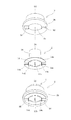
 図1は本発明の実施の形態に係る絶縁アンテナプラグの全体を示す図で、(a)はその正面図、(b)はその側面図、(c)はその背面図である。これらの図に示すように、送信側の同軸ケーブル(図示せず)の終端が接続される入力側(一方)のコネクタ1が絶縁スペーサ2を介して筐体3に固着されるとともに、テレビ受信器等の端末機器側に接続される出力側(他方)のコネクタ4が直接筐体3に固着されている。
 ここで、筐体3は、全体が導電部材で形成された開口部を有する容器である本体5と、本体5の開口部を閉塞する蓋6とからなり、電磁シールドされた密閉空間を形成している。かかる密閉空間である筐体3の内部には、所定の導電路が形成された基板7と、この基板7に実装された所定のコンデンサ8,9とが収納されている。ここで、本体5の側面にはその内部に向けて水平に突出させた凸部10が4箇所に形成してあり、各凸部10に基板7の下面を当接させることにより凸部10を介して筐体3の内部に基板7が載置されている。なお、基板7に関連する他の構成は後に詳述する。
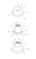
 図2は一方のコネクタ1を抽出して詳細に示す図で、(a)はその正面図、(b)はその背面図、(c)はその側面図である。これらの図に示すように、一方のコネクタ1は同軸ケーブルの内部導体が挿入される孔を有する中心導体11、中心導体11の周囲を取り囲む同心状の絶縁部材12及び絶縁部材12の周囲を空間13を介して取り囲む同心筒状のシールドケース14を有する。本形態においては、中心導体11が一方の内部接続部、またシールドケース14が一方の外部接続部となり、いずれも導電部材で形成されている。同軸ケーブルはその内部導体(銅線)が中心導体11の孔11aに挿入され、またその外部導体(網組み銅線)が絶縁部材12とシールドケース14との間の空間13に挿入されてそれぞれ中心導体11及びシールドケース14に接続されている。
 シールドケース14の基端部はフランジ部14aとなっており、さらにフランジ部14aにおける周方向に関する2箇所にはこのフランジ部14aを切り欠いて切欠部14b、14cを形成し、各切欠部14b、14cから一体的に後方(図2の下方向)に突出させた突出片14d、14eが形成されている。一方、中心導体11にはその基端部が円形の絶縁部材12の中心を貫通して前記後方に突出する同様の突出片11bが形成されている。ここで、突出片11b、14c、14dは中心導体11、絶縁部材12及びシールドケース14が形成する同心円の中心を横断する直線上に位置している。
 図3は絶縁スペーサ2を抽出して詳細に示す図で、(a)はその正面図、(b)はその背面図、(c)はその側面図である。これらの図に示すように、絶縁部材(例えばポリエチレン)で形成した絶縁スペーサ2はコネクタ1を軸方向に貫通させて同軸に保持するための孔2aを有するとともに、その基端部にはフランジ部2bを有する。フランジ部2bの先端側の面(図3(c)の上面)にはその周方向の相対向する2箇所に回り止め用(後に詳述する)の凸部2cが、また基端側の面(図3(c)の下面)にも回り止め用(後に詳述する)の凸部2dがそれぞれ形成されている。
 上述の如きコネクタ1と絶縁スペーサ2とは次のように組み合わせて筐体3に固定する。かかる組立て時の態様を図4及び図5に基づき説明する。両図は何れもコネクタ1と絶縁スペーサ2とを示す斜視図で、図4は筐体3の内部側から見た場合、図5は筐体3の外部側から見た場合をそれぞれ示しており、(a)は絶縁スペーサ2の斜視図、(b)はコネクタ1の斜視図、(c)は組立て斜視図である。これらの図に示すように、コネクタ1は絶縁スペーサ2に形成する孔2aを軸方向に貫通するとともに、シールドケース14の基端部に形成したフランジ部14aが絶縁スペーサ2の基端部に形成したフランジ部2bに当接することによりその軸方向の移動が規制された状態で絶縁スペーサ2に固定されている。ここで、フランジ部2bにおける凸部2dにはフランジ部14aに形成した切欠部14b、14cが嵌入されている。この結果、シールドケース14を介してコネクタ1の絶縁スペーサ2に対する軸周りの回動が規制される。
 かかるコネクタ1及び絶縁スペーサ2は図4(c)及び図5(c)に示すように一体化された状態で筐体3に固定される。筐体3に対する固定は図1及び図6に示すような態様で行われる。
 ここで、図6は図1における筐体3の蓋6を外して示すその内部の平面図である。図1及び図6に示すように、コネクタ1と一体化された絶縁スペーサ2は筐体3に形成する孔5aを筐体3の内部側から貫通するとともに、フランジ部2bを筐体3の内周面に当接させてその軸方向の位置を規制することにより筐体3に固定される。ここで、絶縁スペーサ2のフランジ部2bに形成した凸部2cが筐体3の孔5aに連続する切欠部に嵌入されている。この結果、絶縁スペーサ2の筐体3に対する軸周りの回動が規制される。すなわち、凸部2dでコネクタ1の絶縁スペーサ2に対する軸周りの回動を規制するとともに、凸部2cで絶縁スペーサ2の筐体3に対する軸周りの回動を規制することにより、コネクタ1及び絶縁スペーサ2の軸周りの回動を規制して筐体3に固着している。
 このようにコネクタ1を一体化した絶縁スペーサ2を筐体3に固定することにより、導電体であるフランジ部14aと導電体である筐体3との間に絶縁部材(誘電体)である絶縁スペーサ2のフランジ部2bを挟持することになるので、シールドケース14と筐体3との間に微少容量のコンデンサが形成される。このコンデンサでも雑音を遮断することができる。
 基板7は、前述の如く本体5の側面に形成した凸部10に載置されて筐体3の内部で形成する密閉空間に収納されており、第1の導電部15の途中に第1のコンデンサ8(図中の黒塗り部分)を実装するとともに、第2の導電部16,17間に第2のコンデンサ9(図中の黒塗り部分)を実装してなる。ここで、第1の導電部15,第2の導電部16,17は銅箔で好適に形成することができる。また、本形態における第1の導電部15及び第2の導電部16の一端部にはスリット7a、7b、7cが形成してあり、スリット7aには中心導体11の突出片11bが、スリット7b、7cにはシールドケース14の突出片14d,14eがそれぞれ嵌入される。かくしてスリット7a、7b、7cと突出片11b,14d,14eとの間の隙間を埋めるように半田付けすることにより突出片11bを介してコネクタ1の中心導体11と第1の導電部15とが電気的に接続されるとともに、突出片14d,14eを介してコネクタ1のシールドケース14とが電気的に接続される。ここで、第2の導電部17は半田ランド18を介して半田付けにより筐体3の本体5に電気的に接続される。この結果、シールドケース14は突出片14d,14e、第2の導電部16、第2のコンデンサ9、第2の導電部17及び半田ランド18を介して筐体3に電気的に接続される。なお、本形態において第2のコンデンサ9は4個設けたが,その数に特別な限定はない。少なくとも1個あれば良い。
 他方(出力側)のコネクタ4は、内部接続部である中心導体21及び外部接続部であるシールドケース22が絶縁部材23を介して同心円状に支持されており、本形態ではシールドケース22が直接筐体3に固着してある。また、中心導体21の筐体3側の端部は突出片21aとなって基板7の第1の導電部15の他端部に形成したスリット7dに嵌入されている。かかるスリット7d部分でもスリット7dと突出片21aとの隙間を埋めるように半田付けすることにより中心導体21と第1の導電部15とが電気的に接続される。ここで、本形態においては突出片11b,14d,14eが中心導体11,絶縁部材12及びシールドケース14が形成する同心円の中心を横断する直線上に位置しており、しかも各突出片11b,14d,14eがスリット7a、7b、7cに嵌入されてそれぞれの位置が規制されるので、コネクタ1及び絶縁スペーサ2の筐体3に対する取り付け作業を良好に行うことができる。同様に突出片21aがスリット7dに嵌入されてその位置を規制されるので、コネクタ4の筐体3に対する取り付け作業を良好に行うことができる。
 なお、図6中の灰色部分が半田が乗る部分で第1及び第2の導電部15,16,17の銅箔が露出している部分である。
 図7は本発明の実施の形態に係る絶縁アンテナプラグの等価回路を示す回路図である。同図に示すように、入力側のコネクタ1の中心導体11と出力側のコネクタ4の中心導体21とは途中の第1のコンデンサ8を介して第1の導電部15で接続され,シールドケース14とシールドケース22とは途中の第2のコンデンサ9を介して第2の導電部16,17及び筐体3で接続されている。
 かかる本形態によれば、同軸ケーブルを伝送され中心導体11を介して入力されたメガヘルツ帯域のテレビジョン放送等の高周波数成分は第1のコンデンサ8での減衰が小さいので中心導体21を介してそのまま端末機器側に伝送される。
 一方、同軸ケーブルの内部導体から中心導体11を介して端末機器側に侵入しようとする雑音は第1のコンデンサ8で、また同軸ケーブルの外部導体を介してシールドケース14を介して端末側に侵入しようとする雑音は第2のコンデンサ9でそれぞれ遮断される。
 この結果、端末機器に伝送される信号のS/N比を大きくすることができる。
 また、配電線との混触等により同軸ケーブルの内部導体を介して端末機器側に侵入しようとする商用の高電圧による電流は第1のコンデンサ8で遮断され、同軸ケーブルの外部導体を介して端末側に侵入しようとする商用の高電圧による電流は第2のコンデンサ9で遮断される。
 この結果、かかる高電圧が端末機器に侵入することに伴う不測の不利益を良好に回避することが可能になる。
 なお、本発明は上記実施の形態に限るものではなく、本発明の技術思想の範囲内での任意の変更が可能である。例えば、上記実施の形態では入力側のコネクタ1を絶縁部材である絶縁スペーサ2を介して筐体3に固定したが、これは出力側のコネクタ4を絶縁部材を介して筐体3に固定するようにしても同様の効果が得られる。また、入力側のみならず出力側のコネクタ4も筐体3に対し絶縁した状態で固定しても構わない。
 さらに、本形態では、絶縁スペーサ2のフランジ部2bが筐体3の内側面に当接するように構成したが、図8に示すように、筐体3の孔5aの周囲に筐体3の外周面から前方に突出する導電部材の筒状部材24を設け、この筒状部材24で絶縁スペーサ2の外周面を覆うような構成にすることによりさらに良好な電磁シールドを行うことができる。
 本発明はテレビジョン受信機の製造・販売を行う産業分野において有効に利用することができる。
1       コネクタ
2       絶縁スペーサ
2b      フランジ部
2c、2d   凸部
3       筐体
4       コネクタ
5       本体
5a      孔
7       基板
7a~7d   スリット
8       第1のコンデンサ
9       第2のコンデンサ
10      凸部
11      中心導体
11a     孔
11b     突出片
14      シールドケース
14a     フランジ部
14b     切欠部
14d,14e 突出片
15      第1の導電部
16,17   第2の導電部
21      中心導体
21a     突出片
22      シールドケース
24      筒状部材

Claims (6)

  1.  同軸ケーブルの内部導体が一方の内部接続部に接続されるとともに、前記同軸ケーブルの外部導体が一方の外部接続部に接続され、密閉空間を形成する導電部材の筐体に絶縁部材を介して固定してある一方のコネクタと、
     他方の内部接続部及び他方の外部接続部を介して端末機器のアンテナプラグに接続されるとともに、前記他方の外部接続部が前記筐体に固定してある他方のコネクタと、
     前記一方の内部接続部と前記他方の内部接続部との間に直列に接続されて前記密閉空間内に配設されている第1のコンデンサと、
     前記一方の外部接続部と前記筐体との間に接続されて前記密閉空間内に配設されている第2のコンデンサとを有することを特徴とする絶縁アンテナプラグ。
  2.  請求項1に記載する絶縁アンテナプラグにおいて、
     前記一方のコネクタの一方の内部接続部に一端が接続されるとともに、前記他方のコネクタの他方の内部接続部に他端が接続された第1の導電部を有する基板を前記密閉空間内に配設するとともに、
     前記第1のコンデンサを前記第1の導電部の途中で前記基板上に実装し、
     さらに前記第2のコンデンサを前記基板に形成された第2の導電部を介して前記基板上に実装したことを特徴とする絶縁アンテナプラグ。
  3.  請求項1に記載する絶縁アンテナプラグにおいて、
     前記絶縁部材は前記筐体に形成する孔を前記筐体の内部側から貫通するとともに、その基端部に形成するフランジ部を前記筐体の内周面に当接させてその軸方向の位置を規制することにより前記筐体に固定し、
     前記一方のコネクタは前記絶縁部材に形成する孔を軸方向に貫通するとともに、その一方の外部接続部の基端部に形成したフランジ部が前記絶縁部材の前記フランジ部に当接することによりその軸方向の移動が規制された状態で前記絶縁部材を介して前記筐体に固定したことを特徴とする絶縁アンテナプラグ。
  4.  請求項2に記載する絶縁アンテナプラグにおいて、
     前記絶縁部材は前記筐体に形成する孔を前記筐体の内部側から貫通するとともに、その基端部に形成するフランジ部を前記筐体の内周面に当接させてその軸方向の位置を規制することにより前記筐体に固定し、
     前記一方のコネクタは前記絶縁部材に形成する孔を軸方向に貫通するとともに、その一方の外部接続部の基端部に形成したフランジ部が前記絶縁部材の前記フランジ部に当接することによりその軸方向の移動が規制された状態で前記絶縁部材を介して前記筐体に固定したことを特徴とする絶縁アンテナプラグ。
  5.  請求項2乃至請求項4の何れか一つに記載する絶縁アンテナプラグにおいて、
     前記一方のコネクタの前記一方の内部接続部及び前記一方の外部接続部は前記筐体の内部に突出する一体的な突出片をそれぞれ有するとともに、
     前記基板の前記第1及び第2の導電部の一部には前記突出片がそれぞれ嵌入されるスリットを有することを特徴とする絶縁アンテナプラグ。
  6.  請求項3又は請求項4に記載する絶縁アンテナプラグにおいて、
     前記絶縁部材のフランジ部における前記一方の外部接続部のフランジ部の当接面側及びその反対面側にそれぞれ凸部を形成する一方、
     前記一方の外部接続部のフランジ部には前記当接面側の凸部に嵌入されて前記一方のコネクタの軸周りの回動を規制する切欠き部を形成するとともに、
     前記筐体の前記孔には前記反対面側の凸部が嵌入されて前記絶縁部材の軸周りの回動を規制する切欠き部を形成したことを特徴とする絶縁アンテナプラグ。
PCT/JP2009/059902 2009-05-29 2009-05-29 絶縁アンテナプラグ Ceased WO2009128567A1 (ja)

Priority Applications (2)

Application Number Priority Date Filing Date Title
CN2009800001815A CN101682159B (zh) 2009-05-29 2009-05-29 绝缘天线插头
PCT/JP2009/059902 WO2009128567A1 (ja) 2009-05-29 2009-05-29 絶縁アンテナプラグ

Applications Claiming Priority (1)

Application Number Priority Date Filing Date Title
PCT/JP2009/059902 WO2009128567A1 (ja) 2009-05-29 2009-05-29 絶縁アンテナプラグ

Publications (1)

Publication Number Publication Date
WO2009128567A1 true WO2009128567A1 (ja) 2009-10-22

Family

ID=41199246

Family Applications (1)

Application Number Title Priority Date Filing Date
PCT/JP2009/059902 Ceased WO2009128567A1 (ja) 2009-05-29 2009-05-29 絶縁アンテナプラグ

Country Status (2)

Country Link
CN (1) CN101682159B (ja)
WO (1) WO2009128567A1 (ja)

Cited By (2)

* Cited by examiner, † Cited by third party
Publication number Priority date Publication date Assignee Title
WO2016104586A1 (ja) * 2014-12-26 2016-06-30 日本電業工作株式会社 同軸ケーブル接続部材、通信回路及び通信装置
JP2016127008A (ja) * 2014-12-26 2016-07-11 日本電業工作株式会社 同軸ケーブル接続部材、通信回路及び通信装置

Families Citing this family (3)

* Cited by examiner, † Cited by third party
Publication number Priority date Publication date Assignee Title
KR101119170B1 (ko) * 2010-05-10 2012-03-20 최동욱 알에프 동축 커넥터의 결합손실 절감회로
KR101477399B1 (ko) * 2013-06-28 2014-12-29 삼성전기주식회사 알에프 모듈
KR101588708B1 (ko) * 2014-09-02 2016-01-28 주식회사 솔루엠 알에프 모듈

Citations (11)

* Cited by examiner, † Cited by third party
Publication number Priority date Publication date Assignee Title
JPS4968317U (ja) * 1972-09-30 1974-06-14
JPS49101293U (ja) * 1972-12-20 1974-08-31
JPS50125094U (ja) * 1974-03-28 1975-10-14
JPS55135376U (ja) * 1979-03-19 1980-09-26
JPS582877U (ja) * 1981-06-30 1983-01-10 八木アンテナ株式会社 同軸接栓座
JPS6217965A (ja) * 1985-07-16 1987-01-26 マスプロ電工株式会社 高周波機器の信号入出力装置
JPS6225484U (ja) * 1985-07-30 1987-02-16
JPH0320886U (ja) * 1989-07-11 1991-02-28
JPH0561908U (ja) * 1991-11-27 1993-08-13 株式会社小糸製作所 車両用灯具のコネクタ保持構造
JP2005268148A (ja) * 2004-03-22 2005-09-29 M & M Kk 伝送線介設型濾波器
JP2009105008A (ja) * 2007-10-25 2009-05-14 Kojima Press Co Ltd 同軸ケーブルと回路基板の接続構造

Family Cites Families (2)

* Cited by examiner, † Cited by third party
Publication number Priority date Publication date Assignee Title
CN2678207Y (zh) * 2003-10-22 2005-02-09 世同电子股份有限公司 射频转接装置
CN201167187Y (zh) * 2007-12-19 2008-12-17 王光华 一种能滤除数码声的转换插头

Patent Citations (11)

* Cited by examiner, † Cited by third party
Publication number Priority date Publication date Assignee Title
JPS4968317U (ja) * 1972-09-30 1974-06-14
JPS49101293U (ja) * 1972-12-20 1974-08-31
JPS50125094U (ja) * 1974-03-28 1975-10-14
JPS55135376U (ja) * 1979-03-19 1980-09-26
JPS582877U (ja) * 1981-06-30 1983-01-10 八木アンテナ株式会社 同軸接栓座
JPS6217965A (ja) * 1985-07-16 1987-01-26 マスプロ電工株式会社 高周波機器の信号入出力装置
JPS6225484U (ja) * 1985-07-30 1987-02-16
JPH0320886U (ja) * 1989-07-11 1991-02-28
JPH0561908U (ja) * 1991-11-27 1993-08-13 株式会社小糸製作所 車両用灯具のコネクタ保持構造
JP2005268148A (ja) * 2004-03-22 2005-09-29 M & M Kk 伝送線介設型濾波器
JP2009105008A (ja) * 2007-10-25 2009-05-14 Kojima Press Co Ltd 同軸ケーブルと回路基板の接続構造

Cited By (2)

* Cited by examiner, † Cited by third party
Publication number Priority date Publication date Assignee Title
WO2016104586A1 (ja) * 2014-12-26 2016-06-30 日本電業工作株式会社 同軸ケーブル接続部材、通信回路及び通信装置
JP2016127008A (ja) * 2014-12-26 2016-07-11 日本電業工作株式会社 同軸ケーブル接続部材、通信回路及び通信装置

Also Published As

Publication number Publication date
CN101682159A (zh) 2010-03-24
CN101682159B (zh) 2012-01-04

Similar Documents

Publication Publication Date Title
JP3045726B1 (ja) アンテナ線接続用l型コネクタ
KR101829077B1 (ko) Rf 간섭 억제기
JP5221188B2 (ja) シールドコネクタ
US20050148227A1 (en) Microphone output connector
WO2009128567A1 (ja) 絶縁アンテナプラグ
JP2004022199A (ja) プラグ付き同軸ケーブル
JP2005203217A (ja) シールドコネクタ
JP4560380B2 (ja) コンデンサマイクロホンの出力コネクタ
KR20050113620A (ko) 안테나 장치 및 안테나 장치의 제조 방법
JP6933382B2 (ja) 同軸コネクタ、高周波ユニット及び受信装置
JP4770665B2 (ja) アンテナ装置
JPH06215648A (ja) 同軸ケーブル
JP7570089B2 (ja) 車両用アンテナ装置
JPH1174037A (ja) 多芯電気コネクタケーブル組立体
JP2006174310A (ja) コンデンサーマイクロホン
JP3558852B2 (ja) コンピュータ用チューナボード及びその製造方法
US12206151B2 (en) Coaxial isolator
US20240332870A1 (en) Connector, connector system and transmission method
JP6782810B2 (ja) 同軸ケーブルコネクタ
JP2928102B2 (ja) 同軸コネクター
KR970006762B1 (ko) 안테나 시일드 박스
JP2902333B2 (ja) 同軸プラグ
JP3062286U (ja) シ―ルド形プラグ付ケ―ブル
JP2019145216A (ja) 同軸ケーブル用プラグ
JP2021021861A (ja) 電子機器

Legal Events

Date Code Title Description
WWE Wipo information: entry into national phase

Ref document number: 200980000181.5

Country of ref document: CN

121 Ep: the epo has been informed by wipo that ep was designated in this application

Ref document number: 09731767

Country of ref document: EP

Kind code of ref document: A1

NENP Non-entry into the national phase

Ref country code: DE

122 Ep: pct application non-entry in european phase

Ref document number: 09731767

Country of ref document: EP

Kind code of ref document: A1

NENP Non-entry into the national phase

Ref country code: JP