WO2009095951A1 - プラズマディスプレイパネル - Google Patents
プラズマディスプレイパネル Download PDFInfo
- Publication number
- WO2009095951A1 WO2009095951A1 PCT/JP2008/000110 JP2008000110W WO2009095951A1 WO 2009095951 A1 WO2009095951 A1 WO 2009095951A1 JP 2008000110 W JP2008000110 W JP 2008000110W WO 2009095951 A1 WO2009095951 A1 WO 2009095951A1
- Authority
- WO
- WIPO (PCT)
- Prior art keywords
- electrode
- scan
- discharge
- display panel
- address
- Prior art date
- Legal status (The legal status is an assumption and is not a legal conclusion. Google has not performed a legal analysis and makes no representation as to the accuracy of the status listed.)
- Ceased
Links
Images




Classifications
-
- H—ELECTRICITY
- H01—ELECTRIC ELEMENTS
- H01J—ELECTRIC DISCHARGE TUBES OR DISCHARGE LAMPS
- H01J11/00—Gas-filled discharge tubes with alternating current induction of the discharge, e.g. alternating current plasma display panels [AC-PDP]; Gas-filled discharge tubes without any main electrode inside the vessel; Gas-filled discharge tubes with at least one main electrode outside the vessel
- H01J11/20—Constructional details
- H01J11/34—Vessels, containers or parts thereof, e.g. substrates
- H01J11/36—Spacers, barriers, ribs, partitions or the like
-
- H—ELECTRICITY
- H01—ELECTRIC ELEMENTS
- H01J—ELECTRIC DISCHARGE TUBES OR DISCHARGE LAMPS
- H01J11/00—Gas-filled discharge tubes with alternating current induction of the discharge, e.g. alternating current plasma display panels [AC-PDP]; Gas-filled discharge tubes without any main electrode inside the vessel; Gas-filled discharge tubes with at least one main electrode outside the vessel
- H01J11/10—AC-PDPs with at least one main electrode being out of contact with the plasma
- H01J11/12—AC-PDPs with at least one main electrode being out of contact with the plasma with main electrodes provided on both sides of the discharge space
-
- H—ELECTRICITY
- H01—ELECTRIC ELEMENTS
- H01J—ELECTRIC DISCHARGE TUBES OR DISCHARGE LAMPS
- H01J11/00—Gas-filled discharge tubes with alternating current induction of the discharge, e.g. alternating current plasma display panels [AC-PDP]; Gas-filled discharge tubes without any main electrode inside the vessel; Gas-filled discharge tubes with at least one main electrode outside the vessel
- H01J11/20—Constructional details
- H01J11/22—Electrodes, e.g. special shape, material or configuration
- H01J11/26—Address electrodes
-
- H—ELECTRICITY
- H01—ELECTRIC ELEMENTS
- H01J—ELECTRIC DISCHARGE TUBES OR DISCHARGE LAMPS
- H01J2211/00—Plasma display panels with alternate current induction of the discharge, e.g. AC-PDPs
- H01J2211/20—Constructional details
- H01J2211/22—Electrodes
- H01J2211/26—Address electrodes
- H01J2211/265—Shape, e.g. cross section or pattern
-
- H—ELECTRICITY
- H01—ELECTRIC ELEMENTS
- H01J—ELECTRIC DISCHARGE TUBES OR DISCHARGE LAMPS
- H01J2211/00—Plasma display panels with alternate current induction of the discharge, e.g. AC-PDPs
- H01J2211/20—Constructional details
- H01J2211/34—Vessels, containers or parts thereof, e.g. substrates
- H01J2211/36—Spacers, barriers, ribs, partitions or the like
- H01J2211/361—Spacers, barriers, ribs, partitions or the like characterized by the shape
Definitions
- the present invention relates to a plasma display panel having a discharge gap formed by electrodes extending in the same direction.
- the plasma display panel has a gas filled space sandwiched between a pair of substrates, and performs color display by selectively emitting red, green and blue ultraviolet-excited phosphors by gas discharge.
- the display discharge for causing the phosphor to emit light is a so-called surface discharge type discharge (hereinafter referred to as a surface discharge).
- the surface discharge is generated in an electrode gap (surface discharge gap) between the sustain electrode and the scan sustain electrode extending in parallel along the horizontal direction of the matrix display region (hereinafter referred to as a screen).
- the sustain electrodes and the scan sustain electrodes define display lines corresponding to the rows of the matrix display in the screen.
- Address electrodes are arranged on the screen so as to intersect the display lines, and cells serving as display elements respectively correspond to the intersections between the display lines and the address electrodes.
- Fig. 1 shows the basic cell structure of a plasma display panel.
- the front plate 10z and the back plate 20z are drawn separately for easy understanding of the internal structure.
- the plasma display panel 9 is composed of a front plate 10z, a back plate 20z facing the front plate 10z, and a discharge gas (not shown) sealed in a facing gap between the front plate 10z and the back plate 20z.
- the front plate 10 z includes a glass substrate 11, sustain electrodes Xz and scan sustain electrodes Yz arranged in parallel to the glass substrate 11, sustain electrodes Xz, and scan sustain electrodes Yz.
- the insulator layer 16 is a laminate of a dielectric layer 17 and a protective film 18 that prevents sputtering.
- the protective film 18 is generally made of magnesium oxide.
- the back plate 20z includes a plurality of partitions arranged in correspondence between the glass substrate 21, the address electrodes Az arranged on the glass substrate 21 at equal intervals, the dielectric layer 22 covering the address electrodes Az, and the address electrodes Az. 24z, a red (R) phosphor 26, a green (G) phosphor 27, and a blue (B) phosphor 28.
- the partition wall pattern of the plasma display panel 9 is a strike type pattern that partitions the gas filled space for each column of the matrix display. That is, each partition 24z is a vertical wall extending in the vertical direction of the screen, and the plasma display panel 9 does not have a horizontal wall extending in the horizontal direction.
- the lattice pattern that partitions the gas-filled space for each cell is becoming the mainstream instead of the strike type pattern.
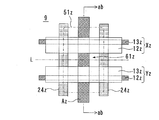
- FIG. 2 shows the positional relationship between the three electrodes and the barrier ribs in one cell 51z of the plasma display panel 9 of FIG.
- the sustain electrode Xz and the scan sustain electrode Yz that define the display line L are each composed of a strip-shaped transparent conductor 12 and a metal strip 13 that is thinner than the transparent conductor 12.
- the transparent conductor 12 of the sustain electrode Xz and the transparent conductor 12 of the scan sustain electrode Yz form a surface discharge gap 61z in the cell 51z.
- the address electrode Az extending across the surface discharge gap 61z intersects the sustain electrode Xz and the scan sustain electrode Yz in the middle of the adjacent partition wall 24z.
- the scan sustaining electrode Yz is used as a scanning electrode for sequentially selecting the display line L
- the address electrode Az is used as a data electrode for giving display data to the selected display line.
- an address discharge 71z occurs between the selected scan sustain electrode Yz and the selected address electrode Az.
- the type of the address discharge 71z is called a counter discharge type because it is a discharge between the mutually facing surfaces of the scan sustaining electrode Yz and the address electrode Az.
- the sustain electrode Xz and the scan sustain electrode Yz are used to apply an alternating polarity voltage to the surface discharge gap 61z.
- a display discharge 72z is generated between the sustain electrode Xz and the scan sustain electrode Yz as shown in FIG. 3B in a cell in which a predetermined amount of wall charges remains.
- the display discharge 72z is a surface discharge.
- Japanese Patent Application Laid-Open No. 2001-222959 which is a prior art document, discloses an electrode arrangement shown in FIG. 4, elements corresponding to those in FIG. 2 are denoted by the same reference numerals.
- the address electrode Azb of the plasma display panel 9b shown in FIG. 4 has a thin strip portion 81 that overlaps the partition wall 24z and a protruding portion 82 that protrudes from the strip portion 81 toward the partition gap.
- the protruding portion 82 partially overlaps the scan sustaining electrode Yz and partially corresponds to the surface discharge gap 61z. However, the protruding portion 82 does not overlap the sustain electrode Xz. In the configuration of FIG.
- the region where the counter discharge between the address electrode Azb and the scan sustaining electrode Yz occurs can be limited to the region where the protruding portion 82 is disposed, thereby reducing the discharge current and the fluorescent light emitting surface. It is possible to reduce the area that deteriorates due to the counter discharge at. JP 2001-222959 A
- the present invention has been made in view of such circumstances, and an object of the present invention is to provide a plasma display panel that is useful for reducing a change over time in which display disturbance becomes remarkable.
- a plasma display panel that achieves the above object includes a first substrate and a second substrate sandwiching a gas filled space, a plurality of sustain electrodes and a plurality of scan sustain electrodes arranged in parallel to the first substrate to define display lines for matrix display An insulating layer covering the sustain electrodes and the scan sustain electrodes, a plurality of address electrodes arranged on the second substrate and intersecting the sustain electrodes and the scan sustain electrodes, and disposed corresponding to the address electrodes. A plurality of vertical walls are provided to partition the gas enclosure space.
- each of the plurality of intersecting portions that overlap each of the address electrodes in the scan sustaining electrode includes a non-discharge region portion that overlaps one of the vertical walls and a counter discharge region portion that does not overlap the vertical wall.
- the counter discharge region portion of the scan sustain electrode is a part of the edge of the scan sustain electrode and corresponds to the display line. It is away from the surface discharge gap part that forms the surface discharge gap together with the sustain electrode.
- the counter discharge region portion in each scan sustain electrode is separated from the surface discharge gap portion in the scan sustain electrode, that is, the counter discharge region portion does not include the surface discharge gap portion, the counter discharge region portion of the insulator layer
- the ion bombardment by the surface discharge between the sustain electrode and the scan sustain electrode with respect to the portion covering the surface is smaller than the ion bombardment in the case where the counter discharge region portion includes the surface discharge gap portion. It is desirable that the distance between the counter discharge region portion and the surface discharge gap portion is larger within a range that does not hinder the formation of wall charges in a portion close to the surface discharge gap in the insulator layer.
- the vertical wall is formed in a strip shape in which the width of at least a portion of the portion overlapping the scan sustain electrode is smaller than the width of the portion of the address electrode overlapping the scan sustain electrode, and the address electrode and the portion Are arranged so as to overlap each other.
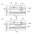
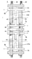
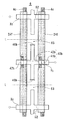
- FIG. 3 is a diagram showing a cross-sectional structure corresponding to the ab-ab arrow of FIG. 2 in a basic cell configuration. It is a figure which shows the modification of the shape and arrangement
- FIG. 6 is a diagram showing cross-sectional structures corresponding to the 6a-6a arrow view, 6b-6b arrow view, 6c-6c arrow view, and 6d-6d arrow view of FIG.
- the plasma display panel according to the embodiment of the present invention basically has the same configuration as the known plasma display panel 9 shown in FIG. 1 except for the arrangement of the address electrodes and the shape of the vertical wall.
- the plasma display panels 1 to 6 exemplified below are composed of a front plate and a back plate which are stacked so as to sandwich a gas filled space and whose peripheral portions are joined together, and a discharge gas filled in the gas filled space. It has a square display matrix display area (hereinafter referred to as a screen) of a predetermined size capable of color display. 5 to 11 referred to in the following description, elements denoted by the same reference numerals as those in FIGS. 1 to 3 correspond to the elements shown in FIGS. In the following, description of these elements is omitted or simplified.
- the plasma display panel 1 includes a sustain electrode X and a scan sustain electrode Y that define a display line L for matrix display, a plurality of address electrodes A that intersect with the sustain electrode X and the plurality of scan sustain electrodes Y, and an address electrode A.
- a plurality of vertical walls 24 that are arranged in correspondence with each other and define a gas filled space.
- the illustrated sustain electrode X is one of a plurality of sustain electrodes X arranged on a first substrate which is a glass substrate of a front plate
- the scan sustain electrode Y is a plurality of scan sustain electrodes arranged on the first substrate.
- Each of the sustain electrodes X and the scan sustain electrodes Y includes a transparent conductor 12 and a metal strip 13.
- the address electrodes A are arranged on a second substrate that is a glass substrate of the back plate.
- the characteristics of the plasma display panel 1 apparent from the comparison between FIG. 5 and FIG. 2 are that the vertical walls 24 are arranged so as to overlap the address electrodes A and extend in the vertical direction of the screen, and are locally formed in a thin strip shape. It is that.
- a thin portion of the vertical wall 24 is a portion 241 of the scan sustaining electrode Y that intersects the metal band 13, and its width W1 is a width of other portions including only a portion of the scan sustaining electrode Y that overlaps only the transparent conductor 12. It is smaller than W2 and smaller than the width W5 of the address electrode A.
- the intersection 40 overlapping the address electrode A in the scan sustain electrode Y is adjacent to the vertical line.
- a non-discharge region 41 that overlaps one of the walls 24 and a counter discharge region 42 that does not overlap the vertical wall 24 are provided.
- the counter discharge region portion 42 of the scan sustain electrode Y is separated from the surface discharge gap portion 45 that is a part of the edge of the scan sustain electrode Y.
- the surface discharge gap portion 45 is a portion that forms the surface discharge gap 61 together with one sustain electrode X corresponding to the display line L including the cell 51.
- the gas discharge space 31 corresponding to the cell 51 includes a first region for generating an address discharge 71 of a counter discharge type, and a surface discharge type of discharge. This is divided into a second region for generating the display discharge 72. That is, a first region dedicated to the address discharge 71 and a second region dedicated to the display discharge 72 are formed in one gas discharge space 31. However, since the first region and the second region are not physically separated, it is possible to move the space charge that produces a priming effect between these regions.
- the first region for generating the address discharge 71 is a region corresponding to the counter discharge region 42 of the scan sustaining electrode Y. And the position of this 1st area
- region is a position shifted in the direction along the display line L with respect to the surface discharge gap 61 of the cell 51, as FIG. 5 shows. Accordingly, the first region is substantially isolated from the ion flow accompanying the display discharge 71 in the surface discharge gap 61.
- the portion related to the address discharge 71 in the protective film 18 on the dielectric layer 17 does not receive the ion bombardment due to the display discharge 71 or is slight even if received, so the structure as shown in FIG.
- the progress of the deterioration of the protective film 18 causing the increase in the discharge delay of the address discharge 71 is slow. That is, in the plasma display panel 1, the addressing reliability can be maintained over a cumulative display time longer than the conventional one.
- the plasma display panel 2 includes a sustain electrode Xb, a scan sustain electrode Yb, an address electrode Ab, and a grid-like partition wall 23.
- Each display line L is determined by a pair of the sustain electrode Xb and the scan sustain electrode Yb, and each of the regions defined by the partition walls 23 corresponds to a cell.
- the sustain electrodes Xb and the scan sustain electrodes Yb arranged on the first substrate are each composed of an energizing portion extending along the display line L and a plurality of projecting portions projecting from the energizing portion toward the surface discharge gap 62 for each cell.
- the protruding portion can be a transparent conductor and the energizing portion can be a metal band alone or a laminate of a metal band and a transparent conductor.
- the configuration of the sustain electrode Xb and the scan sustain electrode Yb is arbitrary.
- the address electrode Ab arranged on the second substrate is formed in a locally thick band shape that intersects with the scan sustaining electrode Y. Since it is locally thick, the area of the region facing the scan sustaining electrode Y is sufficiently large to cause address discharge.
- the partition wall 23 includes a plurality of vertical walls 24b that determine both ends of the cell in the horizontal direction and a plurality of horizontal walls 25 that determine both ends of the cell in the vertical direction.
- the vertical wall 24b has a locally thin shape at a portion intersecting with the scan sustaining electrode Yb in plan view.
- the gas discharge space corresponding to each cell includes a first region for generating an address discharge and a first region for generating a display discharge. It is divided into two areas.
- the plasma display panel 3 includes a sustain electrode Xb, a scan sustain electrode Yb, an address electrode Ab, and a grid-like partition wall 23b.
- the partition wall 23 b includes a plurality of vertical walls 24 c and a plurality of horizontal walls 25.
- the vertical wall 24c has a locally thick band shape at a portion between the intersection position with the scan sustaining electrode Yb and the display line L close thereto in plan view.
- the position of the counter discharge region 44 of the scan sustaining electrode Yb is shifted in the direction along the display line L with respect to the surface discharge gap 62.
- the gas discharge space corresponding to is divided into a first region for generating an address discharge and a second region for generating a display discharge.
- the plasma display panel 4 includes a sustain electrode Xb, a scan sustain electrode Yb, an address electrode Ab, and a grid-like partition wall 23c.
- the partition wall 23c includes a plurality of vertical walls 24d and a plurality of horizontal walls 25.
- the vertical wall 24d has a thin band shape in which the portion intersecting with the scan sustaining electrode Yb and the portion intersecting with the sustaining electrode Xb are locally thin in a plan view.
- the position of the counter discharge region 44 of the scan sustaining electrode Yb is shifted in the direction along the display line L with respect to the surface discharge gap 62, and the gas discharge space corresponding to each cell performs address discharge.
- a first region for generating a discharge and a second region for generating a display discharge are divided.
- the gas discharge space of each cell has a symmetrical shape with the display line L as the center line, the discharge with the sustain electrode Xb as the anode and the scan maintenance are repeated during the display discharge by applying the alternating polarity voltage.
- the discharge conditions are equivalent between the discharge using the electrode Yb as the anode. This is preferable in terms of display stability.
- the plasma display panel 5 includes a sustain electrode Xb, a scan sustain electrode Yb, an address electrode Ab, and a grid-like partition wall 23d.
- the partition wall 23d includes a plurality of vertical walls 24e and a plurality of horizontal walls 25.
- the plasma display panel 5 is characterized by an electrode arrangement in which the scan sustain electrodes Yb defining the odd display lines L and the scan sustain electrodes Yb defining the even display lines L are adjacent to each other. It is.
- the sustain electrodes Xb that define the odd-numbered display lines L are adjacent to the sustain electrodes Yb that define the even-numbered display lines L.
- the position of the counter discharge region 44 of the scan sustaining electrode Yb is shifted in the direction along the display line L with respect to the surface discharge gap 62, and the gas discharge space corresponding to each cell performs address discharge.
- a first region for generating the image and a second region for generating a display discharge are divided.
- the plasma display panel 6 includes a sustain electrode Xc, a scan sustain electrode Yc, an address electrode Ac, and a plurality of vertical walls 24f.
- Each display line L is determined by a pair of the sustain electrode Xc and the scan sustain electrode Yc, and one cell 52 corresponds to each display line L in a band-shaped region determined by the adjacent partition wall 24f.
- the sustain electrodes Xc and the scan sustain electrodes Yc that are alternately arranged on the first substrate at equal intervals extend from the energization portion and the surface discharge gap 63 on both sides of the energization portion and the cell for each cell extending along the display line L.
- Each of the plurality of protruding portions protrudes.
- the scan sustaining electrode Yc is involved in the display of two adjacent display lines L. The same applies to the sustain electrode Xc.
- the address electrode Ac arranged on the second substrate is formed in a locally thick band shape that intersects with the scan sustaining electrode Yc. Since it is locally thick, the area of the region facing the scan sustaining electrode Yc is sufficiently large to cause address discharge.
- the vertical walls 24f are arranged so as to overlap the address electrodes Ac and extend in the vertical direction of the screen, and the portions intersecting with the scanning sustain electrodes Yc in a plan view have a locally narrow band shape.
- the width of the narrow portion of the vertical wall 24f is smaller than the width of the thick portion of the address electrode Ac.
- the intersection 40b of the scan sustain electrode Yc overlapping the address electrode Ac overlaps with one of the adjacent vertical walls 24f. It has a counter discharge region portion 42b that does not overlap the discharge region portion 41b and the vertical wall 24f.
- the counter discharge region 42b of the scan sustain electrode Yc is a part of the edge of the scan sustain electrode Yc and forms a surface discharge gap 63 together with the sustain electrode X corresponding to the cell. It is away from 46b.
- the position of the counter discharge region portion 42b of the scan sustaining electrode Yc is shifted in the direction along the display line L with respect to the surface discharge gap 63, and the gas discharge space corresponding to each cell 52 is address discharge.
- the gas discharge space corresponding to each cell 52 is address discharge.
- the present invention contributes to the improvement of the life of the plasma display panel.
Landscapes
- Engineering & Computer Science (AREA)
- Physics & Mathematics (AREA)
- Plasma & Fusion (AREA)
- Chemical & Material Sciences (AREA)
- Materials Engineering (AREA)
- Gas-Filled Discharge Tubes (AREA)
Abstract
アドレス放電にかかわる絶縁体層の劣化の進行が遅いプラズマディスプレイパネル(1)は、非放電領域部(41)および対向放電領域部(42)を有した走査維持電極(Y)を備える。非放電領域部(41)は走査維持電極(Y)におけるアドレス電極(A)と重なる複数の交差部分(40)の一部分であって、複数の垂直壁(24)のうちの1つと重なる。対向放電領域部(42)は交差部分(40)の他の一部分であって、垂直壁(24)と重ならない。対向放電領域部(42)は当該走査維持電極(Y)の端縁のうちの面放電ギャップ(61)を形成する面放電ギャップ部(45)から離れている。
Description
本発明は、同一方向に延びる電極によって形成される放電ギャップを有したプラズマディスプレイパネルに関する。
プラズマディスプレイパネルは、基板対に挟まれたガス封入空間をもち、ガス放電によって赤、緑および青の3色の紫外線励起型蛍光体を選択的に発光させてカラー表示を行う。蛍光体を発光させる表示放電は、いわゆる面放電形式の放電(以下、これを面放電という)である。面放電はマトリクス表示領域(以下、画面という)の水平方向に沿って平行に延びる維持電極と走査維持電極との電極間隙(面放電ギャップ)で生じる。維持電極および走査維持電極はマトリクス表示の行にそれぞれ対応する表示ラインを画面内に定める。画面には表示ラインと交差するようにアドレス電極が配列され、表示ラインとアドレス電極との交点に表示素子であるセルがそれぞれ対応する。
図1はプラズマディスプレイパネルの基本的なセル構造を示す。同図では内部構造を分かり易くするために前面板10zと背面板20zとを分離させて描いてある。
図1のように、プラズマディスプレイパネル9は前面板10z、前面板10zと対向する背面板20z、および前面板10zと背面板20zとの対向間隙に封入された図示しない放電ガスから構成される。前面板10zは、ガラス基板11、ガラス基板11に平行に配列された維持電極Xzおよび走査維持電極Yz、維持電極Xzおよび走査維持電極Yzを被覆する絶縁体層16を有する。絶縁体層16は誘電体層17とスパッタリングを防ぐ保護膜18の積層である。保護膜18は一般に酸化マグネシウムからなる。背面板20zは、ガラス基板21、ガラス基板21上に等間隔に配列されたアドレス電極Az、アドレス電極Azを覆う誘電体層22、アドレス電極Azの電極間に対応付けて配置された複数の隔壁24z、赤(R)の蛍光体26、緑(G)の蛍光体27、および青(B)の蛍光体28を備える。
プラズマディスプレイパネル9の隔壁パターンは、マトリクス表示の列ごとにガス封入空間を区画するストタイプパターンである。すなわち、各隔壁24zは画面の垂直方向に延びる垂直壁であり、プラズマディスプレイパネル9は水平方向に延びる水平壁を有していない。ただし、近年ではセルごとにガス封入空間を区画する格子パターンがストタイプパターンに代わって主流になりつつある。
図2は図1のプラズマディスプレイパネル9の1つのセル51zにおける3つの電極と隔壁との配置関係を示す。表示ラインLを定める維持電極Xzおよび走査維持電極Yzはそれぞれ帯状の透明導体12と透明導体12よりも細い金属帯13とからなる。維持電極Xzの透明導体12と走査維持電極Yzの透明導体12とがセル51z内に面放電ギャップ61zを形成する。この面放電ギャップ61zを横切るように延びるアドレス電極Azは、隣接する隔壁24zの中間で維持電極Xzおよび走査維持電極Yzと交差する。
このようなプラズマディスプレイパネル9による表示においては、画面内のセル51zの誘電体の壁電荷量を表示データに対応づけるアドレッシングと、壁電荷を利用してセルを選択的に発光させるサステインとが行なわれる。
アドレッシングにおいて、走査維持電極Yzが表示ラインLを順に選択するための走査電極として用いられ、アドレス電極Azが選択表示ラインに表示データを与えるデータ電極として用いられる。図3(A)のように、選択された走査維持電極Yzと選択されたアドレス電極Azとの間でアドレス放電71zが起こる。アドレス放電71zの形式は、走査維持電極Yzおよびアドレス電極Azの互いの対向面どうしの間の放電であることから、対向放電形式と呼ばれる。
サステインにおいては、維持電極Xzおよび走査維持電極Yzが面放電ギャップ61zへの交番極性電圧の印加に用いられる。交番極性電圧の印加によって、所定量の壁電荷が残存するセルにおいて、図3(B)のように維持電極Xzと走査維持電極Yzとの間で表示放電72zが起こる。表示放電72zは面放電である。
アドレス電極Azの変形に関して、先行技術文献である特開2001-222959号公報は図4に示す電極配置を開示している。図4において図2に対応する要素には同一の符号を付してある。図4が示すプラズマディスプレイパネル9bのアドレス電極Azbは隔壁24zと重なる細い帯状部分81とこの帯状部分81から隔壁間隙へ向かって張り出した突起部分82とを有する。突起部分82は走査維持電極Yzと部分的に重なり、かつ面放電ギャップ61zにも部分的に対応する。しかし、突起部分82は維持電極Xzとは重ならない。図4の構成では、アドレス電極Azbと走査維持電極Yzとの間の対向放電が起こる領域を突起部分82の配置された領域に限定することができ、それにより放電電流を低減しかつ蛍光発光面における対向放電で劣化する領域を減少させることができる。
特開2001-222959号公報
プラズマディスプレイパネルの累積表示時間が長くなるにつれてアドレス放電ミスの発生確率が徐々に大きくなる。アドレス放電ミスは表示の乱れとして現れる。図3(A)および(B)によく示されるように、従来のプラズマディスプレイパネル9では、保護膜18のうちのアドレス放電71zによるイオン衝撃を強く受ける部分、すなわち走査維持電極Yzとアドレス電極Azとの対向領域に対応した部分180が、表示放電72zによるイオン衝撃をも受ける。表示放電72zのエネルギーはアドレス放電71zのエネルギーよりも大きく、通常の表示における単位時間当たりのアドレス放電71zの回数よりも表示放電72zの回数は多い。また、保護膜18の膜質が放電遅れに深く関わることが知られている。これらのことから、アドレス放電ミスが起こり易くなる経時変化は、保護膜18のうちのアドレス放電71zに関与する部分180が主として表示放電72zによって劣化するので起こる現象であると推察される。図4の構成についても同様である。
アドレッシングが高速であるほど印加パルスのパルス幅が短くアドレス放電ミスがより起こり易い。解像度および輝度を高めるには、アドレス放電ミスを起こり難くしてより高速のアドレッシングを行う必要がある。
本発明は、このような事情に鑑みてなされたものであり、表示の乱れが顕著になる経時変化の低減に有用なプラズマディスプレイパネルの提供を目的としている。
上記目的を達成するプラズマディスプレイパネルは、ガス封入空間を挟む第1基板および第2基板、前記第1基板に平行に配列されてマトリクス表示の表示ラインを定める複数の維持電極および複数の走査維持電極、前記維持電極および走査維持電極を被覆する絶縁体層、前記第2基板に配列されて前記維持電極および走査維持電極と交差する複数のアドレス電極、および前記アドレス電極に対応づけて配置されて前記ガス封入空間を区画する複数の垂直壁を備える。当該プラズマディスプレイパネルにおいては、前記走査維持電極における前記アドレス電極のそれぞれと重なる複数の交差部分のそれぞれが、前記垂直壁の1つと重なる非放電領域部および前記垂直壁と重ならない対向放電領域部を有している。そして、前記表示ラインのそれぞれに対応する1本の走査維持電極において、当該走査維持電極の対向放電領域部が、当該走査維持電極の端縁の一部分であって当該表示ラインに対応する1本の維持電極と一緒に面放電ギャップを形成する面放電ギャップ部から離れている。
各走査維持電極における対向放電領域部が当該走査維持電極における面放電ギャップ部と離れているので、すなわち対向放電領域部が面放電ギャップ部を含まないので、絶縁体層のうちの対向放電領域部を覆う部分に対する維持電極と走査維持電極との間の面放電によるイオン衝撃は、対向放電領域部が面放電ギャップ部を含む場合のイオン衝撃よりも小さい。対向放電領域部と面放電ギャップ部との距離は、絶縁体層における面放電ギャップに近い部分への壁電荷形成に支障のない範囲内でより大きいのが望ましい。
好ましい態様において、前記垂直壁は、前記走査維持電極と重なる部分の少なくとも一部分の幅が、前記アドレス電極における前記走査維持電極と重なる部分の幅よりも小さい帯状に形成され、かつ前記アドレス電極と部分的に重なるように配置される。
本発明の実施形態に係るプラズマディスプレイパネルは、アドレス電極の配置および垂直壁の形状を除いて基本的には図1に示した公知のプラズマディスプレイパネル9と同様の構成をもつ。以下に例示されるプラズマディスプレイパネル1~6は、ガス封入空間を挟むように重ねられて周縁部どうしが接合された前面板と背面板、およびガス封入空間に充填された放電ガスから構成され、カラー表示の可能な所定サイズの正方配列のマトリクス表示領域(以下、画面という)を有する。以下の説明で参照する図5~図11において、図1~図3と同一の符号が付された要素は図1~図3に示される要素に対応した要素である。以下ではこれら要素の説明は省略されまたは簡略化される。
図5において、プラズマディスプレイパネル1は、マトリクス表示の表示ラインLを定める維持電極Xおよび走査維持電極Y、維持電極Xおよび複数の走査維持電極Yと交差する複数のアドレス電極A、およびアドレス電極Aのそれぞれに対応づけて配置されてガス封入空間を区画する複数の垂直壁24を備える。図示された維持電極Xは前面板のガラス基板である第1基板に配列された複数の維持電極Xの1つであり、同様に走査維持電極Yは第1基板に配列された複数の走査維持電極Yの1つである。維持電極Xおよび走査維持電極Yはそれぞれが透明導体12と金属帯13とからなる。アドレス電極Aは背面板のガラス基板である第2基板に配列されている。
図5と図2との比較で明らかなプラズマディスプレイパネル1の特徴は、垂直壁24がアドレス電極Aにそれぞれ重なって画面の垂直方向に延びるように配置され、かつ局部的に細い帯状に形成されていることである。垂直壁24における細い部分は走査維持電極Yのうちの金属帯13と交差する部分241であり、その幅W1は走査維持電極Yのうちの透明導体12のみと重なる部分を含む他の部分の幅W2よりも小さくかつアドレス電極Aの幅W5よりも小さい。この特徴を有することから、任意の1つのセル51に対応した1つの走査維持電極Yおよび1つのアドレス電極Aに注目すると、走査維持電極Yにおけるアドレス電極Aと重なる交差部分40が、隣接する垂直壁24の一方と重なる非放電領域部41および垂直壁24と重ならない対向放電領域部42を有している。そして、当該走査維持電極Yの対向放電領域部42が、当該走査維持電極Yの端縁の一部分である面放電ギャップ部45から離れている。面放電ギャップ部45はセル51を含む表示ラインLに対応した1本の維持電極Xと一緒に面放電ギャップ61を形成する部分である。
図6(A)~(D)を参照すると明らかなように、セル51に対応するガス放電空間31は、対向放電形式のアドレス放電71を生じさせるための第1の領域と、面放電形式の表示放電72を生じさせるための第2の領域とに区分される。つまり、1つのガス放電空間31の中にアドレス放電71に専用の第1の領域と表示放電72に専用の第2の領域とが形成される。ただし、第1の領域と第2の領域とは物理的に隔てられてはいないので、これら領域の間でプライミング効果を生む空間電荷の移動は可能である。
アドレス放電71を生じさせるための第1の領域は走査維持電極Yの対向放電領域部42に対応した領域である。そして、この第1の領域の位置は、図5が示すとおり、セル51の面放電ギャップ61に対して表示ラインLに沿う方向にずれた位置である。したがって、第1の領域は、面放電ギャップ61での表示放電71に伴うイオン流に対して実質的に隔離される。
プラズマディスプレイパネル1においては、誘電体層17上の保護膜18におけるアドレス放電71に関与する部分が表示放電71によるイオン衝撃を受けないかまたは受けても軽微であるので、図1のような構造をもつ従来のプラズマディスプレイパネルと比べて、アドレス放電71の放電遅れの増大を招く保護膜18の劣化の進行が遅い。すなわち、プラズマディスプレイパネル1では、従来よりも長い累積表示時間にわたってアドレッシングの信頼性を保つことができる。
以下に、プラズマディスプレイパネル1の変形例を挙げる。
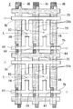
図7において、プラズマディスプレイパネル2は、維持電極Xb、走査維持電極Yb、アドレス電極Ab、および格子状の隔壁23を備える。各表示ラインLは維持電極Xbと走査維持電極Ybとの対によって定まり、隔壁23で区画される領域のそれぞれがセルに対応する。
第1基板に配列される維持電極Xbおよび走査維持電極Ybは、それぞれが表示ラインLに沿って延びる通電部と、セルごとに通電部から面放電ギャップ62へ向かって突き出る複数の突出部とからなる。突出部を透明導体としかつ通電部を金属帯のみまたは金属帯と透明導体との積層とすることができる。また、通電部および突出部を金属で形成してもよい。本発明の目的を達成する電極パターンを有する限り、維持電極Xbおよび走査維持電極Ybの構成は任意である。
第2基板に配列されるアドレス電極Abは、走査維持電極Yと交差する部分が局部的に太い帯状に形成されている。局部的に太いので、走査維持電極Yと対向する領域の面積はアドレス放電を生じさせる上で十分に大きい。
隔壁23は、セルの水平方向の両端を決める複数の垂直壁24bと、セルの垂直方向の両端を決める複数の水平壁25とで構成される。垂直壁24bは平面視において走査維持電極Ybと交差する部分が局部的に細い形状をもつ。
任意の1つのセルに対応した1つの走査維持電極Ybおよび1つのアドレス電極Abに注目すると、走査維持電極Ybにおけるアドレス電極Abと重なる交差部分が、垂直壁24bおよび水平壁25のどちらとも重ならない対向放電領域部44を有している。そして、この対向放電領域部44が当該走査維持電極Ybの面放電ギャップ部46から離れている。対向放電領域部44の位置は、面放電ギャップ62に対して表示ラインLに沿う方向にずれた位置である。したがって、上述のプラズマディスプレイパネル1と同様に、プラズマディスプレイパネル2においても、各セルに対応するガス放電空間は、アドレス放電を生じさせるための第1の領域と、表示放電を生じさせるための第2の領域とに区分される。
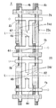
図8において、プラズマディスプレイパネル3は、維持電極Xb、走査維持電極Yb、アドレス電極Ab、および格子状の隔壁23bを備える。隔壁23bは、複数の垂直壁24cと複数の水平壁25とで構成される。垂直壁24cは平面視において走査維持電極Ybとの交差位置とそれに近い表示ラインLとの間の部分が局部的に太い帯形状をもつ。プラズマディスプレイパネル3においても、上述のプラズマディスプレイパネル1と同様に、走査維持電極Ybの対向放電領域部44の位置は面放電ギャップ62に対して表示ラインLに沿う方向にずれており、各セルに対応するガス放電空間はアドレス放電を生じさせるための第1の領域と表示放電を生じさせるための第2の領域とに区分される。
図9において、プラズマディスプレイパネル4は、維持電極Xb、走査維持電極Yb、アドレス電極Ab、および格子状の隔壁23cを備える。隔壁23cは、複数の垂直壁24dと複数の水平壁25とで構成される。垂直壁24dは平面視において走査維持電極Ybと交差する部分および維持電極Xbと交差する部分が局部的に細い帯形状をもつ。プラズマディスプレイパネル4においても、走査維持電極Ybの対向放電領域部44の位置は面放電ギャップ62に対して表示ラインLに沿う方向にずれており、各セルに対応するガス放電空間はアドレス放電を生じさせるための第1の領域と表示放電を生じさせるための第2の領域とに区分される。
プラズマディスプレイパネル4では、各セルのガス放電空間が表示ラインLを中心線とする対称形状であるので、交番極性電圧の印加による表示放電の繰り返しにおいて、維持電極Xbを陽極とする放電と走査維持電極Ybを陽極とする放電との間で放電条件が同等である。このことは表示の安定の上で好ましい。
図10において、プラズマディスプレイパネル5は、維持電極Xb、走査維持電極Yb、アドレス電極Ab、および格子状の隔壁23dを備える。隔壁23dは、複数の垂直壁24eと複数の水平壁25とで構成される。プラズマディスプレイパネル5の特徴は、図7との対比で明らかなように、奇数番目の表示ラインLを定める走査維持電極Ybと偶数番目の表示ラインLを定める走査維持電極Ybとが隣り合う電極配列である。図では示されないが、奇数番目の表示ラインLを定める維持電極Xbは偶数番目の表示ラインLを定める維持電極Ybと隣り合う。プラズマディスプレイパネル5においても、走査維持電極Ybの対向放電領域部44の位置は面放電ギャップ62に対して表示ラインLに沿う方向にずれており、各セルに対応するガス放電空間はアドレス放電を生じさせるための第1の領域と表示放電を生じさせるための第2の領域とに区分される。
図11において、プラズマディスプレイパネル6は、維持電極Xc、走査維持電極Yc、アドレス電極Ac、および複数の垂直壁24fを備える。各表示ラインLは維持電極Xcと走査維持電極Ycとの対によって定まり、隣接する隔壁24fで定まる帯状領域において表示ラインLのそれぞれに1つのセル52が対応する。
第1基板に交互に等間隔に配列される維持電極Xcおよび走査維持電極Ycは、それぞれが表示ラインLに沿って延びる通電部とセルごとに通電部からその両側の面放電ギャップ63へ向かってそれぞれ突き出る複数の突出部とからなる。図示のとおり、走査維持電極Ycは隣接する2本の表示ラインLの表示に関わる。維持電極Xcも同様である。
第2基板に配列されるアドレス電極Acは、走査維持電極Ycと交差する部分が局部的に太い帯状に形成されている。局部的に太いので、走査維持電極Ycと対向する領域の面積はアドレス放電を生じさせる上で十分に大きい。
垂直壁24fはアドレス電極Acにそれぞれ重なって画面の垂直方向に延びるように配置され、平面視において走査維持電極Ycと交差する部分が局部的に細い帯形状をもつ。垂直壁24fにおける細い部分の幅は、アドレス電極Acの太い部分の幅よりも小さい。
任意の1つのセル52に対応する1つの走査維持電極Ycおよび1つのアドレス電極Acに注目すると、走査維持電極Ycにおけるアドレス電極Acと重なる交差部分40bが、隣接する垂直壁24fの一方と重なる非放電領域部41bおよび垂直壁24fと重ならない対向放電領域部42bを有している。そして、当該走査維持電極Ycの対向放電領域部42bが、当該走査維持電極Ycの端縁の一部分であって当該セルに対応した維持電極Xと一緒に面放電ギャップ63を形成する面放電ギャップ部46bから離れている。
プラズマディスプレイパネル6においても、走査維持電極Ycの対向放電領域部42bの位置は面放電ギャップ63に対して表示ラインLに沿う方向にずれており、各セル52に対応するガス放電空間はアドレス放電を生じさせるための第1の領域と表示放電を生じさせるための第2の領域とに区分される。
本発明は、プラズマディスプレイパネルの寿命の向上に貢献する。
Claims (3)
- ガス封入空間を挟む第1基板および第2基板、前記第1基板に平行に配列されてマトリクス表示の表示ラインを定める複数の維持電極および複数の走査維持電極、前記維持電極および走査維持電極を被覆する絶縁体層、前記第2基板に配列されて前記維持電極および走査維持電極と交差する複数のアドレス電極、および前記アドレス電極に対応づけて配置されて前記ガス封入空間を区画する複数の垂直壁を備えたプラズマディスプレイパネルであって、
前記走査維持電極における前記アドレス電極のそれぞれと重なる複数の交差部分のそれぞれが、前記垂直壁の1つと重なる非放電領域部および前記垂直壁と重ならない対向放電領域部を有しており、
前記表示ラインのそれぞれに対応する1本の走査維持電極において、当該走査維持電極の対向放電領域部が、当該走査維持電極の端縁の一部分であって当該表示ラインに対応する1本の維持電極と一緒に面放電ギャップを形成する面放電ギャップ部から離れている
ことを特徴とするプラズマディスプレイパネル。 - 前記垂直壁は、前記走査維持電極と重なる部分の少なくとも一部分の幅が、前記アドレス電極における前記走査維持電極と重なる部分の幅よりも小さい帯状に形成され、かつ前記アドレス電極と部分的に重なるように配置された
請求項1に記載のプラズマディスプレイパネル。 - 前記垂直壁は、マトリクス表示の表示素子ごとに前記ガス封入空間を区画する格子状の隔壁の一部分である
請求項2に記載のプラズマディスプレイパネル。
Priority Applications (1)
| Application Number | Priority Date | Filing Date | Title |
|---|---|---|---|
| PCT/JP2008/000110 WO2009095951A1 (ja) | 2008-01-30 | 2008-01-30 | プラズマディスプレイパネル |
Applications Claiming Priority (1)
| Application Number | Priority Date | Filing Date | Title |
|---|---|---|---|
| PCT/JP2008/000110 WO2009095951A1 (ja) | 2008-01-30 | 2008-01-30 | プラズマディスプレイパネル |
Publications (1)
| Publication Number | Publication Date |
|---|---|
| WO2009095951A1 true WO2009095951A1 (ja) | 2009-08-06 |
Family
ID=40912325
Family Applications (1)
| Application Number | Title | Priority Date | Filing Date |
|---|---|---|---|
| PCT/JP2008/000110 Ceased WO2009095951A1 (ja) | 2008-01-30 | 2008-01-30 | プラズマディスプレイパネル |
Country Status (1)
| Country | Link |
|---|---|
| WO (1) | WO2009095951A1 (ja) |
Citations (1)
| Publication number | Priority date | Publication date | Assignee | Title |
|---|---|---|---|---|
| JP2001015036A (ja) * | 1999-06-29 | 2001-01-19 | Fujitsu Ltd | プラズマディスプレイパネル |
-
2008
- 2008-01-30 WO PCT/JP2008/000110 patent/WO2009095951A1/ja not_active Ceased
Patent Citations (1)
| Publication number | Priority date | Publication date | Assignee | Title |
|---|---|---|---|---|
| JP2001015036A (ja) * | 1999-06-29 | 2001-01-19 | Fujitsu Ltd | プラズマディスプレイパネル |
Similar Documents
| Publication | Publication Date | Title |
|---|---|---|
| EP1684322B1 (en) | Plasma display panel | |
| JP3960813B2 (ja) | プラズマディスプレイパネル | |
| WO2009095951A1 (ja) | プラズマディスプレイパネル | |
| JP4894234B2 (ja) | プラズマディスプレイパネル | |
| JP3641386B2 (ja) | プラズマディスプレイパネル | |
| US7701414B2 (en) | Plasma display panel and method of driving the same | |
| KR100757027B1 (ko) | 플라즈마 디스플레이 패널 | |
| JP2008027608A (ja) | プラズマディスプレイパネル | |
| JP4788304B2 (ja) | プラズマディスプレイパネル | |
| JP4436291B2 (ja) | プラズマディスプレイパネル | |
| JP4962323B2 (ja) | プラズマディスプレイパネル | |
| JP2007141483A (ja) | プラズマディスプレイパネル | |
| JP2006228639A (ja) | プラズマディスプレイパネル | |
| JP4465339B2 (ja) | 単色表示に適したプラズマディスプレイ装置 | |
| KR100637168B1 (ko) | 플라즈마 디스플레이 패널 | |
| US20090309495A1 (en) | Plasma display panel | |
| US20070152595A1 (en) | Plasma display panel | |
| KR100669379B1 (ko) | 플라즈마 디스플레이 패널 | |
| JP2007005048A (ja) | プラズマディスプレイパネル | |
| JP2006059631A (ja) | プラズマディスプレイパネル | |
| JP2006344577A (ja) | プラズマディスプレイ装置 | |
| KR20090075527A (ko) | 플라즈마 디스플레이 패널 | |
| JP2004355840A (ja) | プラズマディスプレイパネル | |
| JP2006324033A (ja) | プラズマディスプレイパネル | |
| JP2007311130A (ja) | プラズマディスプレイパネル |
Legal Events
| Date | Code | Title | Description |
|---|---|---|---|
| 121 | Ep: the epo has been informed by wipo that ep was designated in this application |
Ref document number: 08702842 Country of ref document: EP Kind code of ref document: A1 |
|
| NENP | Non-entry into the national phase |
Ref country code: DE |
|
| 122 | Ep: pct application non-entry in european phase |
Ref document number: 08702842 Country of ref document: EP Kind code of ref document: A1 |
|
| NENP | Non-entry into the national phase |
Ref country code: JP |