WO2006095489A1 - 誤りバイト数を制限したバイト内複数スポッティバイト誤り訂正・検出方法及び装置 - Google Patents
誤りバイト数を制限したバイト内複数スポッティバイト誤り訂正・検出方法及び装置 Download PDFInfo
- Publication number
- WO2006095489A1 WO2006095489A1 PCT/JP2005/023545 JP2005023545W WO2006095489A1 WO 2006095489 A1 WO2006095489 A1 WO 2006095489A1 JP 2005023545 W JP2005023545 W JP 2005023545W WO 2006095489 A1 WO2006095489 A1 WO 2006095489A1
- Authority
- WO
- WIPO (PCT)
- Prior art keywords
- error
- byte
- matrix
- bytes
- bit
- Prior art date
- Legal status (The legal status is an assumption and is not a legal conclusion. Google has not performed a legal analysis and makes no representation as to the accuracy of the status listed.)
- Ceased
Links
Classifications
-
- H—ELECTRICITY
- H03—ELECTRONIC CIRCUITRY
- H03M—CODING; DECODING; CODE CONVERSION IN GENERAL
- H03M13/00—Coding, decoding or code conversion, for error detection or error correction; Coding theory basic assumptions; Coding bounds; Error probability evaluation methods; Channel models; Simulation or testing of codes
- H03M13/03—Error detection or forward error correction by redundancy in data representation, i.e. code words containing more digits than the source words
- H03M13/05—Error detection or forward error correction by redundancy in data representation, i.e. code words containing more digits than the source words using block codes, i.e. a predetermined number of check bits joined to a predetermined number of information bits
- H03M13/13—Linear codes
-
- G—PHYSICS
- G06—COMPUTING OR CALCULATING; COUNTING
- G06F—ELECTRIC DIGITAL DATA PROCESSING
- G06F11/00—Error detection; Error correction; Monitoring
- G06F11/07—Responding to the occurrence of a fault, e.g. fault tolerance
- G06F11/08—Error detection or correction by redundancy in data representation, e.g. by using checking codes
- G06F11/10—Adding special bits or symbols to the coded information, e.g. parity check, casting out 9's or 11's
-
- G—PHYSICS
- G06—COMPUTING OR CALCULATING; COUNTING
- G06F—ELECTRIC DIGITAL DATA PROCESSING
- G06F11/00—Error detection; Error correction; Monitoring
-
- G—PHYSICS
- G06—COMPUTING OR CALCULATING; COUNTING
- G06F—ELECTRIC DIGITAL DATA PROCESSING
- G06F12/00—Accessing, addressing or allocating within memory systems or architectures
- G06F12/16—Protection against loss of memory contents
-
- H—ELECTRICITY
- H03—ELECTRONIC CIRCUITRY
- H03M—CODING; DECODING; CODE CONVERSION IN GENERAL
- H03M13/00—Coding, decoding or code conversion, for error detection or error correction; Coding theory basic assumptions; Coding bounds; Error probability evaluation methods; Channel models; Simulation or testing of codes
- H03M13/03—Error detection or forward error correction by redundancy in data representation, i.e. code words containing more digits than the source words
- H03M13/05—Error detection or forward error correction by redundancy in data representation, i.e. code words containing more digits than the source words using block codes, i.e. a predetermined number of check bits joined to a predetermined number of information bits
- H03M13/13—Linear codes
- H03M13/15—Cyclic codes, i.e. cyclic shifts of codewords produce other codewords, e.g. codes defined by a generator polynomial, Bose-Chaudhuri-Hocquenghem [BCH] codes
Definitions
- the present invention relates to a spotty byte light error correction 'detection method and apparatus. More specifically, the present invention relates to a word consisting of a plurality of bits as a byte field and a word (word) composed of the plurality of bytes.
- An error that causes multiple spotty byte errors within one byte is called ⁇ multi-spotty byte error within a byte '', and when multiple spotty byte errors within that byte occur in a limited number of bytes, Multiple spotty byte error correction within a byte with a limited number of error bytes, which is suitable for detecting or correcting the error, that is, “multiple spotty byte errors within a byte with a limited number of error bytes”. 'Relates to a detection method and apparatus. Background art
- codes that correct 1-byte errors and detect 2-byte errors are read solo codes (Reed-Solomon codes). It has been proposed as an improved and efficient code, and has already been adopted in main storage devices such as many computer systems (for example, see Non-Patent Document 3 and Non-Patent Document 4).
- Non-Patent Document 6 gives a comprehensive overview of many of the interrelated code research and development related to the late 1980s.
- Non-Patent Document 7 also describes a code that corrects a 1-byte error and detects a simultaneous error of 1-bit error and 1-byte error (S b EC — (S + S b ) ED code Is proposed in Non-Patent Document 8 ing.
- Non-Patent Document 9 discloses a code that corrects a 1-byte error and corrects it if there is a 2-bit error (referred to as S b EC-DEC code). .
- an error up to t bit (tb) in a byte consisting of b bits is called a tb error or a spotty byte error.
- S t / b EC code for correcting bets errors, and to correct the 1 Supottibai bets errors, and about the S t / b EC _ S b ED code detecting one byte error exceeding bytes in t bit The invention has already been disclosed (see Patent Document 1).
- the St / b EC code is disclosed in Non-Patent Document 10.
- DRAM elements semiconductor memory elements
- a temporary failure has occurred due to noise, alpha particles, or the like.
- a fixed failure may occur in which the DRAM device itself deteriorates and becomes inoperable.
- More than 80% of devices using recent DRAM elements are said to be temporary failures.
- DRAM elements having multi-bit data input / output of 8 bits or more are 1 in bytes. A relatively small number of bit errors, such as a few bits, are the majority.
- the S t / b EC- S b ED code that can be configured to give an arbitrary value for the parameter t and b, 8-bit This is a very practical encoding method when used in a memory device that uses DRAM elements equal to or higher than the above.
- RS code Red Solomon code
- the S t / b EC- D t / b ED _ S b ED code the DR AM element above 8-bit This is a very practical encoding method when used in the memory device used.
- the S t / b EC- D t / b ED _ S b ED code is correct the child and is capable of functioning an error of 1 element of up to small t-bit Installing by carbonochloridate I-wide b ( 1 spotty byte error correction, St / b EC), a function that can detect spotty byte errors across 2 elements (2 spotty errors) Byte error detection, D t / b ED), and a function that can detect a 1-byte error that exceeds t bits although the probability of occurrence is small (1 bit error detection, S b ED), which corrects bit errors with a significantly smaller number of check bits compared to the conventional coding method in units of bytes.
- the present invention has been made in view of the circumstances as described above, and an object of the present invention is to control multiple spotty byte errors in multiple bytes generated in a limited number of bytes. It is an object of the present invention to provide an intra-byte multiple spotty byte error correction / detection method and apparatus having a function capable of performing error correction and limiting the number of error bytes.
- Another object of the present invention is to detect a single-by-h error that has a small probability of occurrence but exceeds the correction capability of multiple spotty notch errors within the symbol. It is an object of the present invention to provide a multi-spot spot byte error correction / detection method and apparatus having a function to limit the number of error bytes. Disclosure of the invention
- the present invention provides encoding means for generating a transmission word based on input information data and decoding means for correcting or detecting the error by inputting the transmission in which an error has occurred in an information transmission path as a reception word.
- the present invention has the above-mentioned object of the present invention to provide a parity check matrix that expresses a spotty-byte error control code and a parity check matrix that expresses a spotty-byte error control code.
- Syndrome generating means for generating a received word syndrome, and an error correction for correcting or detecting the five received errors based on the syndrome generated by the syndrome generating means.
- the input information data is composed of a plurality of bytes
- the input information data is composed of a plurality of bytes. It is assumed that the errors up to the bit (up to bit) are called spotty byte errors, and the error that causes multiple spotty spot errors within one byte is called multiple spotty spot errors within a byte.
- the Supottibai preparative error control code represented by the parity check matrix occurs i number of by-Bok number of correct the Ri erroneous Supottibai preparative and occurring number of by-Bok;!
- the information Transmission path is a information communication system this Alternatively, the information transmission path is effectively a memory system, or alternatively, the information transmission path is a bus line circuit.
- the parity check matrix corrects Ai i spotty byte errors occurring in pi bytes and occurs in p 2 bytes; U 2 spotty bytes Used for the multi-spotty byte error control code (/ only EC-[ 2 ⁇ bED 2 code) within the byte with the error detection function and limited number of error bytes.
- H r ° H " ⁇ 2 ⁇ " ⁇ r 2i H n- .. "r ° H” .., + Pi-,) i H ". .. Pl + ft- 1 )
- the matrix H 'is H' [ho ' , H 1 ', ⁇ ' ⁇ , h b —] is a binary matrix of q rows b ⁇ IJ (q ⁇ b) composed of q-order column vectors (0 ⁇ j ⁇ b-1) If ( ⁇ ! + 2 ) t or b is less than or smaller than t or b, the matrix H 'is the unit when ( ⁇ ! + ⁇ 2 ) t ⁇ b.
- the parity check matrix is generated in p bytes; correction of spotty byte errors and ⁇ 2 spotty byte errors occurring in p 2 bytes.
- used for the multi-spotted-byte error control code (decompression [/ bEC-[ ⁇ 2 ⁇ bED] p2 code) within the decompression byte with the number of error bytes limited.
- a matrix, + 2 ) / 2 ”columns that are less than or equal to t or b are linearly independent, where
- the matrix H '' is a regular matrix including a unit matrix
- parity check matrix of the code with t + 1, ie, Lo, + 2 ) / 2 ”t-bit error detection function (b, b — r)
- the parity check matrix is generated in pi bytes; u is corrected in ⁇ ⁇ spotty byte errors, and p 2 is generated in 2 bytes. Limits the number of error bytes, with the ability to detect one spot byte error and detect one byte error that exceeds the correction capability. Multiple spotted byte error control codes (
- the parity check matrix corrects the number of spotty byte errors occurring in p bytes and includes ⁇ 2 spotty bytes occurring in p 2 bytes. Limits the number of error bytes with the ability to detect errors and detect single-byte errors that exceed the correction capability.
- R -th order column vector hj (0 ⁇ j ⁇ b-1), which is an r-by-b binary matrix (r ⁇ b), whichever is smaller than t or b
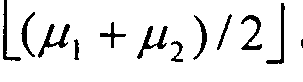
- [] represents the largest integer not exceeding X, where [(/, + // 2 ) / 2 ”t ⁇
- the matrix H is a regular matrix including an identity matrix, and when LC", +) / 2 "t ⁇ b, the matrix H" is the minimum nominal distance + / 1 ⁇ 2) / 2 ”parity check matrix of code with t + 1, that is, parity check matrix of (b, b _ r) code with L (A + ⁇ 2 ) / 2” t bit error detection function
- ⁇ is the primitive element of r 'next extension field GF (2 r ') of GF (2) and y W-I ⁇ i Cho ") ⁇ ' ⁇ (h 1 "), ...
- the above-described object of the present invention is to provide an intra-byte multiple spotty byte error control code ([ ⁇ , ⁇ / bEC] ⁇ ⁇ [// bED] p2 code) in which the number of error bytes is limited. If the value is set to 1 (t 1), ⁇ ⁇ random bit errors that occur in pi bytes are corrected and ⁇ 2 bytes occur; u 2 random bit errors Or a random bit error control code with a limited number of error bytes, or a plurality of spotty byte error control codes in an extended byte with a limited number of error bytes. (Expansion [/ bEC,-[/ bED] P2 code), when the t value is set to 1
- the above-described object of the present invention is that when the parity check matrix (H) is t ⁇ b / 1 ( ⁇ , +, the matrix ⁇ 'and the matrix ⁇ "are linearly independent of arbitrary b columns.
- the parity check matrix (H) is t ⁇ b Z [(// , + 2) / 2 "and the when, the matrix H 'and the matrix H” is any column b linearly independent matrix and Do Ri, Ri by the the child matches the pi bytes when correcting errors and monitor p 2 by the secondary has a feature at detecting an error extension RS code parity check matrix, or the parity check matrix (H), when set to t ⁇ b / [( ⁇ + / 2) / 2 ", the matrix Eta” is Ri Do any b columns linearly independent matrix, Ba By the the child matches the RS code parity check matrix having a With correct bets error and function to detect the monitor P 2 bytes error Ri, Or, the parity check matrix (H) is , T ⁇
- the error correction means generates a bit error pointer that detects which bit of the received word is incorrect based on the syndrome, and generates the bit error pointer. Based on the bit error pointer, the error of the received word is corrected by inverting the bit value of the received word corresponding to the error bit, and the bit of the received word is corrected.
- the error correction means outputs an uncorrectable error detection signal, or the error correction means includes an H ′ decoding means, an H ”multiplication means, and a GF ( 2 r ) parallel decoding means, GF (2 b ) error generation means, and inversion Five
- the H ′ decoding means is configured to detect an error for each byte based on the upper q bits of the syndrome generated by the syndrome generation means. generates a sum (e. a), the H "multiplication means, based on the sum (e a) of errors for each of the bytes that play generated by the H 'decoding means, the error of each of the byte
- the product of the transposed matrix of the sum (e A ) and H ′′ is generated, and the parallel decoding means on the GF (2 r ) calculates the sum of errors for each byte generated by the H ”multiplication means (e A bit on GF ( 2r ) based on the product of the transposed matrix of A ) and H "and the remaining lower bits excluding the upper q bits of the syndrome generated by the syndrome generation means mis Ri pointer, and was considered impossible error correction in a parallel decoding on GF (2 r) Generating a first uncorrectable error detection signal outputted to come, the error generation means on the GF (2 b), the H
- the above-mentioned object of the present invention is that the error generating means on the GF (2 b ) is a decoding result obtained from the 1 noise force of the bit error pointer (e ′) on the GF (2 r ).
- the bit error pointer () outputs a detection signal for 1 byte and i byte of t bit error correction decoding means, and outputs only the number of input detection signal weights for the i bytes.
- a multi-input sorting means for outputting the 1 from the upper bits continuous to, miscorrection determined conducted, i by outputting a 1-byte of the GF (2 b) on the bit error pointer (e)
- an error generation means on the GF ( 2b ) includes a t-bit error correction decoding means, a multi-input sorting means, and an i-by-bit sorting means. And t-bit error correction decoding means.
- the detection signal in i byte ⁇ ⁇ which is a signal for detecting an error exceeding the correction capability is sent to the multi-input sorting means and the i
- the multi-input sorting means counts the weights (number of 1s) of detection signals in the plurality of i-bytes that are input, and outputs only the number of the weights.
- the error correction judging means for the i byte is the means for continuously outputting 1 from the upper bits of the output, and the decoding result output from the t bit error correction decoding means for all bytes.
- Bit error pointer ( ⁇ ) Wherein i detection signal in bytes, and then with the byte input a sum of your capital error (e A), performs erroneous correction determining, the GF (2 b) on the bit error pointer (e ) Or the error generation means on the GF ( 2b ) is the second most significant bit in the signal output from the multi-input sorting means.
- the GF (2) which is output as the second uncorrectable error detection signal and which collects the signals output from the error correction judging means in the i byte and has the number of bits of code bit length. b ) Effectively achieved by outputting the above bit error pointer.
- the above-mentioned object of the present invention is to provide the error correction determination means in the i byte, wherein the error correction determination is performed by the following error correction determination formula:
- the [/ 6EC] p, - [ / bED] p2 - S a ED marks Nos, and the elongation, - [/ bED] 1 ⁇ 2 - For S 6 ED code, S before Symbol H "multiplication means When a syndrome other than! Is newly input, and S!
- a detection signal is output, and is added to the error generation means on the GF (2 b ).
- the error generation means on GF (2 b ) checks whether the number of error bytes at error e ′ on GF (2 r ) is 1 or not. This is achieved effectively by configuring the decoding means by checking whether the Hamming weight using the first means is larger than ⁇ it.
- the present invention provides an encoding process step for generating a transmission word based on input information data, and correcting or detecting the error by inputting the transmission word in which an error has occurred in an information transmission path as a reception word. And a decryption process step 8
- the above-described object of the present invention is to provide a parity check matrix representing a spotty byte error control code and a parity check matrix.
- the transmission information is generated by adding the check information generated based on the input information data to the input information data, and the decoding step includes the parity check matrix.
- a syndrome generation processing step for generating a syndrome of the received word based on the error, and an error correction for correcting or outputting the error of the received word based on the syndrome generated by the syndrome generation processing step
- the input information data consists of a plurality of bytes, where b (b is an integer greater than or equal to 2) is 1 byte
- An error up to t bits (l ⁇ t ⁇ b) in a byte is called a spotty error, and an error in which multiple spotty byte errors occur in one byte is a multiple spotty byte in the byte.
- the spotty-byte error control code represented by the parity check matrix corrects i spotty-byte errors occurring in pj bytes, and p 2 U 2 spotty byte errors are detected, and the t value, b value, p, value, p 2 value, ⁇ i value, and 2 value are set arbitrarily, where pj ⁇ p 2 And i ⁇ 2 are established, and the information transmission path is effectively achieved by being an information communication system, a memory system, or a bus line circuit.
- the above-described object of the present invention is that the error correction processing step generates a bit error pointer that detects which bit of the received word is incorrect based on the syndrome. Based on the bit error pointer, the received word error is corrected by inverting the bit value of the received word corresponding to the error bit, and the bit error of the received word is corrected. With correction 9
- the error correction processing step includes an H ′ decoding processing step, an H ”multiplication processing step, and a GF ( 2 r ), a parallel decoding processing step on GF (2 b ), an inversion processing step, and an inversion processing step.
- the H ′ decoding processing step includes An error sum (e A ) for each byte is generated based on the upper q bits of the syndrome generated in the dream generation processing step
- the H ”multiplication processing step includes H, based on the sum (e a) of errors for each of the bytes generated by the decoding process stearyl-up, the product of the transposed matrix of the sum of errors for each of the bytes (e a) and H " generated, parallel decoding processing step in the on the GF (2 r), the front H upper q bits of the thin palindrome that product, and generated by the thin palindrome generation processing scan Tetsupu transposed matrix of "error sum of each of the bytes that are generated by the multiplication processing step (e A) and H" based on the remaining lower bits except, GF (2 r) on the bit error pointer, and GF (2 r) impossible error correction in a parallel decoding on.
- the first uncorrectable error detection signal is generated, and the error generation processing step on the GF ( 2b ) is the error for each byte generated in the H ′ decoding processing step. sum (e a), and, based on the bit error pointer on the GF (2 r) said generated by the parallel decoding processing steps on GF (2 r), bit on GF (2 b) Error pointer, and the second correction that is output when error correction is deemed impossible Impossible to generate an error detection signal, the S rolling process stearyl-up is a bit error pointers of said on GF (2 b) on the GF generated by the error generation process stearyl-up (2 b) On the basis of this, by correcting the error of the received word by inverting the bit value of the received word corresponding to the bit error pointer on the GF ( 2b ).
- the first uncorrectable error detection signal generated in the parallel decoding processing step on the GF ( 2r ) and the GF ( 2b ) A third that indicates that an error exceeding the correction capability has been detected by taking the logical sum of the second uncorrectable error detection signal generated in the error generation processing step above. This is effectively achieved by outputting a non-correctable error detection signal.
- the above-described object of the present invention is that the error generation processing step on the GF (2 b ) is performed by decoding from one byte of the bit error pointer (e ′) on the GF (2 r ).
- a t-bit error correction decoding process step for outputting a detection signal at 1 and i nodes of a bit error pointer (), and detection signals of a plurality of input i bytes.
- the error generation processing step on the GF (2) includes a t-bit error correction decoding processing step and a multi-bit error correction decoding processing step.
- the detection signal at i-byte which is a signal, is output to the multi-input sort processing step and the error correction determination processing step at the i-byte, and the multi-input sort processing step includes a plurality of input i Count the weight of the detected signal (number of 1s) in the buy ⁇ , and only the number of weights is the higher order bits of the output. 2 to 1 are output in succession, and the error correction determination processing step for the i byte includes the decoding result bit error pointer (from the t bit error correction decoding processing step for all bytes).
- the detection signal in the i byte and the sum of errors for each byte (e A ) are input, and an error correction determination is performed, and the bit error pointer (e) on the GF (2 b ) is determined.
- the error generation processing step on the GF ( 2b ) the higher 2 bits of the signal output from the multi-input sorting processing step are output.
- the second signal is output as the second uncorrectable error detection signal, and the signals output from the error correction determination processing step in the i byte are collected, and the number of bits of the code bit length is obtained. Said GF (2 b ) Effectively achieved by outputting the above bit error pointer.
- the above-mentioned object of the present invention is that in the error correction determination processing step in the i byte, the error correction determination is performed by the following error correction determination formula:
- FIG. 1 is a block diagram showing a schematic configuration of an intra-byte multiple spotty byte error correction / detection device in which the number of error bytes is limited according to an embodiment of the present invention.
- FIG. 2 is a flowchart showing the overall operation processing procedure in the multiple spotty byte error correction / detection device within a byte with the number of error bytes of the present invention shown in FIG. 1 limited. is there.
- Fig. 4 shows coding (90, 6 4) [4!] Obtained by transforming the parity check matrix shown in Fig. 3 with a basic row.
- / 8 EC] is a diagram showing a parity check matrix of two systematic codes.
- FIG. 5 shows a specific example of the encoding circuit (upper 14 bits) based on the (90, 6 4) [4 1/8 EC] 2 system code shown in Fig. 4.
- K 6 26 bits from the 4-bit input information data by the parity check matrix.
- FIG. 3 is a conceptual diagram of a circuit that generates test information on a grid.
- FIG. 6 shows a specific example of the encoding circuit (lower 12 bits) configured based on the (90, 6 4) [4 x / 8 EC] 2 systematic codes shown in Fig. 4.
- FIG. 7 is a block diagram showing a schematic configuration of a decoding circuit for a code having a function disclosed in the present invention.
- FIG. 8 illustrates a syndrome generation circuit (upper 14 bits) specifically configured based on the (90, 6 4) [4 1/8 EC] 2 code shown in FIG. It is a conceptual diagram for.
- FIG. 9 illustrates a syndrome generator (lower 12 bits) that is specifically configured based on the (90, 6 4) [4 1/8 EC] 2 code shown in FIG. It is a conceptual diagram for.
- FIG. 10 is a block diagram of an H ′ decoding circuit specifically configured based on the (90, 6 4) [4 1/8 EC] 2 code shown in FIG.
- FIG. 11 is a block diagram of an H ”multiplier circuit that is specifically configured based on the (90, 6 4) [4 1/8 EC] 2 code shown in FIG.
- FIG. 12 is a block diagram showing a schematic configuration of a parallel decoding circuit on GF (2 r ) for the (90, 6 4) [4 1/8 EC] 2 code shown in FIG. Figure 1 3 shows the parallel decoding circuit on GF (2 r ) shown in Figure 1 2.
- Figure 14 shows the parallel decoding circuit on GF (2 r ) shown in Figure 12
- FIG. 3 is a block diagram showing a schematic configuration of an error generation circuit on GF ( 2b )
- Decoding result bit error pointer () 7 1 is a block diagram of a circuit that generates the upper 4 bits of () 7 1 from the above bit error pointer.
- Fig. 17 shows an example of a t-bit error correction decoding circuit in the error generation circuit on GF ( 2b ) shown in Fig. 1.5.
- GF (2 r
- FIG. 9 is a block diagram of a circuit that generates the lower 4 bits V of the decoding result bit error pointer () 7 1 from the above bit error pointer.
- Fig. 18 shows an example of a t-bit h error correction decoding circuit in the error generation circuit on GF ( 2b ) shown in Fig. 15 and detects an error exceeding the correction capability for the first byte.
- FIG. 18 shows an example of a t-bit h error correction decoding circuit in the error generation circuit on GF ( 2b ) shown in Fig. 15 and detects an error exceeding the correction capability for the first byte.
- Fig. 19 shows the error generation circuit on GF (2 b ) shown in Fig. 15
- FIG. 1 is a configuration diagram of a 2-input sort circuit.
- FIG. 20 is a circuit configuration diagram of an example of an error correction determination circuit for i-by-h in the error generation circuit on GF (2 b ) shown in FIG. 15.
- FIG. 21 is a block diagram of the exclusive OR circuit with bit h in the error correction judgment circuit in the i byte shown in FIG.
- FIG. 22 is a block diagram of the bit selection and selection circuit in the error correction determination circuit for i bytes shown in FIG.
- FIG. 23 is a block diagram of the 16-input sort circuit in the error correction determination circuit for i bytes shown in FIG.
- FIG. 24 is an example of an inverting circuit for the (90, 6 4) [4 1/8 EC] 2 code shown in FIG. 3 and is a configuration diagram of the inverting circuit for 1-by- ⁇ . (Explanation of symbols)
- circuits such as memory 3 circuits (communication channels such as memory).
- the target digital data is a signal (binary code) of a combination of 0 and 1, and the occurrence of bit error is an arbitrary in the code word.
- the bit is 0 ⁇ 1 or 1 ⁇ hidden.
- the occurrence of spotty bit errors means that b bits and t bits in the bytes (t ⁇ b) become 0 ⁇ 1 or 1 ⁇ 0. ⁇
- ⁇ 'J includes all of “bit error J, spotty byte error”. Also, multiple spotty byte errors within 1 byte.
- FIG. 1 shows an example of a multi-spotty spotty-bit error correction / detection device 100 (hereinafter abbreviated as spotty / kitte correction / detection device 100) according to the present invention. It is a block diagram showing a schematic configuration. O As shown in FIG. 1, a spotty no error ⁇ error correction / detection device 1 0 0 is an encoding circuit 2
- the circuit 3 and the decoding circuit 4 are provided.
- the encoding circuit 2 is a circuit that generates inspection information for correcting and detecting errors in the target digital data (hereinafter referred to as input information data 30). Note that the inspection information consists of an arbitrary number of inspection bits.
- Circuit 3 corresponds to a communication path such as memory, and in this embodiment, there is an error in the data that has passed through circuit 3. It is a configuration that may be included. In other words, there is no error in the data output from the encoding circuit 2 and input to the circuit 3, whereas the data output from the circuit 3 has an error. Contains.
- the decoding circuit 4 includes a syndrome generation circuit 1 and an error correction circuit 5.
- the decoding circuit 4 is a circuit for detecting whether or not an error is included in the received word 3 2, specifying the error location, and performing correction. The detailed configuration of the decoding circuit 4 will be described in the decoding process described later.
- FIG. 2 is a flowchart showing a processing procedure of the overall operation of the spotty byte error correction / detection apparatus 100 of the present invention shown in FIG.
- this check information (C) is added to the input information 7 (D) 3 0 as a transmission word (V) 3 1 to the circuit 3 which is a communication path such as memory.
- Step S 2 0 1) o
- the received word (V ') 3 2 which may contain an error through the circuit 3 is input to the decoding circuit 4 (Step S
- decoding circuit 4 first, using the parity check matrix (H) used in encoding circuit 2, whether or not an error has occurred in the input received word (V ′) 3 2 is determined. Find out. Specifically, the thin ⁇ generator circuit of the decoding circuit 4
- a syndrome (S) is generated by multiplying the transposed matrix ( ⁇ ⁇ ), which is the transposition of the parity check matrix (H), by the received word (V ') 3 2 (step S 2 0 3). Syndome (S)
- the error correction circuit 5 of the decoding circuit 4 first detects the presence / absence of an error based on the value of the syndrome (S) 33 (step S 2 0 4), and if an error is detected, It is determined whether or not the error can be corrected (step S 2 0 5). If the error is correctable as a result of the determination, the error is corrected (step S 2 0 6). Then, the error correction circuit 5 outputs the corrected V ′ as received word output information data (V *) 3 4 when the received word V ′ is corrected for spotty byte errors. (Step S 2 0 7).
- error correction circuit 5 uses UCE ( Uncorrectable Error) Outputs signal 3 5 (step S 2 0 8).
- UCE Uncorrectable Error
- the parity check matrix H of the present invention (hereinafter also referred to as an H matrix, a code matrix, or simply a check matrix) eliminates multiple spotty byte errors that occur in a limited number of bytes. Correction ⁇ This code has a function to detect.
- a general code configuration method that can be configured for (integer greater than or equal to 2)
- a decoding circuit is presented, and it is shown that an error can be specifically corrected and detected by the encoding circuit and the decoding circuit.
- Equation 1 is a binary element of q rows and b columns (q ⁇ b) consisting of q-th order column vectors hi' (0 ⁇ j ⁇ b-1) shown in Equation 2 below.
- a matrix, and (+ ⁇ 2 ) t or b, whichever is smaller or smaller, is linearly independent.
- the matrix H "constituting the above equation (1) is the r-th column vector h '" (0 ⁇ j ⁇ b-1) as shown in the following equation (3): r rows b columns (r ⁇ b ) And a column equal to or greater than LC ", + / 1 ⁇ 2) / 2" t or b, which is smaller or larger, is linearly independent.
- “” represents the largest integer not exceeding X.
- the matrix H is Ri positive law matrix der containing matrix, + 2) / 2"-out t ⁇ b Noto, the matrix H "is the parity check matrix of the code with the minimum hamming distance L (/, + / 2 ) / 2j t + 1, ie + 2 ) / 2" with t-bit error detection function (b, b — r) Equal to the parity check matrix of the sign.
- ⁇ is the primitive element of the r-th order extension GF (2 ⁇ ) of GF (2)
- ⁇ ' ⁇ can be defined by the following equation (4).
- the parity check matrix (H) shown in Equation 1 above is ⁇ 'and ⁇ "are linearly independent matrices with arbitrary b columns Since the has a function of detecting that the the monitor p 2 bytes error correction conventional P i byte errors, coincides with the parity checking matrix of P l correction p 2 detection RS code. ⁇
- Equation 5 is a binary element of q rows and b columns (q ⁇ b) composed of q-th order column vectors hj' (0 ⁇ j ⁇ b-1) shown in Equation 6 below.
- a matrix, (; + 2 ) columns that are equal to or greater than the smaller value of either t or b are linearly independent.
- H [h. ', H,..., h b —! ']
- the matrix H ' is a regular matrix including a unit matrix
- the matrix H' Is the parity check matrix of the code with the minimum Hamming distance (i + i J t + 1), that is, the (b, b-q) code parity check matrix with the ( ⁇ , + ⁇ 2 ) t-bit error detection function Is equal to
- Equation 7 r row b column (r ⁇ b) consisting of the following column vector hj" (0 ⁇ j ⁇ b-1) , LC ⁇ + 2 ) / 2 "The column that is equal to or greater than the smaller value of t or b is linearly independent.
- “” represents the maximum integer not exceeding X.
- the matrix H is a regular matrix including a unit matrix, and when + 2 ) / 2 it ⁇ b, the matrix H "Is the check matrix of the code with the minimum hamming distance L (, + 2 ) / 2" t + 1, ie Lo, + ⁇ 2 ) / 2j t bit error detection function (b, b-r) It is equal to the parity check matrix of the sign.
- ⁇ 1 H ′′ can be defined by the following equation 8 where ⁇ is the primitive element of the r′-th extended field GF (2 r ′) of GF (2).
- ⁇ is an additive homomorphi sm from the GF (2 r ) force to GF (2 r ') based on addition, that is, ⁇ : GF (2 r ) ⁇ GF (2 r ') effectively achieved by the Dearuko.
- the number of rows r 'of H "used for the second row from the second row of H in Formula 5 can take a value larger than r, and the sign represented by Formula 5 is ( ⁇ i + ⁇ 2 — 1) It should be noted that the code can be configured for any code length by increasing the number of check bits bit by bit.
- the parity check matrix ( ⁇ ) shown in Equation 5 above is no.
- H 'and H are linearly independent matrices for any b columns.
- it has a function to detect p 2- byte errors, and matches the parity check matrix of the pi-correction p 2 detection second-order decompression RS code.
- the parity check matrix H [H. , H ls ..., H n _!] Should satisfy the following necessary and sufficient conditions.
- H; is a submatrix of RX b.
- w M (e) is defined by the following number 10 and represents the number of statistic errors.
- w H (e ,.) is the Hamming weight on Galois field GF (2) in vector nore e.
- the syndrome (S) 3 3 is determined only by the error (E) without being affected by the transmitted word (V) 31
- the spotty byte error correction is performed based on the syndrome (S) 33. Whether or not it can be performed can be determined by the result of the value of E ⁇ H ′′ calculated from the parity check matrix (H) and the error (E).
- Equation 9 The necessary and sufficient condition shown in Equation 9 above is that, for the number of corrections for spotted byte errors ⁇ and the number of detections 2 , there are multiple spotted byte error syndromes that can be corrected and detected, and other errors that can be corrected. This shows that the syndromes of multiple spotty byte errors in all of the bytes are different.
- ⁇ ⁇ . Je ee ⁇ be the set of (£ 2 ⁇ ⁇ 2 ) spotty byte errors that occur in p 2 (p 2 ⁇ p 2 ) items.
- w M () ⁇ ⁇ ⁇ w M (eJ 2 .
- H' is a matrix whose arbitrary M in (( ⁇ ! + ⁇ 2 ) t, b) columns are linearly independent As a result, the following number 15 is obtained.
- Equation 1 6 The above number 1 to 4, in number 1 6, ⁇ ⁇ ⁇ , e i2 ⁇ ⁇ "', ..., XX e iyi + v2 + + ⁇ each ⁇ ⁇ , and + ⁇ 2 + ⁇ + ⁇ ⁇ , the following equation 1 7 is obtained, where H "is any M in ( t, b) columns are linearly independent
- Equation 1 satisfies the necessary and sufficient condition shown in Equation 9 above.
- the parity check matrix ( ⁇ ⁇ ) shown in Equation 1 above shows ⁇ ] spotty byte errors that occur in pi bytes included in the received word (V ') 3 2. corrected, and could with this to prove that you have a function of detecting a ⁇ two Supottibai bets errors occurring [rho two by Bok.
- Equation 1 the parity check matrix shown in Equation 1 can be constructed. Note that this parity inspection matrix ( ⁇ ) is merely an example, and it goes without saying that the present invention is not limited to this.
- Equation 24 the 7 ⁇ 8 matrix shown in Equation 24 is shown.
- the parity check matrix ( ⁇ ) of multiple spotty byte error control codes within a byte with the number of error bytes limited is shown, but the configuration of ⁇ 'is a b-order unit matrix. This makes it possible to construct an intra-byte multi-spotty byte error control code that has a function to detect single-byte errors that exceed the ability to correct multiple intra-byte spotty byte errors and that limits the number of error bytes. You can.
- the intra-byte multi-spotty byte error control code with a byte error detection function that limits the number of error bytes corrects / ij spotty byte errors that occur in pi bytes. detecting the mu 2 pieces of Supottibai bets errors occurring p 2 pieces of byte, and a code having a function of detecting a byte error occurring in one byte.
- the code [l t / bEC] Pi - denoted S A ED code - [2 t / bEO] Pi .
- H r ° H n r 2 H "- ⁇ ⁇ 2 ⁇ ⁇ " -. ⁇ ( "- 1) //" ⁇ ' ⁇ "-.
- the matrix H "that composes the above expression 2 5 is the r row b column (r ⁇ b) that consists of the r th column vector hj" (0 ⁇ j ⁇ b-1) Binary matrix ([( ⁇ , Larger columns that are equal to or smaller than t or b are linearly independent.
- “” represents the largest integer not exceeding X.
- the matrix H is a regular matrix including an identity matrix
- the matrix H is the minimum Hamming distance and the check matrix of the sign with (, + // 2 ) / 2j t + 1, ie, (, + Equal to the parity check matrix of a (b, b — r) code with t-bit error detection.
- ⁇ H can be defined by the following equation 27.
- the parity check matrix (H) shown in Equation 25 above is the parameter tb L (, And when, Eta "has the ability to detect any b because the column has a linearly independent matrix, conventional P l byte error when correcting the monitor p 2 bytes error, P consistent with i corrected P 2 detected R .S code parity check matrix.
- [EC] p - [2 ⁇ BED] P2 - S 6 Ru can and this defining the ED code extension code.
- the parity check matrix (H) with R rows and N columns used for the P2 — S 6 ED code can be configured as shown in Equation 28 below. it can.
- Equation 2 8 The matrix H "that composes the above Equation 2 8 is the r-by-b column (r ⁇ b) that consists of the r-th order column vector hj" (0 ⁇ j ⁇ b-1) shown in Equation 2 9 below.
- L ” represents the largest integer not exceeding X.
- the matrix H is a positive including the identity matrix. Is a rule matrix, and when
- ⁇ 'H can be defined by the following equation 30 when ⁇ is the primitive element of r' next extension field GF (2 r ') of GF (2).
- ⁇ is an injective homomorphism (injective homomorph i sm) from GF (2 r ) force to GF (2 r '), that is, ⁇ : GF (2 r ) ⁇ GF (2 r ') effectively achieved by the Dearuko.
- the number of rows r 'of H "used for the second row from the second row of H in Equation 28 can take a value larger than r, and the sign represented by Equation 28 is ( ⁇ i + 2 _ 1) It should be noted that the code can be configured for an arbitrary code length by increasing the number of check bits by one bit.
- the parity check matrix ( ⁇ ) shown in Equation 28 above is the parameter tb And when, Eta "is because the arbitrary row b is linearly independent matrices and correct the conventional byte error and has a function to detect the monitor p 2 bytes error, p 3 Correction p 2 detection Secondary extension Matches the parity check matrix of the RS code.
- the code represented by the parity check matrix (H) shown in Equation 25 above corrects the spotty byte error generated in P l bytes, and p 2 detect the Supottei Nokui door error of my occurring ⁇ 2 pieces of by In addition, it shows that it has a function to detect byte errors that occur in one byte.
- Parity check matrix H [H. , ..., H n _! ] Satisfy the necessary and sufficient conditions shown in the above formula 9 and the following formula 31.
- H i is the submatrix of RX b.
- Equation 9 1 1 1 1 1 1 2 .., i V
- + v 2+ ... + v , (0 i b , 1 no 2,... I Vl + v 2 + ... + v x ⁇ n-1) are all different, and w M (e) is defined by the above number 10 and represents the number of spotty byte errors. 'It can be shown that the conditions shown in Equation 9 and Equation 31 are satisfied, as well as the necessary and sufficient conditions shown in Equation 9 above.
- Equation 28 the decompression code represented by the parity check matrix (H) shown in Equation 28 above also satisfies the necessary and sufficient conditions shown in Equation 9 and Equation 31 above. .
- the parity check matrix (H) of the multiple spot-byte error control code in the byte in which the number of error bytes is limited and the number of bytes in which the number of error bytes having the bi-error detection function is limited.
- Multiple spotty byte replacement paper (Rule 26) Several examples of the method of constructing the parity check matrix (H) of the error control code have been shown. Next, concrete encoding and decoding processes performed using the parity check matrix (H) of the present invention will be described. For each method and each circuit configuration, the intra-byte multiple spotty byte error control code ([A ⁇ 6EC--) is expressed by the parity check matrix (H) shown in Equation 1 above. / bED] p2 code).
- the encoding circuit 2 has the information part of the parity check matrix (H) obtained by transforming the input information data D (row vector) 30 and the parity check matrix (H) shown in Fig. 3 with basic rows. using H R, generating inspection information C (row base-vector)
- the encoding circuit 2 uses the parity check matrix based on the information bit length 64 bits and the check bit length 26 bits of the input information data (D) 30.
- the parity check matrix shown in Fig. 4 is used for encoding
- the parity check matrix shown in Fig. 3 is used for decoding.
- the matrix obtained by transforming the basic row is equivalent to the original matrix
- the code represented by the parity check matrix shown in Fig. 4 is the code represented by the parity check matrix shown in Fig. 3.
- the parity check matrix shown in Fig. 4 is used for encoding.
- the encoding circuit 2 generates 26-bit check information (C) based on the above equation 3 2.
- C D ⁇ H R ⁇ shown in Equation 3 2 above, for example, the inspection bit c in the inspection information (C).
- C D ⁇ H R ⁇ shown in Equation 3 2 above, for example, the inspection bit c in the inspection information (C).
- [ 4 J / 8 EC] 2 systematic code matrix, c To generate, in the first row of the fourth for encoding shown in FIG. (9 0, 6 4) [ 4 J / 8 EC] 2 systematic code matrix, c. Except for the bit corresponding to, the operation that takes the sum on GF (2) of the bit corresponding to the place where "1" exists (that is, the sum modulo 2: mod 2) ,.
- check bit c If you ask for c. And there is a bit of with the exception "1" corresponding to the Rereru is given, d l d 4, d 5 , d 6, d 8, d! J, d J 2> d 2 0, d 2 i, a 2 4 , d 2 6 , d 3 1 ⁇ d 3 3 , d 3 7 , d 3 8 , d 3 9, d 4 0 , d 4 d 4 2 , Q 4 3 , d 4 4 , d 4 7 , D 4 8 , d 5 2 , d 5 4 , d 5 5 , d 5 6 , d 5 7 , d 5 8, and for these 2 9 bits, Take the sum modulo 2 (m 0 d 2).
- the 29-bit multi-input parity check circuit 20 (0) is formed, and this multi-input parity check circuit is formed.
- the output of the clock circuit 2 0 (0) is the check bit c. It becomes.
- Figure 5 shows the upper 14-bit configuration of encoding circuit 2 (consisting of multi-input parity check circuit 20 (0) 20 (25)) that generates c 25 in parallel.
- 1 Figure 6 shows the 2-bit configuration.
- V [ ⁇ 0 dd 5 7 d 5 8 c 0 d 5 9 cc 3 ⁇ 6 o ⁇ c 4 d 6 1 c 5 ... c 9 d 6 2 c 1 0 d 6 3 c J j
- S! SGF (2 q ) is the q-th row vector.
- S H , S m , and S Ive GF (2 r ) are r-th row vectors, respectively.
- S! e GF (2 q ) is the q-th order vector. Also S! Each S Ive GF (2 r ') is the next line vector.
- Shin Drome (S) 3 3 is, for example, it numbered bytes in the ej error, i error of "th byte to e" (w M (e! ) + W M (e n) ⁇ ⁇ When x + ⁇ 2 ) occurs, the following number 3 '5 is obtained.
- [4 j / 8 EC] 2 code shown in Fig. 3 H 'is a unit matrix.
- H is a linearly independent matrix with arbitrary M in (2 t, b) columns
- the error is erroneously corrected (ie, e ⁇ ⁇ ⁇ ), or detected as out-of-control error Is done.
- e x ⁇ e x .
- Equation 39 The relationship shown in Equation 39 can be shown because w M (e) satisfies the triangular inequality.
- w M (e) satisfies the triangular inequality.
- the determination of erroneous correction for the Hamming distance on GF (2) is described in detail in Non-Patent Document 11.
- Decoding for RS codes can be realized using parallel decoding for codes with a small number of bytes pj that correct spotty error.
- the general configuration of this parallel decoding method is described in “Burst Error Pattern Generation Method and Burst and Byte Error Detection / Correction Device” (see Patent Document 5). It is disclosed. .
- Patent Document 5 Although the parallel decoding method disclosed in Patent Document 5 is capable of high-speed decoding, the problem is that the number of bytes p to correct the code spot error increases, and the amount of circuitry increases. Occurs. For a code with a large number of bytes pi to correct a spotty byte error, for example, a sequential decoding method such as the Barrekamp-Massie method can be used. (Serial), so the problem is that decoding is slow.
- the configuration of the R S code decoding circuit using the Burlamp Massi method is disclosed in Non-Patent Document 12.
- the parity check matrix of RS code on 0 (2 r ) with 4 11 1: [.
- a matrix of 4 r X 2 r] is constructed for H,. Where, is a 4 r X r submatrix.
- 1 2 r is a unit matrix of 2 r X 2 r.
- Is a matrix of 2 r X 4 r, and 'H VJ) I 2r . '.
- the decoding circuit 4 includes a syndrome generation circuit 1 and an error correction circuit 5.
- the decoding circuit 6 generates a sum of errors (e A ) 3 8 for each byte, based on the upper q bits S i SS of the syndrome (S) 3 3. Also, ⁇ "multiplication circuit 7 is based on the sum of errors for each byte (e A ) 3 8, and the upper q bits S! 3 6 of syndrome (S) 3 3 and ⁇ " Generates the product (S ' x ) 3 9 of the transpose ( ⁇ "'') of.
- the parallel decoding circuit 8 on GF (2 r ) obtains the product (S ′!) 3 9 of the upper q bit S 3 6 of the syndrome (S) 3 3 and the transpose ( ⁇ “ T ) of ⁇ ”.
- DS (0) (Detection Signal) 4 1 is generated.
- the error generation circuit 9 on GF (2 b ) calculates the sum of errors for each byte (e A ) 3 8 and .bit error pointer (e,) 40 on GF (2 r ). based on, by converting the error on GF (2 r) the error on GF (2 b), GF ( 2 b) on the bit error pointer (e) 4 2, and error correction is not Outputs DS (1) (Detection Signal) 4 3, which is output when deemed possible.
- the inverting circuit 10 uses the bit error pointer (e) 4 2 on GF (2 b ) as the basis of the bit value of the received word (V ′) 3 2 corresponding to the error bit. By inverting it, the error of the received word (V ') 3 2 is corrected.
- the syndrome generation circuit 1 generates an R bit syndrome (S) 3 3 when an N-bit received word (V ′) 3 2 is input, and then generates the generated R bit.
- Syndrome (S) 3 3 is divided into upper q bit S j 3 6 and lower 3 r bit S abusiveS ⁇ S IV 3 7.
- Syndrome (S) 3 3 The upper q bits $! 3 6 are input to the H ′ decoding circuit 6.
- the lower 3 r bits S resilientS HI S IV 3 7 of the syndrome (S) 3 3 are GF ( 2 r ) is input to the parallel decoding circuit 8 above.
- H "multiplication circuit 7 will be described in detail later, and H 'sum of errors for each byte that is generated by the decoder circuit 6 (e. A) 3 8 a based, thin draw
- the product (S, x ) 39 of the high-order q bit S! SS of the program (S) 3 3 and the transpose (H " ⁇ ) of H" is output.
- Bit error pointer on GF (2 r ) (e [. To do. Here, “ ⁇ indicates the smallest integer exceeding y. In parallel decoding circuit 8 on GF (2 r ), error correction is considered impossible in parallel decoding on GF (2 ⁇ ). At this time, an uncorrectable error detection signal (DS (0)) 4 1 is output.
- the error generation circuit 9 on GF (2 b ) detects an uncorrectable error detection signal when error correction is deemed impossible.
- UCE Uncorrectable Error
- the decompression code (decompression [/ bEC] A- [ 2 ⁇ bED] p2 code) represented by the parity check matrix (H) shown in Equation 5 above, and the parity check matrix (H In the multiple spotty byte error control code in bytes with the byte error detection function with the byte error detection function shown in Fig. 28, and the parity check matrix (H) shown in the above equation 28.
- the decoding method and circuit configuration of the extension codes (extension [/ bEC] P
- the parity check matrix of [4 1/8 EC] 2 code shown in Fig. 3 has a 4-stage configuration, so there are four syndromes (S) 3 3 corresponding to this.
- S! (S o S ⁇ ⁇ g S ⁇ s S g S ⁇ II 1 ⁇ 8 9 1 0 _? 1 1 ⁇ 1 2 1 3 ) ° III ⁇ (° 1 4 1 5 1 6 ° 1 7 ° 1 8 ° 1 9 0 IV— v ° 2 0 2 l ° 2 2 ⁇ 2 3 ⁇ '2 4 J 2 5 / Take o
- V , V. V 1 V 8 9)
- the matrix ( ⁇ ⁇ The 0th line of) is the input information ⁇ . 'Is supported.
- FIG. 8 and 9 show the syndrome generation circuit 1 configured based on the parity check matrix of (9 0 6 4) [4 1/8 EC] 2 code shown in FIG. It is a figure.
- the lower 12 bits of the syndrome (S) .33 are generated.
- bit S of syndrome (S) 3 3.
- the salary allowance l V 0 , V 8 , V i 6, V 2 4, V 3 2 , V 40 , V 4 8 ', V 5 6, V e 4 ', V 7 2 ', V 8 o', V 8 8 ' Take the sum modulo 2. (mod 2).
- the 8-bit e ⁇ (e A e A e A e A e A e A e A e A e Ai ) 3 8 of the parity check matrix H "shown in Equation 4 3
- 2 bits corresponding to the place where “1” exists, and the value modulo e can be taken as the sum modulo 2 (mod 2).
- the exclusive OR circuit 2 2 (Ri That, 2 bits, the value of 6) the 2-bit e A of information is inputted, the value S '. Is output.
- Equation 44 S 'has the structure shown in Equation 44.
- a parallel decoding method is used to find the bit error pointer 40 on GF ( 26 ).
- Figure 12 shows the overall configuration of the parallel decoding circuit 8 on GF ( 26 ).
- the error generation circuit 5 0 (m) for (i; i) is the circuit that calculates S ' ⁇ H T S' ⁇ ⁇ ] ⁇ S ⁇ Bl for the byte position ij. .
- the error generation circuit 5 0 (0) 5 0 (6 5) for (ij) has the above-mentioned S 'for the 1st byte of ij (0 ⁇ i ⁇ j ⁇ 1)
- ⁇ Ri calculating circuit 5 1 over GF (2 6) is a circuit for outputting a G F. (2 6) on the bit error pointer (e ') 4 0.
- the error generation circuit 5 0 (m) for (ij) generates the error E ' m i E' m j and the generated error EE ' m j to GF
- the correctable signal 5 3 (m) generated by the error generation circuit 50 (m) for (i j) is input to the 6 6-input N OR gate circuit 5 5.
- FIG. 13 shows an error generation circuit 50 (0) for (0, 1).
- the error generation circuit 5 0 (m) for (i, j) is composed of S' ⁇ , 'calculation circuit 60 and S, ⁇ calculation circuit 6 1 and S' ⁇ , / Computation circuit 6 2
- H corresponds to the 0th 4 lj and the 1st column of Equation 45, respectively. It becomes a matrix.
- each column of H ' corresponds to the input information, For example, the 0th line of i 0 '. Is the input information S'. It corresponds to. So, to generate each bit of S and ⁇ H,. In each row direction, add the information of syndrome S 'corresponding to the bit having "1" on GF (2) (calculation of mod 2).
- the 2 4 bit syndrome S, S '. , S 'have ⁇ ⁇ ⁇ , S' Chi sales of 2 3, shown in Equation 5 zero.
- S, 5 , s' 9, s, 2 , s, 2 3 take the sum modulo 2 (mod 2).
- the multi-input parity check circuit 6 3 (0) in Fig. 13 has this 5-bit s'. , S '5, s' 9 , s '2 1, s' 2 3 thin mud over beam is input.
- the multi-input check circuit 6 3 (0) is E 2 'which is 5 2 (0). ,. Outputs the 0th bit. E,. ,. The same applies to the other bits.
- the multi-input parity check circuit 65 (z), ( Z 0, 1, ... , 1 1).
- These calculation circuits are S ' ⁇ . ⁇ 7 Can be configured in the same way as the calculation circuit 60.
- the processing of the error generation circuit 50 (0) for (0, 1) will be described in more detail.
- the correctable signal 5 3 (0) for (0, 1) and the output signal from the multi-input parity check circuit 6 3 and multi-input parity check circuit 64 are used as 2-input AND gate circuits 6 7 Enter E '. ,. And E, 0 1 are output. These circuits output an error when a pair of bytes in which an error has occurred, and output a pattern of 0 otherwise, (0, 1)
- the error generation circuit 5 0 (0) for the error E ' ,. , E '. , 5 2 (0) and (0, 1) are finally outputted as correctable signals 5 3 (0).
- the error generation circuit 50 (0) for (0, 1) has been described as an example, but the same applies to the other bytes (i, j).
- a configuration example of the error calculation circuit 5 1 on GF (2 6 ) is specifically shown.
- Figure 14 shows the error calculation circuit 5 1 on GF (2 6 ).
- the error calculation circuit 51 on GF calculates all the errors E, m ; corresponding to the i-th bit ⁇ by bitwise OR operation circuit 6 8
- the bit error pointer (e ') 4 0 on GF (2 6 ) is finally output.
- bit error pointer (e') 40 on GF (2 6 ) has been explained as an example, but other bit values e '. , ' ⁇ ⁇ , E, for the six 5 is also exactly the same.
- error generation circuit 9 on the GF (2 8) The overall configuration of an error generating circuit 9 over GF (2 8) shown in the first 5 FIG. As shown in Fig. 15, the error generation circuit 9 on GF (2 8 ) has t bit error correction decoding circuit 70, 12 input sorting circuit 73, and i And an error correction judgment circuit 7 4 and a bit error pointer (e,) 40 on GF (2 6 ) and the sum of errors for each byte (e A ) 3 8 It is a circuit that outputs a bit error pointer (e) 4 2 on GF (2 8 ) and an uncorrectable error detection signal (DS (1)) 4 3.
- DS (1) uncorrectable error detection signal
- the t-bit error correction decoding circuit in this example, the 2-bit error correction decoding circuit 70, the 1 bit of the bit error pointer (e ') 40 on GF- ( 26 ) 1 bit of decoding result bit error pointer (e) 7 1 and detection signal 72 in i byte that is a signal for detecting an error exceeding the correction capability are output.
- the 12-input sort circuit 73 receives the detection signal 72 in the i-byte output from the t-bit error correction decoding circuit 70 as an input, This is a circuit that counts the number of weights (number of 1s) and continuously expresses 1 from the upper bits of the output for the number of weights. For example, if there are six 1's in the 12-bit input information, all 6 bits of the output 12 bits of this circuit will output 1 and all the remaining 6 bits will output 0. It is a circuit.
- the i-byte detection signal 7 2 output from the 2-bit error correction decoding circuit MA 0 is input to the 12-input sorting circuit 7 3.
- 1 2-input sort circuit 7 When an error is detected in the 2-bit error correction decoding circuit 70 that is 2 bytes or more in the signal output from 3 3, an error is detected as an error outside the control capability. (On the other hand, when an error is detected in the 1-byte 2-bit error correction decoding circuit 70, the error is corrected in the i-byte error correction determination circuit 73, as will be described in detail later.) ) Therefore, in the signal output from the 12-input sort circuit 73, the signal of the second highest bit is output as the uncorrectable error detection signal (D S (1)) 4 3
- the error correction judgment circuit 7 4 for all i bytes collects the signals output from the detection signals 72 for i-bits, and the 90-bit G F
- the 2-bit error correction decoding circuit 70 for the first byte a circuit that outputs the upper 4 bits of the decoding result bit error pointer (e) 7 1 for the first byte is shown below.
- 1 Figure 6 shows the decoding result bit error pointer for the first byte () 7
- Figure 1 7 shows a circuit that outputs the lower 4 bits of 1, and an error exceeding the correction capability is detected.
- the 2-bit error correction decoding circuit 70 for the 1st byte receives the 1st byte of the bit error pointer (e,) 40 on GF ( 26 ) and receives the decoding result bit error.
- Pointer (e) 7 1 This is a circuit that outputs the detection signal 7 2 in the 1st byte and 1st byte.
- ⁇ ei ' has a bijective relationship with respect to the error resulting from decoding by H "and the error ei ' on GF (2 e ). Therefore, it can be realized with a combinational circuit by performing logic synthesis.
- H "for any 4 columns are linearly independent matrix, i.e., for 2 a bit error correction code check matrix, [4/8 EC] Oite two codes, the 1 byte 3 If a bit or 4-bit error occurs, the result of decoding with H "is detected as a power that can be erroneously corrected, or an error outside the control capability. If an error of 3 bits or 4 bits is erroneously corrected in 1 bit, as will be described in detail later, it is determined whether or not the error has been corrected by performing an erroneous correction determination. Can be determined.
- H " T e! '
- H is a matrix in which any four columns shown in Equation 2 4 are linearly independent. Therefore, since it is a parity check matrix of a 2-bit error correction code, the error ugly and the error ei 'on GF (2 6 ), which is the result of decoding with H "with a weight of 2 or less, are unique. Determined.
- the output of, is assumed to be don't care *.
- the value of the 1st bit of the 1st information node is calculated from the correspondence between the error that is the result of decoding by H "shown in Table 1 above and the error e! 'On GF ( 26 ).
- the value of the 1st bit of the 1st information byte is expressed by the following logical formula.
- 5 are also NOT gate circuit 8 0 3 input AND gate circuit 8 1 4 input AND gate AND gate circuit 8 3 5 input OR gate circuit 8 4 6 input OR gate circuit 8 5 can be obtained in the same manner.
- the detection signal output unit of the t-bit error correction decoding circuit (in this example, a 2-bit error correction decoding circuit) 70 can be similarly configured. Inspection The output signal output section detects an error that is the result of decoding by H ”that is not mapped from the error e on GF ( 26 ) as an uncorrectable error.
- 1 Figure 18 shows the detection signal output section of the 2-bit error correction decoding circuit 70 for the second byte.
- the value of the detection signal is as follows.
- each NAND gate circuit is input to the 14-input OR circuit 86 to output the detection signal 7 2 in 1 byte.
- the t-bit error correction decoding circuit 70 in the first byte has been described in detail as an example, but the same applies to other bytes.
- Fig. 19 shows a configuration example of the 12-input sort circuit 73.
- a 2-input 2-output circuit consisting of a pair of OR gate circuit 75 and 2-input AND gate circuit 76 is used as a cell. It is composed.
- This sort circuit is generally a circuit that outputs 1 for the upper X of n bits and outputs 0 for all the remaining outputs if there are SX powers of 1 in n bits. is there. The general configuration of this circuit is described in Non-Patent Document 13.
- 1 2 input 1 2 output circuit 1 2 input sort circuit 7 3 uses 3 9 cells (ie, 78 gates) and up to 9 It can be realized with a tenor stage (9 gate stages). For example,
- Fig. 20 shows an example of the configuration of the error correction judgment circuit 74 in i-no-ku.
- FIG. 20 shows a configuration example of the error correction determination circuit 74 in one byte specifically configured for the first byte.
- the 1-byte error correction decision circuit 7 4 consists of an exclusive OR circuit 90 for each bit, a 16-input sort circuit 9 1, and a selection circuit for each bit. 9 6 and.
- the decoding result bit error pointer other than the 1st byte ( ⁇ ) 7 1... 6 ⁇ ' ⁇ ⁇ 95 and the sum of errors for each byte (e A ) 3 8 are input to the exclusive OR circuit 90 for each bit.
- the 1st byte decoding result bit error pointer (7 1... 5) and the error sum for each byte (e ⁇ ) 3 8 are input to the exclusive OR circuit 90 for each bit. . then, an error sum (e Alpha) 3 8 per byte, and the output bits per exclusive OR circuit 9 0 input to 1 6 input sorting circuit 9 1. in the Expression 3 9 From the relationship shown, the relationship shown in Equation 5 5 below holds.
- the output of the 3-input AND gate circuit 95 is used as a control signal, the output of the exclusive OR circuit 90 for each bit, and the 1st byte decoding result bit error pointer ( ⁇ ) 7 1 e% ... and 5 enter each to the selection circuit 9 6 bits, GF (2 8) on the bit error pointer (e) 4 2 1 Nokui bets th (e 8 - -. ei 5) is output.
- Fig. 21 shows a configuration example of the exclusive OR circuit 90 for each bit. As shown in Fig. 21, it is a circuit that takes the exclusive OR of each bit of two signals each having 8 bits.
- bitwise exclusive OR circuit 90 As shown in Fig. 21, among the 8-bit signals, the 0-bit Is input to the multi-input exclusive OR circuit 9 7. Multi-input parity check circuit 9 Collects each signal output from 7 and finally outputs it as an 8-bit signal.
- 16-input sort circuit 91 16-bit input information 2 input OR gate circuit 7 5 and 2 input AND gate circuit 7 6 are paired to form a 2 input 2 output circuit as a cell.
- the cells are connected in multiple stages.
- the source DOO circuit generally, if the number of 1 in the n-bit input by X number exists, and outputs a 1 on position X number of n bi bets, circuit outputs all of the remaining output is 0 der
- 6.3 cells ie, 1 26 gates
- bit-by-bit selection circuit 96 is shown.
- the bit-by-bit selection circuit 96 transmits the control signal (that is, the 3-input AND gate circuit 95) to each bit of two signals each having 8 bits. Output circuit).
- the 2-bit multiplexer 9 8 replaces the 0th bit in the 8-bit signal. To enter. The 2-input multiplexer 9 8 outputs the upper signal when the control signal is 0, and outputs the lower signal when the control signal is 1. Similarly, the signals other than the 0th bit are selected by the control signal. 2-input multiplexer 9 8 Collects each signal output from 8 and finally outputs it as 8-bit signal.
- FIG. 24 shows an inverting circuit 10 specifically configured for the first byte.
- the inverting circuit 10 shown in Fig. 24 inverts the received bit value to the bit position where the error location is specifically specified, and receives the received word. This circuit corrects (V ') 3 2.
- ⁇ 8 'to ⁇ 15 ' are 8 bits corresponding to the 1st note of the received word (V ') 3 2 and V
- V i 5 * are the corrected output bits.
- the inverting circuit 10 has a plurality of exclusive OR circuits.
- a total of 8 exclusive OR circuits 9 9 correspond to the 8 input bits V 8 ′ to V 5 ′.
- the encoding circuit only needs to generate R-bit check information using a parity check matrix expressed in binary, and can be configured in exactly the same way. Further, decoding the cormorants I mentioned above, in the error e 'on P l correction p 2 detection RS code by Ri obtained decoded GF (2 r), the decoding of the H "for each byte, and Ri by the and this performing erroneous correction determining, GF (2 b) on the error can turn and the determined Melco of Ru can and child configured similarly decoding circuit.
- the encoding circuit only needs to generate R-bit check information using a binary parity check matrix, and can be configured in exactly the same way. Further, decoding, 'Ri by the sequential decoding method using Masshii method, GF (2 r' said parallel decoding method and bars Rekanpu Ri FOR A FULL decoding of P l correction p 2 detection RS code over) in addition, GF Ri by errors on the (2 r ') on and the child converted as the examples in Ri erroneous on GF (2 b), Ru can be similarly decoded child.
- the decoding circuit is also changed by changing the parallel decoding circuit 8 on the GF (2 r ) in the above example to a circuit that performs parallel decoding on the GF (2 r ′). It is clear that the decoding circuit can be similarly configured by changing the r bit to the r ′ bit in the error generation circuit 9 on the GF ( 2b ).
- the encoding circuit has only to generate R-bit check information using a binary parity check matrix, and can be configured in exactly the same way.
- the number of error bytes is 1 and the nominal weight of S ⁇ is ⁇ t If it is larger, it can be decoded in the same way by detecting that a knock error has occurred.
- the decoding circuit also inputs a new syndrome other than S: to the H "multiplication circuit in the above example, and outputs a detection signal when S! ⁇ O and the other syndromes are 0.
- the error generation circuit on GF (2) checks the number of error bytes at error e 'on GF (2 r ). It is clear that the decoding circuit can be configured in the same manner by examining whether or not the S nominating weight is larger than ⁇ l t using the sorting circuit.
- cormorants I described above, in the present invention for Supottibai door error that have a errors up to t bits in a byte, correct the pi number of Bok occurring ⁇ 1 one-by-spot Ttei Nokui door error and, and provide a code construction with generality of bytes in multiple Supottibai preparative error control code that limits error number of bytes that has the ability to detect mu 2 pieces of spot Ttibai bets errors occurring [rho 2 pieces of byte
- an encoding circuit which is a circuit that can correct and detect errors
- the concrete configuration of the decoding circuit was shown, and it was shown that the inspection information can be generated specifically, and that the error can be specifically corrected and detected.
- the present invention has a function that can control random bit errors that occur in a limited number of bytes. Error correction / detection code.
- a general code configuration of a multi-spotty spotted bit error control code within a byte in which the number of error bytes having a function of detecting a 1-byte error exceeding the correction capability is limited is given.
- error correction and specific configurations of the encoding and decoding circuits, which are circuits that can realize detection, are shown, the inspection information can be specifically generated, and the error is specifically corrected. It was shown that it could be detected.
- the weekly description of the present invention has been focused mainly on memory reformation.
- the present invention is not limited to this, for example, physical units in such byte units. It can be applied to high-level general information systems, etc., which are composed of independent circuits, monels, and devices, and in which a limited number of errors can occur. It can also be applied to circuits, devices or systems for communication or transmission such as optical communication circuits or bus line circuits.
- the object of the present invention is to provide a fe medium in which a program code of software that realizes the function of the multiple spotty byte error correction / detection device within the byte in which the number of error bytes of the present embodiment is limited, Needless to say, this can also be achieved by supplying the system or device and the computer (or CPU or MPU) of the system or device finds and executes the program stored in the storage medium. Nare,
- Storage media for supplying program code include R o M, flexible disk, hard disk, optical disk, magneto-optical disk, CD-ROM, CD-R, magnetic tape, non-volatile This memory card can be used.
- the parity check matrix representing the code and the input information data are For a received word in which a check word generated based on the check information generated in the input information data may have an error occurring in the information transmission path, a syndrome is generated based on the parity check matrix. In addition to the generation, the error in the received word is corrected or detected based on this syndrome, so t bits such as 1 bit, 2 bits, 3 bits, etc. in 1 byte.
- Spotty byte errors which are errors up to the first byte, occur in an arbitrarily limited number of bytes, and multiple spotty byte errors in any number of bytes (the error trend is It is possible to arbitrarily determine the number of spots and the number of spotty byte errors).
- the parity check matrix configuration which is a code for detecting or correcting errors, can be handled in a unified manner without having to correspond to the processing procedure of each error occurrence.
- the error byte of the present invention which does not exist in the conventional coding technology, has an excellent function such as “control of multiple spotty byte errors in multiple bytes that occurred in a limited number of bytes”.
- the intra-byte multiple spotty byte error correction / detection method and device the number of bytes is limited compared with the conventional multi-byte error control code using a red solo code (Reed Solmon code).
- Patent Literature 1 ' Patent Document 2: Japanese Patent Laid-Open No. 2 0 0 4 — 7 2 1 7
- Patent Document 3 Japanese Patent Application No. 2 0 0 3 — 4 1 6 9 7 8 Specification Patent Document 3:
- Patent Document 4 Japanese Patent Application No. 2 0 0 4 — 2 3 9 3 9 2 Specification Patent Document 4:
- Patent Document 5 Japanese Patent Application No. 2 0 0 4 — 2 8 7 8 1 0 Specification Patent Document 5 :
- Non-patent document 1 JP 2 0 0 2 — 3 7 4 1 7 5 gazette
- Non-patent document 1 JP 2 0 0 2 — 3 7 4 1 7 5 gazette
- Non-Patent Document 2 SJ Hong-co-authored by AM Patel, “Agenela Leno Class Off-Machine Shimano Records for Computer Application” “A general Class of Maximal Codes for Computer Applications”, IEEE Transactions on Computers, No. C-21, No. 12, p. 1322-1331, 1972
- Non-Patent Document 2
- Non-Patent Document 3 E. Fujiwara, “Oddway Weighting Columns—Odd-Weight-Collecting Codes” b-Adjacent Error Correcting Codes, ⁇ , ⁇ Lanxia 3 ns Off the IECE Transactions of the IECE Japan, E61 ⁇ , No. 10, p.781-787, 1978 '.
- Non-Patent Document 3
- Non-Patent Document 5
- Non-Patent Document 7 Co-authored by Ei ji Fujiwara, TR ⁇ ⁇ Rao, “Error Control Coding for Computers "Error Control and oding for Computer Systems", Prentice-Halle, 1989
- Non-Patent Document 7
- Non-Patent Document 8 Co-authored by E. Fujiwara and M. Hamada, “Single b—bit byte error collecting and double bit error detecting codes” Forme Systems "Single b-Bit Byte Error Correcting and Double Bit Error Detecting Codes for Memory Systems", I. EICE ⁇ ⁇ Runs Noon Fans, Mentor Norez (IEICE Transactions on Fundamentals), ⁇ 76- ⁇ ⁇ , No.9, p.1442-1448, September 1993 Non-Patent Document 8:
- Non-Patent Document 9 M. Hamada-co-authored by E. Fujiwara, “Class Off Error Contests” Mori Systems I S b .EC— (S b + S) ED Co "A Class of Error Control Codes for Byte Organized Memory Systems-SbEC- (Sb + S) ED Codes I, '", IEEE Transactions on Computers, Vol. 46 , No. 1, p.105-109, January 1997
- Non-Patent Document 9
- Non-Patent Document 1 1
Landscapes
- Engineering & Computer Science (AREA)
- Theoretical Computer Science (AREA)
- Physics & Mathematics (AREA)
- General Physics & Mathematics (AREA)
- Probability & Statistics with Applications (AREA)
- General Engineering & Computer Science (AREA)
- Quality & Reliability (AREA)
- Algebra (AREA)
- Mathematical Physics (AREA)
- Pure & Applied Mathematics (AREA)
- Detection And Correction Of Errors (AREA)
- Error Detection And Correction (AREA)
- Techniques For Improving Reliability Of Storages (AREA)
Abstract
Description




Claims





Priority Applications (1)
| Application Number | Priority Date | Filing Date | Title |
|---|---|---|---|
| US11/817,758 US8230292B2 (en) | 2005-03-04 | 2005-12-16 | Method and apparatus for correcting and detecting multiple spotty-byte errors within a byte occurred in a limited number of bytes |
Applications Claiming Priority (2)
| Application Number | Priority Date | Filing Date | Title |
|---|---|---|---|
| JP2005060818A JP4036338B2 (ja) | 2005-03-04 | 2005-03-04 | 誤りバイト数を制限したバイト内複数スポッティバイト誤り訂正・検出方法及び装置 |
| JP2005-060818 | 2005-03-04 |
Publications (1)
| Publication Number | Publication Date |
|---|---|
| WO2006095489A1 true WO2006095489A1 (ja) | 2006-09-14 |
Family
ID=36953094
Family Applications (1)
| Application Number | Title | Priority Date | Filing Date |
|---|---|---|---|
| PCT/JP2005/023545 Ceased WO2006095489A1 (ja) | 2005-03-04 | 2005-12-16 | 誤りバイト数を制限したバイト内複数スポッティバイト誤り訂正・検出方法及び装置 |
Country Status (5)
| Country | Link |
|---|---|
| US (1) | US8230292B2 (ja) |
| JP (1) | JP4036338B2 (ja) |
| KR (1) | KR20070103734A (ja) |
| CN (1) | CN100492325C (ja) |
| WO (1) | WO2006095489A1 (ja) |
Families Citing this family (45)
| Publication number | Priority date | Publication date | Assignee | Title |
|---|---|---|---|---|
| JP5092288B2 (ja) | 2005-09-02 | 2012-12-05 | 三菱化学株式会社 | 接着性樹脂組成物及び積層体 |
| KR101433620B1 (ko) | 2007-08-17 | 2014-08-25 | 삼성전자주식회사 | 처리량을 높이기 위하여 더블 버퍼링 구조와 파이프라이닝기법을 이용하는 디코더 및 그 디코딩 방법 |
| KR101466694B1 (ko) * | 2007-08-28 | 2014-11-28 | 삼성전자주식회사 | Ecc 회로, ecc 회로를 구비하는 메모리 시스템 및그의 오류 정정 방법 |
| JP5363460B2 (ja) * | 2008-07-30 | 2013-12-11 | パナソニック株式会社 | 誤り訂正機能付きコントローラ、誤り訂正機能付き記憶装置、及び誤り訂正機能付きシステム |
| JP5094792B2 (ja) * | 2009-07-15 | 2012-12-12 | 株式会社京三製作所 | 情報伝送装置 |
| US8347154B2 (en) * | 2010-09-21 | 2013-01-01 | International Business Machines Corporation | Use of hashing function to distinguish random and repeat errors in a memory system |
| US9450613B2 (en) | 2010-11-10 | 2016-09-20 | Infineon Technologies Ag | Apparatus and method for error correction and error detection |
| US8539321B2 (en) * | 2010-11-10 | 2013-09-17 | Infineon Technologies Ag | Apparatus and method for correcting at least one bit error within a coded bit sequence |
| US8683296B2 (en) | 2011-12-30 | 2014-03-25 | Streamscale, Inc. | Accelerated erasure coding system and method |
| US8914706B2 (en) | 2011-12-30 | 2014-12-16 | Streamscale, Inc. | Using parity data for concurrent data authentication, correction, compression, and encryption |
| US8782487B2 (en) * | 2012-04-18 | 2014-07-15 | Lsi Corporation | Systems and methods for locating and correcting decoder mis-corrections |
| US8782488B2 (en) * | 2012-04-20 | 2014-07-15 | Lsi Corporation | Systems and methods for back step data decoding |
| US9104639B2 (en) | 2012-05-01 | 2015-08-11 | SEAKR Engineering, Inc. | Distributed mesh-based memory and computing architecture |
| KR101837099B1 (ko) * | 2012-07-05 | 2018-03-09 | 에스케이하이닉스 주식회사 | 가변 구조의 에러 정정 부호화기 |
| US9214959B2 (en) | 2013-02-19 | 2015-12-15 | Avago Technologies General Ip (Singapore) Pte. Ltd. | Systems and methods for skip layer data decoding |
| US9698830B2 (en) * | 2013-02-28 | 2017-07-04 | Intel Corporation | Single-bit first error correction |
| US9274889B2 (en) | 2013-05-29 | 2016-03-01 | Avago Technologies General Ip (Singapore) Pte. Ltd. | Systems and methods for data processing using global iteration result reuse |
| US8959414B2 (en) | 2013-06-13 | 2015-02-17 | Lsi Corporation | Systems and methods for hybrid layer data decoding |
| US8917466B1 (en) | 2013-07-17 | 2014-12-23 | Lsi Corporation | Systems and methods for governing in-flight data sets in a data processing system |
| US8817404B1 (en) | 2013-07-18 | 2014-08-26 | Lsi Corporation | Systems and methods for data processing control |
| US8908307B1 (en) | 2013-08-23 | 2014-12-09 | Lsi Corporation | Systems and methods for hard disk drive region based data encoding |
| US9196299B2 (en) | 2013-08-23 | 2015-11-24 | Avago Technologies General Ip (Singapore) Pte. Ltd. | Systems and methods for enhanced data encoding and decoding |
| US9094046B2 (en) | 2013-09-03 | 2015-07-28 | Lsi Corporation | Systems and methods for variable sector count spreading and de-spreading |
| US8976471B1 (en) | 2013-09-05 | 2015-03-10 | Lsi Corporation | Systems and methods for two stage tone reduction |
| US9298720B2 (en) | 2013-09-17 | 2016-03-29 | Avago Technologies General Ip (Singapore) Pte. Ltd. | Systems and methods for fragmented data recovery |
| US9219503B2 (en) | 2013-10-16 | 2015-12-22 | Avago Technologies General Ip (Singapore) Pte. Ltd. | Systems and methods for multi-algorithm concatenation encoding and decoding |
| US9436550B2 (en) | 2013-10-31 | 2016-09-06 | Avago Technologies General Ip (Singapore) Pte. Ltd. | Systems and methods for internal disk drive data compression |
| US9323606B2 (en) | 2013-11-21 | 2016-04-26 | Avago Technologies General Ip (Singapore) Pte. Ltd. | Systems and methods for FAID follower decoding |
| RU2014104571A (ru) | 2014-02-10 | 2015-08-20 | ЭлЭсАй Корпорейшн | Системы и способы для эффективного с точки зрения площади кодирования данных |
| CN104834476B (zh) | 2014-02-10 | 2016-10-19 | 安华高科技通用Ip(新加坡)公司 | 基于段结束标记的数据对准的系统和方法 |
| US9378765B2 (en) | 2014-04-03 | 2016-06-28 | Seagate Technology Llc | Systems and methods for differential message scaling in a decoding process |
| US9184954B1 (en) | 2014-07-02 | 2015-11-10 | Seagate Technology Llc | Systems and methods for directed soft data perturbation in layered decoding |
| US9384761B1 (en) | 2015-04-09 | 2016-07-05 | Avago Technologies General Ip (Singapore) Pte. Ltd. | Systems and methods for flexible variable code rate support |
| CN105224415B (zh) * | 2015-09-25 | 2018-01-09 | 北京奇虎科技有限公司 | 用于实现业务任务的码的生成方法及装置 |
| US20170324425A1 (en) * | 2016-05-06 | 2017-11-09 | Infineon Technologies Ag | Embedded parity matrix generator |
| DE102017125617B8 (de) * | 2017-11-02 | 2020-08-27 | Infineon Technologies Ag | Bestimmung und verwendung von bytefehlerpositionssignalen |
| US11764940B2 (en) | 2019-01-10 | 2023-09-19 | Duality Technologies, Inc. | Secure search of secret data in a semi-trusted environment using homomorphic encryption |
| CN110688249B (zh) * | 2019-09-20 | 2023-04-07 | 上海励驰半导体有限公司 | 一种纠错码电路的注错检测电路 |
| US11106535B2 (en) * | 2020-01-16 | 2021-08-31 | Samsung Electronics Co., Ltd. | Error correction circuit of semiconductor memory device and semiconductor memory device |
| WO2021199409A1 (ja) | 2020-04-02 | 2021-10-07 | 三菱電機株式会社 | 誤り訂正符号化装置、誤り訂正復号装置、制御回路、記憶媒体、誤り訂正符号化方法および誤り訂正復号方法 |
| US11990201B2 (en) | 2021-01-14 | 2024-05-21 | Changxin Memory Technologies, Inc. | Storage system |
| CN114765056B (zh) | 2021-01-14 | 2024-07-12 | 长鑫存储技术有限公司 | 存储系统 |
| JP7343709B2 (ja) * | 2021-01-14 | 2023-09-12 | チャンシン メモリー テクノロジーズ インコーポレイテッド | 誤り訂正システム |
| EP4050608B1 (en) | 2021-01-14 | 2023-06-28 | Changxin Memory Technologies, Inc. | Comparator with xor and xnor logic circuits |
| CN116028260B (zh) * | 2023-01-09 | 2024-02-27 | 海光信息技术股份有限公司 | 数据的处理方法、处理装置以及存储系统 |
Citations (2)
| Publication number | Priority date | Publication date | Assignee | Title |
|---|---|---|---|---|
| JP2004007217A (ja) * | 2002-05-31 | 2004-01-08 | Rikogaku Shinkokai | バイト誤り訂正・検出方法及び装置 |
| JP2005176244A (ja) * | 2003-12-15 | 2005-06-30 | Tokyo Institute Of Technology | スポッティバイト誤り訂正・検出方法及び装置 |
Family Cites Families (6)
| Publication number | Priority date | Publication date | Assignee | Title |
|---|---|---|---|---|
| US4817095A (en) * | 1987-05-15 | 1989-03-28 | Digital Equipment Corporation | Byte write error code method and apparatus |
| US6553536B1 (en) * | 2000-07-07 | 2003-04-22 | International Business Machines Corporation | Soft error correction algebraic decoder |
| US6983413B2 (en) * | 2000-12-12 | 2006-01-03 | Kabushiki Kaisha Toshiba | Data processing method using error-correcting code and an apparatus using the same method |
| JP3565798B2 (ja) | 2001-06-14 | 2004-09-15 | 英二 藤原 | バースト誤りパターン生成方法及びバーストおよびバイト誤り検出・訂正装置 |
| JP2006060465A (ja) | 2004-08-19 | 2006-03-02 | Tokyo Institute Of Technology | スポッティバイト誤り訂正・検出方法及び装置 |
| JP2006101429A (ja) | 2004-09-30 | 2006-04-13 | Tokyo Institute Of Technology | バイト内複数スポッティバイト誤り訂正・検出方法及び装置 |
-
2005
- 2005-03-04 JP JP2005060818A patent/JP4036338B2/ja not_active Expired - Fee Related
- 2005-12-16 CN CNB2005800465046A patent/CN100492325C/zh not_active Expired - Fee Related
- 2005-12-16 US US11/817,758 patent/US8230292B2/en not_active Expired - Fee Related
- 2005-12-16 WO PCT/JP2005/023545 patent/WO2006095489A1/ja not_active Ceased
- 2005-12-16 KR KR1020077011148A patent/KR20070103734A/ko not_active Ceased
Patent Citations (2)
| Publication number | Priority date | Publication date | Assignee | Title |
|---|---|---|---|---|
| JP2004007217A (ja) * | 2002-05-31 | 2004-01-08 | Rikogaku Shinkokai | バイト誤り訂正・検出方法及び装置 |
| JP2005176244A (ja) * | 2003-12-15 | 2005-06-30 | Tokyo Institute Of Technology | スポッティバイト誤り訂正・検出方法及び装置 |
Non-Patent Citations (3)
| Title |
|---|
| KASHIYAMA T., SUZUKI K., FUJIWARA E.: "Spotty Byte Ayamari Seigyo Fugo", FIT2004 DAI 3 KAI FORUM ON INFORMATION TECHNOLOGY (LC-006), September 2004 (2004-09-01), pages 43 - 45, XP003000790 * |
| SUZUKI K. ET AL.: "A Class of Error Control Codes for M-Spotty Byte Errors Occurred in a Limited Number of Bytes", PROCEEDINGS. INTERNATIONAL SYMPOSIUM ON INFORMATION THEORY 2005 (ISIT 2005), 4 September 2005 (2005-09-04), pages 247 - 254, XP010845924 * |
| UMANESAN G. ET AL: "A Class of Random Multiple Bits in a Byte Error Correcting (ST/bEC) Codes for Semiconductor Memory Systems", PROCEEDINGS OF THE 2002 PACIFIC RIM INTERNATIONAL SYMPOSIUM ON DEPENDABLE COMPUTING (PRDC'02), December 2002 (2002-12-01), pages 247 - 254, XP010635122 * |
Also Published As
| Publication number | Publication date |
|---|---|
| JP4036338B2 (ja) | 2008-01-23 |
| CN101099138A (zh) | 2008-01-02 |
| JP2006244259A (ja) | 2006-09-14 |
| CN100492325C (zh) | 2009-05-27 |
| KR20070103734A (ko) | 2007-10-24 |
| US20090106633A1 (en) | 2009-04-23 |
| US8230292B2 (en) | 2012-07-24 |
Similar Documents
| Publication | Publication Date | Title |
|---|---|---|
| WO2006095489A1 (ja) | 誤りバイト数を制限したバイト内複数スポッティバイト誤り訂正・検出方法及び装置 | |
| US10263645B2 (en) | Error correction and decoding | |
| US8812940B2 (en) | Programmable error correction capability for BCH codes | |
| JPS6346615B2 (ja) | ||
| US20130318423A1 (en) | Mis-correction and no-correction rates for error control | |
| US8566679B2 (en) | Error-correcting encoding method with total parity bits, and method for detecting multiple errors | |
| US20050149834A1 (en) | (18, 9) Error correction code for double error correction and triple error detection | |
| JP2589957B2 (ja) | 単一サブブロック・エラーと単一ビット・エラー検出のための符号化方法及びメモリ・システム | |
| US10812109B2 (en) | Determination and use of byte error position signals | |
| CN116092567A (zh) | 数据的处理方法、处理装置以及存储系统 | |
| US20140013181A1 (en) | Error Correction Coding Using Large Fields | |
| Wolf | An introduction to tensor product codes and applications to digital storage systems | |
| CN110679090A (zh) | 减少延迟错误校正解码 | |
| US20190129790A1 (en) | Memory architecture including response manager for error correction circuit | |
| CN116028260B (zh) | 数据的处理方法、处理装置以及存储系统 | |
| JP3743915B2 (ja) | スポッティバイト誤り訂正・検出方法及び装置 | |
| Okeke et al. | A comparative study between hamming code and Reed-Solomon code in byte error detection and correction | |
| WO1994015406A1 (fr) | Procede et circuit de correction d'erreurs | |
| CN1561005B (zh) | 快速纠双错bch码译码器 | |
| US20140344652A1 (en) | Method for generating a maximized linear correcting code, method and device for decoding such a code | |
| JP3879082B2 (ja) | バイト誤り訂正・検出装置 | |
| JP2691973B2 (ja) | 単一誤り訂正および多重誤り検出bch符号の復号装置 | |
| Raja et al. | Logic fault detection and correction in SRAM based memory applications | |
| Faraj | Design error detection and correction system based on Reed-Muller matrix for memory protection | |
| Anburaj et al. | Fault tolerant secured system using novel cellular automata |
Legal Events
| Date | Code | Title | Description |
|---|---|---|---|
| 121 | Ep: the epo has been informed by wipo that ep was designated in this application | ||
| DPE1 | Request for preliminary examination filed after expiration of 19th month from priority date (pct application filed from 20040101) | ||
| WWE | Wipo information: entry into national phase |
Ref document number: 1020077011148 Country of ref document: KR |
|
| WWE | Wipo information: entry into national phase |
Ref document number: 200580046504.6 Country of ref document: CN |
|
| NENP | Non-entry into the national phase |
Ref country code: DE |
|
| NENP | Non-entry into the national phase |
Ref country code: RU |
|
| WWW | Wipo information: withdrawn in national office |
Ref document number: RU |
|
| WWE | Wipo information: entry into national phase |
Ref document number: 11817758 Country of ref document: US |
|
| 122 | Ep: pct application non-entry in european phase |
Ref document number: 05819712 Country of ref document: EP Kind code of ref document: A1 |
|
| WWW | Wipo information: withdrawn in national office |
Ref document number: 5819712 Country of ref document: EP |