US9985545B2 - DC-to-DC converter, power converter, power generation system, and method for DC-to-DC conversion - Google Patents
DC-to-DC converter, power converter, power generation system, and method for DC-to-DC conversion Download PDFInfo
- Publication number
- US9985545B2 US9985545B2 US15/649,792 US201715649792A US9985545B2 US 9985545 B2 US9985545 B2 US 9985545B2 US 201715649792 A US201715649792 A US 201715649792A US 9985545 B2 US9985545 B2 US 9985545B2
- Authority
- US
- United States
- Prior art keywords
- period
- switching circuit
- voltage
- power
- ratio
- Prior art date
- Legal status (The legal status is an assumption and is not a legal conclusion. Google has not performed a legal analysis and makes no representation as to the accuracy of the status listed.)
- Active
Links
Images


Classifications
-
- H—ELECTRICITY
- H02—GENERATION; CONVERSION OR DISTRIBUTION OF ELECTRIC POWER
- H02M—APPARATUS FOR CONVERSION BETWEEN AC AND AC, BETWEEN AC AND DC, OR BETWEEN DC AND DC, AND FOR USE WITH MAINS OR SIMILAR POWER SUPPLY SYSTEMS; CONVERSION OF DC OR AC INPUT POWER INTO SURGE OUTPUT POWER; CONTROL OR REGULATION THEREOF
- H02M3/00—Conversion of dc power input into dc power output
- H02M3/22—Conversion of dc power input into dc power output with intermediate conversion into ac
- H02M3/24—Conversion of dc power input into dc power output with intermediate conversion into ac by static converters
- H02M3/28—Conversion of dc power input into dc power output with intermediate conversion into ac by static converters using discharge tubes with control electrode or semiconductor devices with control electrode to produce the intermediate ac
- H02M3/325—Conversion of dc power input into dc power output with intermediate conversion into ac by static converters using discharge tubes with control electrode or semiconductor devices with control electrode to produce the intermediate ac using devices of a triode or a transistor type requiring continuous application of a control signal
- H02M3/335—Conversion of dc power input into dc power output with intermediate conversion into ac by static converters using discharge tubes with control electrode or semiconductor devices with control electrode to produce the intermediate ac using devices of a triode or a transistor type requiring continuous application of a control signal using semiconductor devices only
- H02M3/33569—Conversion of dc power input into dc power output with intermediate conversion into ac by static converters using discharge tubes with control electrode or semiconductor devices with control electrode to produce the intermediate ac using devices of a triode or a transistor type requiring continuous application of a control signal using semiconductor devices only having several active switching elements
- H02M3/33576—Conversion of dc power input into dc power output with intermediate conversion into ac by static converters using discharge tubes with control electrode or semiconductor devices with control electrode to produce the intermediate ac using devices of a triode or a transistor type requiring continuous application of a control signal using semiconductor devices only having several active switching elements having at least one active switching element at the secondary side of an isolation transformer
-
- H—ELECTRICITY
- H02—GENERATION; CONVERSION OR DISTRIBUTION OF ELECTRIC POWER
- H02M—APPARATUS FOR CONVERSION BETWEEN AC AND AC, BETWEEN AC AND DC, OR BETWEEN DC AND DC, AND FOR USE WITH MAINS OR SIMILAR POWER SUPPLY SYSTEMS; CONVERSION OF DC OR AC INPUT POWER INTO SURGE OUTPUT POWER; CONTROL OR REGULATION THEREOF
- H02M3/00—Conversion of dc power input into dc power output
- H02M3/22—Conversion of dc power input into dc power output with intermediate conversion into ac
- H02M3/24—Conversion of dc power input into dc power output with intermediate conversion into ac by static converters
- H02M3/28—Conversion of dc power input into dc power output with intermediate conversion into ac by static converters using discharge tubes with control electrode or semiconductor devices with control electrode to produce the intermediate ac
- H02M3/325—Conversion of dc power input into dc power output with intermediate conversion into ac by static converters using discharge tubes with control electrode or semiconductor devices with control electrode to produce the intermediate ac using devices of a triode or a transistor type requiring continuous application of a control signal
- H02M3/335—Conversion of dc power input into dc power output with intermediate conversion into ac by static converters using discharge tubes with control electrode or semiconductor devices with control electrode to produce the intermediate ac using devices of a triode or a transistor type requiring continuous application of a control signal using semiconductor devices only
- H02M3/33507—Conversion of dc power input into dc power output with intermediate conversion into ac by static converters using discharge tubes with control electrode or semiconductor devices with control electrode to produce the intermediate ac using devices of a triode or a transistor type requiring continuous application of a control signal using semiconductor devices only with automatic control of the output voltage or current, e.g. flyback converters
-
- H—ELECTRICITY
- H02—GENERATION; CONVERSION OR DISTRIBUTION OF ELECTRIC POWER
- H02M—APPARATUS FOR CONVERSION BETWEEN AC AND AC, BETWEEN AC AND DC, OR BETWEEN DC AND DC, AND FOR USE WITH MAINS OR SIMILAR POWER SUPPLY SYSTEMS; CONVERSION OF DC OR AC INPUT POWER INTO SURGE OUTPUT POWER; CONTROL OR REGULATION THEREOF
- H02M3/00—Conversion of dc power input into dc power output
- H02M3/22—Conversion of dc power input into dc power output with intermediate conversion into ac
- H02M3/24—Conversion of dc power input into dc power output with intermediate conversion into ac by static converters
- H02M3/28—Conversion of dc power input into dc power output with intermediate conversion into ac by static converters using discharge tubes with control electrode or semiconductor devices with control electrode to produce the intermediate ac
- H02M3/325—Conversion of dc power input into dc power output with intermediate conversion into ac by static converters using discharge tubes with control electrode or semiconductor devices with control electrode to produce the intermediate ac using devices of a triode or a transistor type requiring continuous application of a control signal
- H02M3/335—Conversion of dc power input into dc power output with intermediate conversion into ac by static converters using discharge tubes with control electrode or semiconductor devices with control electrode to produce the intermediate ac using devices of a triode or a transistor type requiring continuous application of a control signal using semiconductor devices only
- H02M3/337—Conversion of dc power input into dc power output with intermediate conversion into ac by static converters using discharge tubes with control electrode or semiconductor devices with control electrode to produce the intermediate ac using devices of a triode or a transistor type requiring continuous application of a control signal using semiconductor devices only in push-pull configuration
- H02M3/3376—Conversion of dc power input into dc power output with intermediate conversion into ac by static converters using discharge tubes with control electrode or semiconductor devices with control electrode to produce the intermediate ac using devices of a triode or a transistor type requiring continuous application of a control signal using semiconductor devices only in push-pull configuration with automatic control of output voltage or current
-
- H—ELECTRICITY
- H02—GENERATION; CONVERSION OR DISTRIBUTION OF ELECTRIC POWER
- H02M—APPARATUS FOR CONVERSION BETWEEN AC AND AC, BETWEEN AC AND DC, OR BETWEEN DC AND DC, AND FOR USE WITH MAINS OR SIMILAR POWER SUPPLY SYSTEMS; CONVERSION OF DC OR AC INPUT POWER INTO SURGE OUTPUT POWER; CONTROL OR REGULATION THEREOF
- H02M1/00—Details of apparatus for conversion
- H02M1/0048—Circuits or arrangements for reducing losses
-
- Y—GENERAL TAGGING OF NEW TECHNOLOGICAL DEVELOPMENTS; GENERAL TAGGING OF CROSS-SECTIONAL TECHNOLOGIES SPANNING OVER SEVERAL SECTIONS OF THE IPC; TECHNICAL SUBJECTS COVERED BY FORMER USPC CROSS-REFERENCE ART COLLECTIONS [XRACs] AND DIGESTS
- Y02—TECHNOLOGIES OR APPLICATIONS FOR MITIGATION OR ADAPTATION AGAINST CLIMATE CHANGE
- Y02B—CLIMATE CHANGE MITIGATION TECHNOLOGIES RELATED TO BUILDINGS, e.g. HOUSING, HOUSE APPLIANCES OR RELATED END-USER APPLICATIONS
- Y02B70/00—Technologies for an efficient end-user side electric power management and consumption
- Y02B70/10—Technologies improving the efficiency by using switched-mode power supplies [SMPS], i.e. efficient power electronics conversion e.g. power factor correction or reduction of losses in power supplies or efficient standby modes
Definitions
- the embodiments disclosed herein relate to a DC-to-DC converter, a power converter, a power generation system, and a method for DC-to-DC conversion.
- Japanese Unexamined Patent Application Publication No. 2012-65511A1 discloses a DC-to-DC converter that includes two switching circuits, an inductance element, and a transformer. The two switching circuits are connected to each other through the inductance element and the transformer. With this configuration, the DC-to-DC converter utilizes electric energy flowing through the inductance element and other elements to perform power conversion.
- a DC-to-DC converter includes a first switching circuit, a second switching circuit, a transformer positioned between an AC side of the first switching circuit and an AC side of the second switching circuit, an inductance element positioned between the transformer and at least one of the AC side of the first switching circuit and the AC side of the second switching circuit, and control circuitry that operates the first switching circuit and the second switching circuit.
- the control circuitry sets a predetermined operation ratio of the first switching circuit and the second switching circuit to each other, and adjusts, based on the predetermined operation ratio, a first operation period of the first switching circuit and a second operation period of the second switching circuit.
- a power converter includes a DC-to-DC converter including a first switching circuit, a second switching circuit, a transformer positioned between an AC side of the first switching circuit and an AC side of the second switching circuit, an inductance element positioned between the transformer and at least one of the AC side of the first switching circuit and the AC side of the second switching circuit, and control circuitry that operates the first switching circuit and the second switching circuit.
- the control circuitry sets a predetermined operation ratio of the first switching circuit and the second switching circuit to each other, and adjusts, based on the predetermined operation ratio, a first operation period of the first switching circuit and a second operation period of the second switching circuit.
- a power generation system includes a DC-to-DC converter including a first switching circuit, a second switching circuit, a transformer positioned between an AC side of the first switching circuit and an AC side of the second switching circuit, an inductance element positioned between the transformer and at least of the AC side of the first switching circuit and the AC side of the second switching circuit, and control circuitry that operates the first switching circuit and the second switching circuit, a power generator connected to a DC side of the first switching circuit, and a DC-to-AC converter connected to a DC side of the second switching circuit.
- the control circuitry sets a predetermined operation ratio of the first switching circuit and the second switching circuit to each other, and adjusts, based on the predetermined operation ratio, a first operation period of the first switching circuit and a second operation period of the second switching circuit.
- a method for DC-to-DC conversion includes applying a first voltage to a first winding coil of a transformer, applying a second voltage to a second winding coil of the transformer for a period between a first point of time during application of the first voltage and a second point of time after the application of the first voltage, at least one of the first voltage and the second voltage being applied through an inductance element, and setting, based on a reference ratio that is set between a first application period of the first voltage and a second application period of the second voltage and that is based on reference input power or reference output power, a non-reference ratio between the first application period of the first voltage and the second application period of the second voltage, the non-reference ratio being based on non-reference power different from the reference input power or the reference output power.
- FIG. 1A is a diagram illustrating an exemplary configuration of a DC-to-DC converter according to an embodiment
- FIG. 1B illustrates exemplary periods for which a first switching circuit and a second switching circuit illustrated in FIG. 1A are to operate;
- FIG. 2 is a diagram illustrating an exemplary configuration of a power generation system according to an embodiment
- FIG. 3 is a diagram illustrating an exemplary configuration of the DC-to-DC converter illustrated in FIG. 2 ;
- FIG. 4A is a diagram illustrating another exemplary configuration of the DC-to-DC converter
- FIG. 4B is a diagram illustrating still another exemplary configuration of the DC-to-DC converter
- FIG. 5 is a diagram illustrating an exemplary configuration of a command generator
- FIG. 6 illustrates an equivalent circuit model of AC voltage at one end and AC voltage at another end of an inductance element of the DC-to-DC converter
- FIG. 7 illustrates an example of how voltages are controlled at the time of regeneration
- FIG. 8 is a table illustrating whether each switching element is in ON or OFF state at each period at the time of regeneration
- FIG. 9 illustrates an exemplary relationship at the time of regeneration between the voltages at both ends of the inductance element, voltage applied to the inductance element, and current flowing through the inductance element;
- FIG. 10 illustrates an exemplary relationship at the time of charging between the voltages at both ends of the inductance element, voltage applied to the inductance element, and current flowing through the inductance element;
- FIG. 11 is a table illustrating whether each switching element is in ON or OFF state at each period at the time of charging
- FIG. 12 illustrates time definitions in maximum modulation at the time of regeneration
- FIG. 13 illustrates time definitions in maximum modulation at the time of charging
- FIG. 14 illustrates periods as a function of the voltage VB
- FIG. 15 illustrates a definition of the voltage of the inductance element
- FIG. 16 illustrates a definition of the peak value of the current through the inductance element in each period
- FIG. 17 illustrates an exemplary relationship between input power calculated by a reference power calculator in maximum modulation and power that the DC-to-DC converter is able to output;
- FIG. 18 illustrates an example of current that flows through a reactance element at VB ⁇ N ⁇ VPN
- FIG. 20 illustrates an example of current that flows through the reactance element at VB ⁇ N ⁇ VPN
- FIG. 21 is a flowchart of DC-to-DC conversion processing performed by the DC-to-DC converter.
- FIG. 22 is a flowchart of step S 11 illustrated in FIG. 21 .
- FIG. 1A is a diagram illustrating an exemplary configuration of a DC-to-DC converter 1 according to this embodiment.
- the DC-to-DC converter 1 includes a first switching circuit 10 , a second switching circuit 11 , a transformer 12 , an inductance element 13 , capacitors 14 and 15 , and a controller 20 .
- the DC-to-DC converter 1 performs power conversion using electric energy flowing through the inductance element 13 .
- the first switching circuit 10 and the second switching circuit 11 perform DC-to-AC voltage conversion and AC-to-DC voltage conversion.
- the capacitor 14 is connected to the DC side of the first switching circuit 10
- the capacitor 15 is connected to the DC side of the second switching circuit 11 .
- the AC side of the first switching circuit 10 and the AC side of the second switching circuit 11 are connected to each other through the transformer 12 .
- the inductance element 13 is connected to at least one AC side among the AC side of the first switching circuit 10 and the AC side of the second switching circuit 11 .
- the inductance element 13 is disposed between and connected to the AC side of the first switching circuit 10 and the primary winding coil of the transformer 12 .
- the inductance element 13 may be disposed between and connected to the AC side of the second switching circuit 11 and the secondary winding coil of the transformer 12 .
- one inductance element 13 may be disposed between and connected to the AC side of the first switching circuit 10 and the primary winding coil of the transformer 12
- another inductance element 13 may be disposed between and connected to the AC side of the second switching circuit 11 and the secondary winding coil of the transformer 12 .
- the controller 20 controls the first switching circuit 10 and the second switching circuit 11 in switching patterns described later.
- the direction in which power is converted from the first switching circuit 10 to the second switching circuit 11 is defined as regeneration direction, and the state in which power is being converted from the first switching circuit 10 to the second switching circuit 11 is defined as regeneration.
- the direction in which power is converted from the second switching circuit 11 to the first switching circuit 10 is defined as charging direction, and the state in which power is being converted from the second switching circuit 11 to the first switching circuit 10 is defined as charging.
- the DC-to-DC converter 1 converts DC voltage VB (hereinafter occasionally referred to as voltage VB) into DC voltage VPN (hereinafter occasionally referred to as voltage VPN) in, for example, a regeneration-purpose switching pattern.
- the DC-to-DC converter 1 also converts the voltage VPN into the voltage VB in, for example, a charging-purpose switching pattern.
- the voltage VB is a voltage between terminals TA and TB at the DC side of the first switching circuit 10
- the voltage VPN is a voltage between terminals TC and TD at the DC side of the second switching circuit 11 .
- FIG. 1B illustrates exemplary periods for which the first switching circuit 10 and the second switching circuit 11 are to operate.
- the controller 20 controls the first switching circuit 10 and the second switching circuit 11 according to FIG. 1B , with a carrier of positivity and negativity repeated. Specifically, as illustrated in FIG. 1B , the controller 20 causes the first switching circuit 10 to operate in a first period T 1 , causes the first switching circuit 10 and the second switching circuit 11 to operate in a second period T 2 , and causes the second switching circuit 11 to operate in a third period T 3 .
- the controller 20 By controlling the first switching circuit 10 and the second switching circuit 11 in this manner, the controller 20 causes magnetic energy to be output from the first switching circuit 10 and accumulated in the inductance element 13 , and causes the magnetic energy to be output as electric energy from the DC side of the second switching circuit 11 through the transformer 12 .
- the period T 1 is a non-limiting example of the first period recited in the appended claims
- the second period T 2 is a non-limiting example of the second period recited in the appended claims
- the third period T 3 is a non-limiting example of the third period recited in the appended claims.
- the controller 20 adjusts the ratio between the periods for which the first switching circuit 10 and the second switching circuit 11 are to operate and adjusts the lengths of the periods for which the first switching circuit 10 and the second switching circuit 11 so as to control the input power and the output power. Specifically, in order to control the input power and the output power, the controller 20 modulates the operation periods of the first switching circuit 10 and the second switching circuit 11 .
- the degree to which the operation periods are modulated will be occasionally referred to as modulation degree
- the maximum modulation degree will be occasionally referred to as maximum modulation.
- the controller 20 includes a period adjustor 22 and a switch driver 23 .
- the period adjustor 22 sets a ratio of the reference periods TR 1 , TR 2 , and TR 3 (which are non-limiting examples of the first reference operation period, the second reference operation period, and the third reference operation period, respectively, recited in the appended claims) to each other. Based on the reference periods TR 1 , TR 2 , and TR 3 , the period adjustor 22 sets a ratio of periods T 1 , T 2 , and T 3 to each other.
- the period adjustor 22 also adjusts the periods T 1 , T 2 , and T 3 based on the input power or the output power.
- the period adjustor 22 sets the ratio of the reference periods TR 1 , TR 2 , and TR 3 to each other as the ratio of the periods T 1 , T 2 , and T 3 to each other, and adjusts the periods T 1 , T 2 , and T 3 based on a power command P ref .
- the power command P ref specifies power input into one of the first switching circuit 10 and the second switching circuit 11 (this power will be hereinafter occasionally referred to as input power) or specifies power output from another one of the first switching circuit 10 and the second switching circuit 11 (this power will be hereinafter occasionally referred to as output power).
- the reference periods TR 1 , TR 2 , and TR 3 are the periods T 1 , T 2 , and T 3 in the case where, for example, the input power or the output power is reference power. In this embodiment, the reference power is the input power or the output power at the time of maximum modulation in the DC-to-DC converter 1 .
- the reference periods TR 1 , TR 2 , and TR 3 in this case will be hereinafter occasionally referred to as maximum-modulation reference periods TR 1 , TR 2 , and TR 3 , respectively.
- the switch driver 23 controls the first switching circuit 10 and the second switching circuit 11 in the regeneration-purpose switching pattern. In this manner, the switch driver 23 converts the voltage VB into the voltage VPN.
- the conversion of the voltage VPN into the voltage VB is performed as follows.
- the switch driver 23 Based on the periods T 1 , T 2 , and T 3 adjusted by the period adjustor 22 , the switch driver 23 causes the second switching circuit 11 to operate for the periods T 1 through T 2 in the charging-purpose switching pattern, and causes the first switching circuit 10 to operate for the periods T 2 through T 3 in the charging-purpose switching pattern.
- the DC-to-DC converter 1 sets a non-reference operation ratio of the first switching circuit 10 and the second switching circuit 11 to each other (the ratio of the periods T 1 , T 2 , and T 3 to each other) when the input power or the output power is different from the reference power.
- This configuration ensures that by appropriately setting the operation ratio of the first switching circuit 10 and the second switching circuit 11 to each other at the time of input or output of the reference power, the current flowing through the inductance element 13 is readily minimized.
- This configuration facilitates the attempt to minimize the degradation of power conversion efficiency in the DC-to-DC converter 1 .
- the DC-to-DC converter 1 adjusts the periods T 1 , T 2 , and T 3 based on the power command P ref . This configuration facilitates and makes more rapid the adjustment of the periods T 1 , T 2 , and T 3 .
- the DC-to-DC converter 1 will be described in more detail below.
- FIG. 2 is a diagram illustrating an exemplary configuration of a power generation system 100 according to this embodiment.
- the power generation system 100 includes a power converter 3 and a power generator 4 .
- the power generator 4 generates DC (Direct-Current) power.
- the power converter 3 converts the DC power into AC (Alternating-Current) power and outputs the AC power to the power system 5 .
- Examples of the power generator 4 include, but are not limited to, a solar cell, a DC electric generator, and a fuel cell.
- the power converter 3 includes the DC-to-DC converter 1 and a DC-to-AC converter 2 .
- the DC-to-DC converter 1 steps up or down the voltage VB output from the power generator 4 to generate the voltage VPN, and outputs the voltage VPN to the DC-to-AC converter 2 .
- the DC-to-AC converter 2 converts the voltage VPN into three-phase AC voltages Vr, Vs, and Vt that are adapted to the power system 5 . Then, the DC-to-AC converter 2 outputs the three-phase AC voltages Vr, Vs, and Vt to the power system 5 .
- the power generator 4 illustrated in FIG. 2 may be replaced with a charger so that the charger and the power converter 3 implement a charging system (or a DC supply system).
- the DC-to-AC converter 2 converts the three-phase AC voltages Vr, Vs, and Vt into the voltage VPN, and the DC-to-DC converter 1 steps up or down the voltage VPN into the voltage VB.
- FIG. 3 is a diagram illustrating an exemplary configuration of the DC-to-DC converter 1 illustrated in FIG. 2 .
- the DC-to-DC converter 1 illustrated in FIG. 3 is a Dual Active Bridge (DAB) isolated DC-to-DC converter. This configuration, however, is not intended in a limiting sense.
- DAB Dual Active Bridge
- the DC-to-DC converter 1 includes the first switching circuit 10 , the second switching circuit 11 , the transformer 12 , the inductance element 13 , the capacitors 14 and 15 , current detectors 16 and 19 , voltage detectors 17 and 18 , and the controller 20 .
- the first switching circuit 10 is a bridge circuit that includes a full bridge of a plurality of switching elements Q 1 , Q 2 , Q 3 , and Q 4 .
- the second switching circuit 11 is a bridge circuit that includes a full bridge of a plurality of switching elements Q 5 , Q 6 , Q 7 , and Q 8 .
- Each of the switching elements Q 1 to Q 8 is a semiconductor device such as a metal-oxide-semiconductor field-effect transistor (MOSFET) and an insulated gate bipolar transistor (IGBT).
- MOSFET metal-oxide-semiconductor field-effect transistor
- IGBT insulated gate bipolar transistor
- the transformer 12 is disposed between the AC side of the first switching circuit 10 and the AC side of the second switching circuit 11 .
- a non-limiting example of the transformer 12 is an isolation transformer that ensures an isolation between the first switching circuit 10 side and the second switching circuit 11 side.
- the inductance element 13 is disposed at the AC side of the first switching circuit 10 and is connected in series to the primary winding coil of the transformer 12 .
- the inductance element 13 is a reactor.
- the inductance element 13 may be an inductor.
- the current detector 16 detects an instantaneous value of the DC current flowing between the power generator 4 and the DC-to-DC converter 1 (this instantaneous value will be hereinafter occasionally referred to as DC current IB).
- the current detector 19 detects an instantaneous value of the DC current flowing between the DC-to-DC converter 1 and the DC-to-AC converter 2 (this instantaneous value will be hereinafter occasionally referred to as DC current IPN).
- a non-limiting example of each of the current detectors 16 and 19 is a current sensor that utilizes a Hall element, which is a magnetoelectric conversion device.
- the voltage detector 17 detects an instantaneous value of the voltage VB between the DC-side terminals TA and TB (this instantaneous value will be hereinafter occasionally referred to as the DC voltage VB).
- the voltage detector 18 detects an instantaneous value of the voltage VPN between the DC-side terminals TC and TD (this instantaneous value will be hereinafter occasionally referred to as the DC voltage VPN).
- FIG. 4A is a diagram illustrating another exemplary configuration of the DC-to-DC converter 1
- FIG. 4B is a diagram illustrating still another exemplary configuration of the DC-to-DC converter 1 .
- Some elements of the DC-to-DC converter 1 common in FIGS. 3, 4A, and 4B are not illustrated in FIGS. 4A and 4B .
- the DC-to-DC converter 1 illustrated in FIG. 4A includes an inductance element 13 .
- the inductance element 13 is disposed at the AC side of the second switching circuit 11 and is connected in series to the primary winding coil of the transformer 12 .
- the DC-to-DC converter 1 illustrated in FIG. 4B includes an inductance element 13 a and an inductance element 13 b .
- the inductance element 13 a is disposed at the AC side of the first switching circuit 10 and is connected in series to the primary winding coil of the transformer 12 .
- the inductance element 13 b is disposed at the AC side of the second switching circuit 11 and is connected in series to the primary winding coil of the transformer 12 .
- the controller 20 controls the first switching circuit 10 and the second switching circuit 11 based on the DC current IB detected by the current detector 16 , the voltage VB detected by the voltage detector 17 , and the voltage VPN detected by the voltage detector 18 .
- the controller 20 includes a microcomputer and various circuits.
- the microcomputer includes a central processing unit (CPU), a read only memory (ROM), a random access memory (RAM), and input-output ports.
- the CPU of the microcomputer reads a program stored in the ROM and executes the program, and thus implements the control described later.
- the controller 20 includes a command generator 21 , the period adjustor 22 , and the switch driver 23 .
- the functions of the command generator 21 , the period adjustor 22 , and the switch driver 23 are implemented by, for example, the above-described CPU when the CPU reads and executes the program.
- One or all of the command generator 21 , the period adjustor 22 , and the switch driver 23 may be implemented by hardware alone.
- the command generator 21 obtains the power command P ref based on, for example, the DC current IB, the DC voltage VB, the DC current IPN, the DC voltage VPN, and a DC voltage command VPN ref .
- FIG. 5 is a diagram illustrating an exemplary configuration of the command generator 21 .
- the command generator 21 includes a VB constant controller 31 , an IB constant controller 32 , a VPN constant controller 33 , and a switch 34 .
- the VB constant controller 31 includes an MPPT controller 61 , a subtractor 62 , an amplifier 63 , a controller 64 , and a multiplier 65 . With this configuration, the VB constant controller 31 obtains the power command P ref .
- the MPPT controller 61 performs Maximum Power Point Tracking (MPPT) control based on the power supplied from the power generator 4 to the DC-to-DC converter 1 (this power will be hereinafter occasionally referred to as supplied power PB).
- MPPT Maximum Power Point Tracking
- the MPPT controller 61 multiplies the DC current IB by the voltage VB to obtain the supplied power PB. Then, the MPPT controller 61 generates a DC voltage command VB ref to maximize the supplied power PB.
- the subtractor 62 subtracts the DC voltage VB from the DC voltage command VB ref .
- the amplifier 63 amplifies the difference obtained at the subtractor 62 by multiplying the difference by ⁇ 1.
- the controller 64 performs Proportional (P) control, Proportional Integration (PI) control, or Proportional Integration Differentiation (PID) control to, for example, make zero or make decrease the result obtained by the amplification at the amplifier 63 , thereby generating a DC current command IB ref .
- the multiplier 65 multiplies the DC current command IB ref by the DC voltage command VB ref to obtain the power command P ref .
- the IB constant controller 32 includes an IB ref generator 71 , a subtractor 72 , an amplifier 73 , a controller 74 , a multiplier 75 , and an amplifier 76 . With this configuration, the IB constant controller 32 obtains the power command P ref .
- the IB ref generator 71 generates the DC current command IB ref based on the DC voltage VPN and the DC current IPN. For example, the IB ref generator 71 generates the DC current command IB ref to make the DC voltage VPN a predetermined voltage and make the DC current IPN a predetermined current.
- the subtractor 72 subtracts the DC current IB from the DC current command IB ref .
- the amplifier 73 amplifies the difference obtained at the subtractor 72 by multiplying the difference by ⁇ 1.
- the controller 74 performs P control, PI control, or PID control to, for example, make zero or make decrease the result obtained by the amplification at the amplifier 73 , thereby generating the DC voltage command VB ref .
- the multiplier 75 multiplies a DC current command IPN ref by the DC voltage command VPN ref .
- the amplifier 76 multiplies the product obtained at the multiplier 75 by “ ⁇ 1” to obtain the power command P ref .
- the VPN constant controller 33 includes a subtractor 81 , an amplifier 82 , a controller 83 , an IPN-to-IB converter 84 , a VPN-to-VB converter 85 , and a multiplier 86 .
- the subtractor 81 subtracts the DC voltage VPN from the DC voltage command VPN ref .
- the amplifier 82 amplifies the difference obtained at the subtractor 81 by multiplying the difference by ⁇ 1.
- the controller 83 performs P control, PI control, or PID control to, for example, make zero or make decrease the result obtained by the amplification at the amplifier 82 , thereby generating the DC current command IPN ref .
- the IPN-to-IB converter 84 includes a conversion table that correlates the DC current command IPN ref with the DC current command IB ref . Based on the conversion table, the IPN-to-IB converter 84 converts the DC current command IPN ref into the DC current command IB ref .
- the VPN-to-VB converter 85 includes a conversion table that correlates the DC voltage command VPN ref with the DC voltage command VB ref . Based on the conversion table, the VPN-to-VB converter 85 converts the DC voltage command VPN ref into the DC voltage command VB ref .
- the multiplier 86 multiplies the DC current command IB ref by the DC voltage command VB ref to obtain the power command P ref .
- the switch 34 selects and outputs one of the power command P ref generated by the VB constant controller 31 , the power command P ref generated by the IB constant controller 32 , and the power command P ref generated by the VPN constant controller 33 .
- the switch 34 When the switch 34 is interconnected with the power system 5 , that is, when the DC-to-AC converter 2 is connected to the power system 5 , the switch 34 outputs the power command P ref generated by the VB constant controller 31 at the time of regeneration, while at the time of charging, the switch 34 outputs the power command P ref generated by the IB constant controller 32 .
- the switch 34 When the switch 34 is self-sustaining, without interconnection with the power system 5 , that is, when the DC-to-AC converter 2 is not connected to the power system 5 , the switch 34 outputs the power command P ref generated by the VPN constant controller 33 .
- the period adjustor 22 includes a reference period calculator 41 , a reference power calculator 42 , a ratio calculator 43 , and a control period calculator 44 .
- the reference period calculator 41 calculates periods T 1 max , a T 2 max , and T 3 max (which are non-limiting examples of the first reference operation period, the second reference operation period, and the third reference operation period, respectively, recited in the appended claims).
- the periods T 1 max , T 2 max , and T 3 max respectively correspond to the maximum-modulation reference periods TR 1 , TR 2 , and TR 3 and are set to make, for example, the power conversion efficiency in the DC-to-DC converter 1 high.
- Exemplary periods T 1 max , T 2 max , and T 3 max will be described below. For ease of description, the following description is under the assumption that switching losses in the first switching circuit 10 and the second switching circuit 11 are negligible.
- FIG. 6 illustrates an equivalent circuit model of AC voltage at one end and AC voltage at another end of the inductance element 13 of the DC-to-DC converter 1 .
- the voltage at the one end of the inductance element 13 (the voltage at the side of the first switching circuit 10 )
- the voltage at the another end of the inductance element 13 (the voltage at the side of the second switching circuit 11 ) is denoted voltage V 2 .
- the current flowing through the inductance element 13 is denoted current IL.
- the voltage V 1 is a pulse voltage having an amplitude of voltage VB
- the voltage V 2 is a pulse voltage having an amplitude of N ⁇ VPN.
- the inductance value, L is a combination of the inductance value of the inductance element 13 a and the inductance value of the inductance element 13 b .
- the inductance value L is the sum of the inductance values of the inductance elements 13 a and 13 b.
- FIG. 7 illustrates an example of how the voltages V 1 and V 2 are controlled at the time of regeneration.
- Ton 1 the ON pulse width of the voltage V 1 at the time of regeneration
- Ton 2 the ON pulse width of the voltage V 2 at the time of regeneration
- Ton 0 to T 7 are defined by the operation state of the first switching circuit 10 and the second switching circuit 11 .
- the controller 20 causes the first switching circuit 10 and the second switching circuit 11 to perform positive and negative switching operations.
- T 0 T 4
- T 1 T 5
- T 2 T 6
- T 3 T 7 .
- T 0 T 4
- Tc Tc/ 2 ⁇ ( T 1+ T 2+ T 3)
- FIG. 8 is a table illustrating whether each of the switching elements Q 1 to Q 8 is in ON or OFF state at each of the periods T 0 to T 7 at the time of regeneration.
- FIG. 9 illustrates an exemplary relationship at the time of regeneration between the voltages V 1 and V 2 at both ends of the inductance element 13 , the voltage, VL, applied to the inductance element 13 , and the current IL flowing through the inductance element 13 .
- the switching elements Q 2 , Q 4 , Q 6 , and Q 8 are on, the other switching elements Q 1 , Q 3 , Q 5 , and Q 7 are off, the voltage VL applied to the inductance element 13 is zero, and the current IL flowing through the inductance element 13 is zero.
- VL voltage
- VB ⁇ N ⁇ VPN voltage
- the voltage VL is positive
- VB ⁇ N ⁇ VPN voltage VL is negative.
- FIG. 10 illustrates an example of how the voltages V 1 and V 2 are controlled at the time of charging.
- the period adjustor 22 causes the second switching circuit 11 to operate in the periods T 1 and T 5 , causes the first switching circuit 10 and the second switching circuit 11 to operate in the periods T 2 and T 6 , and causes the first switching circuit 10 to operate in the periods T 3 and T 7 .
- the periods T 1 and T 5 are non-limiting examples of the first period recited in the appended claims
- the periods T 2 and T 6 are non-limiting examples of the second period recited in the appended claims
- the periods T 3 and T 7 are non-limiting examples of the third period recited in the appended claims.
- FIG. 11 is a table illustrating whether each of the switching elements Q 1 to Q 8 is in ON or OFF state at each of the periods T 0 to T 7 when the power conversion direction is the charging direction.
- the period adjustor 22 generates period commands T 1 ref , T 2 ref , and T 3 ref . Based on the period commands T 1 ref , T 2 ref , and T 3 ref , the switch driver 23 performs the switching control illustrated in FIGS. 10 and 11 so as to cause the first switching circuit 10 and the second switching circuit 11 to operate.
- the switch driver 23 By controlling the first switching circuit 10 and the second switching circuit 10 in this manner, the switch driver 23 causes the power from one of the first switching circuit 10 and the second switching circuit 11 to be accumulated as magnetic energy in the inductance element 13 (or the inductance elements 13 a and 13 b ) and causes the magnetic energy to be output as electric energy from the DC side of the other one of the first switching circuit 10 and the second switching circuit 11 .
- the current IL can be reduced by making the second period T 2 longer.
- FIGS. 12 and 13 illustrate time definitions in maximum modulation, where the periods T 1 , T 2 , and T 3 in maximum modulation are respectively denoted periods T 1 max , T 2 max , and T 3 max .
- FIG. 12 illustrates time definitions at the time of regeneration
- FIG. 13 illustrates time definitions at the time of charging.
- T 1 max , T 2 max , and T 3 max Examples of how to obtain periods T 1 max , T 2 max , and T 3 max will be described, first in the case of VB>N ⁇ VPN and then in the case of VB ⁇ N ⁇ VPN.
- Ton 2 Tc/ 2 ⁇ T 1 min (5)
- T 1 max , T 2 max , and T 3 max for which the current IL is reduced can be obtained using the following Formulae (7) to (9):
- T 2 max Ton 1 ⁇ T 1 min (7)
- T 3 max Ton 2 ⁇ T 2 max (8)
- T 1 max , T 2 max , and T 3 max for which the current IL is reduced can be obtained using the following Formulae (12) to (14):
- T 2 max Ton 1 ⁇ T 3 min (12)
- T 1 max Ton 2 ⁇ T 2 max (13)
- Ton 1 Tc/ 2 ⁇ T 3 min
- Ton 2 Tc/ 2 ⁇ T 1 min (20)
- FIG. 14 illustrates the periods T 1 max , T 2 max , and T 3 max as functions of the voltage VB calculated using Formulae (5) to (9) and the voltage VB calculated using and Formulae (15) to (19) when the power conversion direction is the regeneration direction.
- VPN is 400 [V]
- VB is 100 [V] to 700 [V].
- the periods T 1 max , T 2 max , and T 3 max are functions of the voltage VB calculated using Formulae (10) to (14) and the voltage VB calculated using Formulae (20) to (24), and can be seen in FIG. 14 by interchanging “T 1 max ” and “T 3 max ” with each other.
- the reference period calculator 41 includes a storage 50 (which is a non-limiting example of the minimal value storage recited in the appended claims) and a period determiner 51 .
- the storage 50 stores parameters such as the carrier period Tc, the winding coil ratio N, and the minimal periods T 1 min and T 3 min .
- the minimal periods T 1 min and T 3 min may be set in the storage 50 through an external input device, not illustrated.
- the period determiner 51 calculates the periods T 1 max , T 2 max , and T 3 max .
- the period determiner 51 obtains from the storage 50 the carrier period Tc, the winding coil ratio N, and the minimal periods T 1 min and T 3 min , and obtains the voltage VB and the voltage VPN from the voltage detectors 17 and 18 . Based on the obtained information and the power conversion direction, the period determiner 51 obtains the periods T 1 max , T 2 max , and T 3 max using, for example, Formulae (5) to (24).
- the period determiner 51 causes the minimal period T 1 min stored in the storage 50 to be the period T 1 max at the time of regeneration, while at the time of charging, the period determiner 51 causes the minimal period T 3 min stored in the storage 50 to be the period T 3 max .
- the period determiner 51 causes the minimal period T 3 min stored in the storage 50 to be the period T 3 max at the time of regeneration, while at the time of charging, the period determiner 51 causes the minimal period T 1 min stored in the storage 50 to be the period T 1 max .
- This configuration enables the period adjustor 22 to readily obtain the periods T 1 max , T 2 max , and T 3 max .
- N 1 in the following description, N may not necessarily be 1.
- the VB-side power P can be obtained based on the location of the inductance element 13 and the winding coil ratio N according to the principle described below.
- the VB-side power P can be represented using the following general Formula (25).
- V(t) and IL(t) respectively indicate the voltage V 1 and the current IL at time t and fluctuate in the period of 0 ⁇ t ⁇ Tc/2.
- P ⁇ ( V ( t ) ⁇ IL ( t )) dt /( Tc/ 2) (25)
- V(t) 0 in the periods T 0 and T 3
- the current IL fluctuates as a function of the voltage VL applied to the inductance element 13 .
- the voltage VL and the current IL respectively can be represented using the following Formulae (26) and (27) using IL(t), which is the current IL at time t (0 ⁇ t ⁇ Tc/2).
- VL L ⁇ dIL ( t )/ dt (26)
- IL (1/ L ) ⁇ VLdt (27)
- FIG. 15 illustrates a definition of the voltage VL_ n of the inductance element 13 .
- the subscript NSERT-2Qn′′ indicates the period T 0 , T 1 , T 2 , or T 3 , and V 1 _ n , V 2 _ n , and VL_ n respectively indicate V 1 , V 2 , and VL in the period T n .
- VL_ n V 1_ n ⁇ V 2_ n (28)
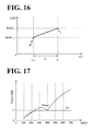
- FIG. 16 illustrates a definition of the peak value Ipeak_ n of the current IL through the inductance element 13 in each period T n .
- Ipeak_ n indicates the peak value of the current IL in the period T n
- Ipeak_ n ⁇ 1 indicates the peak value of the current IL in the period prior to the period T n .
- Time t n ⁇ 1 indicates the start time of the period T n
- Ipeak_ n and Ipeak_ n ⁇ 1 can be respectively represented using the following Formulae (29) and (30):
- I peak_ n ( VL _ n /L ) ⁇ T n (29)
- I peak_ n+1 I peak_ n +VL _ n ⁇ 1 /L ⁇ T n+1 (30)
- V(t) 0 in the periods T 0 and T 3 , as described above.
- the VB-side power P at the time of regeneration can represented using the following Formula (33).
- t 0 to t 2 are respectively denoted t 0 to t 2 .
- the VB-side power P in maximum modulation (hereinafter occasionally referred to as VB-side power P max ) can be represented using the following Formula (34). It is noted that the VB-side power P max is input power at the time of regeneration and output power at the time of charging.
- V(t) 0 in the periods T 0 and T 1 .
- the VB-side power P at the time of charging can represented using the following Formula (37).
- t 1 to t 3 are respectively denoted t 1 to t 3 .
- the VB-side power P max in maximum modulation can be represented using the following Formula (38):
- the reference power calculator 42 uses, for example, Formulae (34) and (38) to obtain the VB-side power P max in maximum modulation.
- the reference power calculator 42 is capable of obtaining the voltage VB and the voltage VPN from the voltage detectors 17 and 18 , and obtaining the carrier period Tc, the winding coil ratio N, and the minimal period T 1 min from an internal storage of the reference power calculator 42 or from the storage 50 .
- Formulae (33) and (37) can be represented using the following Formula (39):
- T 1 min T 3 min
- T 2 Tc/2 ⁇ 2 ⁇ T 1 min .
- T 1 min and T 3 min can be represented using the following Formula (40):
- the minimal periods T 1 min and T 3 min can be obtained using parameters such as the inductance value L of the inductance element 13 , the rated power P rate of the DC-to-DC converter 1 , the carrier period Tc, and the voltage VPN.
- the minimal periods T 1 min and T 3 min are 2.647 [usec], according to Formula (40).
- the reference period calculator 41 is capable of calculating the minimal periods T 1 min and T 3 min using, for example, Formula (40) and storing the obtained minimal periods T 1 min and T 3 min in the storage 50 or another storage.
- FIG. 17 illustrates an exemplary relationship between the VB-side power P max in maximum modulation calculated by the reference power calculator 42 and power P o , which the DC-to-DC converter 1 is able to output.
- the ratio calculator 43 calculates the ratio D ref based on the VB-side power P max in maximum modulation and the power command P ref .
- the ratio calculator 43 calculates the square root ratio, D p , of the VB-side power P max in maximum modulation and the power command P ref to each other (see Formula (41)), and sets the square root ratio D p as the ratio D ref .
- D p ⁇ ( P ref /P max ) (41)
- the control period calculator 44 calculates the period commands T 1 ref , T 2 ref , and T 3 ref based on the periods T 1 max , T 2 max , and T 3 max and based on the ratio D ref .
- the control period calculator 44 performs calculations represented by, for example, Formulae (42) to (44) to obtain the period commands T 1 ref , T 2 ref , and T 3 ref .
- T 1 ref T 1 max ⁇ D ref (42)
- T 2 ref T 2 max ⁇ D ref (43)
- T 3 ref T 3 max ⁇ D ref (44)
- FIG. 18 illustrates an example of the current IL at VB ⁇ N ⁇ VPN.
- FIG. 20 illustrates an example of the current IL at VB>N ⁇ VPN.
- current IL max indicates the current IL flowing through the inductance element 13 when the power command P ref is equivalent to the rated power P rate of the DC-to-DC converter 1 (in the example illustrated in FIG. 17 , 11 kW).
- periods T 1 lim , to T 3 lim respectively indicate the periods T 1 , T 2 , and T 3 that are in the case where the power command P ref is equivalent to the rated power P rate of the DC-to-DC converter 1 .
- the period adjustor 22 sets the ratio of the periods T 1 , T 2 , and T 3 to each other based on the ratio of the periods T 1 max , T 2 max , and T 3 max to each other, and adjusts the periods T 1 , T 2 , and T 3 based on the power command P ref .
- This configuration enables the period adjustor 22 to readily obtain the periods T 1 , T 2 , and T 3 , without complicated calculations, while minimizing the current flowing through the transformer 12 .
- the period adjustor 22 calculates the periods T 1 max , T 2 max , and T 3 max to elongate the second period T 2 . This configuration enables the period adjustor 22 to minimize the current flowing through the transformer 12 more effectively in cases of higher levels of input power or output power.
- the period adjustor 22 also calculates the periods T 1 max , T 2 max , and T 3 max based on the voltage VB and the voltage VPN. This configuration enables the period adjustor 22 to appropriately eliminate or minimize degradation of power conversion efficiency in the DC-to-DC converter 1 even when the voltage VB and the voltage VPN have changed.
- the period adjustor 22 also calculates the square root ratio D p of the VB-side power P max in maximum modulation and the power command P ref to each other, and multiplies the square root ratio D p by the periods T 1 max , T 2 max , and T 3 max to obtain the periods T 1 , T 2 , and T 3 .
- This configuration enables the period adjustor 22 to calculate with improved accuracy the operation periods of the first switching circuit 10 and the second switching circuit 11 based on the power command P ref .
- the switch driver 23 generates drive signals S 1 to S 8 based on the period commands T 1 ref , T 2 ref , and T 3 ref generated by the period adjustor 22 to on-off control the switching elements Q 1 to Q 8 of the first switching circuit 10 and the second switching circuit 11 .
- the switch driver 23 in controlling the first switching circuit 10 and the second switching circuit 11 , the switch driver 23 generates the drive signals S 1 to S 8 to make the periods T 1 , T 2 , and T 3 respectively coincide with the period commands T 1 ref , T 2 ref , and T 3 ref .
- FIG. 21 is a flowchart of DC-to-DC conversion processing performed by the DC-to-DC converter 1 .
- the DC-to-DC conversion processing illustrated in FIG. 21 is repeated by the DC-to-DC converter 1 .
- the controller 20 of the DC-to-DC converter 1 generates the power command P ref to, for example, maximize the supplied power PB from the power generator 4 (step S 10 ).
- the controller 20 Based on the voltage VB and the voltage VPN, the controller 20 generates the period commands T 1 ref , T 2 ref , and T 3 ref , and adjusts the periods of application of the voltage VB (which is a non-limiting example of one of the first voltage and second voltage recited in the appended claims) and the voltage VPN (which is a non-limiting example of the another one of the first voltage and second voltage recited in the appended claims) (step S 11 ).
- the period of application of the voltage VB is a period of time for which the voltage VB is applied from the first switching circuit 10 to the AC side.
- the period of application of the voltage VPN is a period of time for which the voltage VPN is applied from the second switching circuit 11 to the AC side.
- the controller 20 causes the first switching circuit 10 to operate for a period of time corresponding to the period commands T 1 ref and T 2 ref so as to cause the first switching circuit 10 to apply the voltage VB to the series circuit made up of the inductance element 13 and the primary winding coil of the transformer 12 (step S 12 ).
- the controller 20 also causes the second switching circuit 11 to operate for a period of time corresponding to the period commands T 2 ref and T 3 ref so as to cause the second switching circuit 11 to apply the voltage VPN to the secondary winding coil of the transformer 12 (step S 13 ).
- step S 14 the controller 20 determines whether to end the control processing illustrated in FIG. 21 . For example, when a stop command has been input from an operation section, not illustrated, the controller 20 determines to end the control processing illustrated in FIG. 21 . When the controller 20 has determined to end the control processing illustrated in FIG. 21 (Yes at step S 14 ), the controller 20 ends the control. When the controller 20 has determined not to end the control processing illustrated in FIG. 21 (No at step S 14 ), the controller 20 moves to step S 10 .
- Steps S 12 and S 13 are cases where the power conversion direction is the regeneration direction.
- the controller 20 causes the second switching circuit 11 to operate for a period of time corresponding to the period commands T 1 ref and T 2 ref so as to cause the voltage VPN to be applied to the secondary winding coil of the transformer 12 .
- the controller 20 causes the first switching circuit 10 to operate for a period of time corresponding to the period commands T 2 ref and T 3 ref so as to cause the voltage VB to be applied to the inductance element 13 and the primary winding coil of the transformer 12 , which are connected in series to each other.
- FIG. 22 is a flowchart of step S 11 illustrated in FIG. 21 .
- the controller 20 calculates the periods T 1 max , T 2 max , and T 3 max based on, for example, the voltage VB and the voltage VPN (step S 20 ).
- the controller 20 calculates the VB-side power P max in maximum modulation based on the periods T 1 max and T 2 max or based on the periods T 2 max and T 3 max (step S 21 ). Then, the controller 20 calculates the ratio D ref based on the VB-side power P max in maximum modulation and based on the power command P ref (step S 22 ). Next, the controller 20 multiplies the periods T 1 max , T 2 max , and T 3 max by the ratio D ref to calculate the period commands T 1 ref , T 2 ref , and T 3 ref (step S 23 ).
- the DC-to-DC converter 1 includes first means for applying a first voltage, second means for applying a second voltage, and third means for adjusting the periods of application of the first voltage and the second voltage.
- the first means applies a first voltage (which is a non-limiting example of the first voltage recited in the appended claims) to the primary winding coil (which is non-limiting example of the first winding coil recited in the appended claims) of the transformer 12 .
- the second means applies a second voltage (which is a non-limiting example of the second voltage recited in the appended claims) to the secondary winding coil (which is non-limiting example of the second winding coil recited in the appended claims) of the transformer 12 for a period between a point of time during application of the first voltage and a point of time after the application of the first voltage by the first means. At least one of the first voltage and the second voltage is applied through the inductance element 13 .
- the third means Based on a reference ratio that is set between a first application period of the first voltage applied by the first means and a second application period of the second voltage applied by the second means and that is based on reference input power or reference output power, the third means sets a non-reference ratio of the first application period of the first voltage and the second application period of the second voltage to each other.
- the non-reference ratio is based on non-reference power different from the reference input power or the reference output power.
- the period adjustor 22 illustrated in FIG. 3 uses input power as the reference power.
- the period adjustor 22 may use output power as the reference power.
- the minimal periods T 1 min and T 3 min can be obtained in a manner similar to Formula (40), using parameters such as the inductance value L, the rated power P rate , the carrier period Tc, the voltage VPN, and the voltage VB.
- the rated power P rate is the maximum rated power that the DC-to-DC converter 1 is able to output.
- the reference power calculator 42 performs calculations represented by Formulae (34) to (38) with the VPN-side power in maximum modulation set at P max (hereinafter occasionally referred to as VPN-side power P max ), and the ratio calculator 43 calculates the ratio D ref based on the VPN-side power P max in maximum modulation and the power command P ref .
- the power command P ref is an output power command that is generated by the command generator 21 at the time of regeneration to, for example, maximize the supplied power PB.
- the period adjustor 22 illustrated in FIG. 3 obtains the minimal periods T 1 min and T 3 min to maximize the second period T 2 .
- the period adjustor 22 may obtain the minimal periods T 1 min and T 3 min to maximize the second period T 2 when VB is not equivalent to N ⁇ VPN.
- the period adjustor 22 may obtain the minimal periods T 2 min and T 3 min to maximize the first period T 1 , and calculate the periods T 1 max , T 2 max , and T 3 max based on the minimal periods T 2 min and T 3 min .
- the period adjustor 22 uses the VB-side power P max in maximum modulation and the VPN-side power P max in maximum modulation as the reference power. In another possible embodiment, the period adjustor 22 may use power other than the VB-side power P max in maximum modulation or other than the VPN-side power P max in maximum modulation as the reference power.
- the reference power encompasses power that is based on voltage alone and power that is based on current alone.
- the controller 20 calculates the ratio D ref based on the VB-side power P max in maximum modulation and the power command P ref illustrated in FIG. 3 .
- the controller 20 may calculate the ratio D ref based on the output of the command generator 21 alone.
- the reference power calculator 42 and the ratio calculator 43 may not necessarily be provided.
- the command generator 21 obtains the ratio D ref (which is a non-limiting example of the power command recited in the appended claims) by controlling the voltage difference between the DC voltage command VB ref and the voltage VB to be zero.
- the DC-to-DC converter 1 performs DC-to-DC conversion using single-phase AC voltage.
- the DC-to-DC converter 1 may perform DC-to-DC conversion using three-phase AC voltage.
- the DC-to-DC converter 1 includes an inductance element for each phase and includes a first switching circuit and a second switching circuit for each inductance element.
- the first switching circuit and the second switching circuit each may be a half bridge circuit of a pair of switching elements connected in series to each other.
Applications Claiming Priority (1)
| Application Number | Priority Date | Filing Date | Title |
|---|---|---|---|
| PCT/JP2015/053277 WO2016125292A1 (fr) | 2015-02-05 | 2015-02-05 | Convertisseur continu-continu, convertisseur de courant électrique, système de production d'énergie électrique et procédé de conversion continu-continu |
Related Parent Applications (1)
| Application Number | Title | Priority Date | Filing Date |
|---|---|---|---|
| PCT/JP2015/053277 Continuation WO2016125292A1 (fr) | 2015-02-05 | 2015-02-05 | Convertisseur continu-continu, convertisseur de courant électrique, système de production d'énergie électrique et procédé de conversion continu-continu |
Publications (2)
| Publication Number | Publication Date |
|---|---|
| US20170310229A1 US20170310229A1 (en) | 2017-10-26 |
| US9985545B2 true US9985545B2 (en) | 2018-05-29 |
Family
ID=56563656
Family Applications (1)
| Application Number | Title | Priority Date | Filing Date |
|---|---|---|---|
| US15/649,792 Active US9985545B2 (en) | 2015-02-05 | 2017-07-14 | DC-to-DC converter, power converter, power generation system, and method for DC-to-DC conversion |
Country Status (3)
| Country | Link |
|---|---|
| US (1) | US9985545B2 (fr) |
| JP (1) | JP6150018B2 (fr) |
| WO (1) | WO2016125292A1 (fr) |
Cited By (1)
| Publication number | Priority date | Publication date | Assignee | Title |
|---|---|---|---|---|
| US10811985B2 (en) | 2016-08-26 | 2020-10-20 | General Electric Company | Power conversion system and an associated method thereof |
Families Citing this family (13)
| Publication number | Priority date | Publication date | Assignee | Title |
|---|---|---|---|---|
| CN110383663B (zh) | 2017-03-01 | 2020-04-24 | 株式会社村田制作所 | Dc-dc变换器 |
| JP6711449B2 (ja) * | 2017-03-14 | 2020-06-17 | 株式会社村田製作所 | Dc−dcコンバータ |
| JP6771156B2 (ja) * | 2017-03-29 | 2020-10-21 | パナソニックIpマネジメント株式会社 | 電力変換装置 |
| JP6575555B2 (ja) * | 2017-04-05 | 2019-09-18 | 株式会社豊田中央研究所 | 電力変換装置 |
| US10658936B2 (en) * | 2017-05-05 | 2020-05-19 | Macau University Of Science And Technology | System and method for controlling a converter circuit |
| US10050534B1 (en) * | 2017-05-15 | 2018-08-14 | Cummins Power Generation Ip, Inc. | Systems and methods for self-adaptive current control |
| US10110138B1 (en) | 2017-05-26 | 2018-10-23 | Cummins Power Generation Ip, Inc. | Soft-starting control method for electrical converter |
| JP6883489B2 (ja) * | 2017-08-22 | 2021-06-09 | ダイヤモンド電機株式会社 | コンバータ |
| CN109617414A (zh) * | 2018-12-07 | 2019-04-12 | 昂宝电子(上海)有限公司 | 使用霍尔效应传感器的开关模式功率转换器及其方法 |
| CN110768536B (zh) * | 2019-10-30 | 2020-08-14 | 北京机械设备研究所 | 一种双有源桥电路损耗控制方法 |
| WO2021124408A1 (fr) * | 2019-12-16 | 2021-06-24 | 三菱電機株式会社 | Convertisseur cc/cc et dispositif de conversion de puissance |
| JP7328916B2 (ja) | 2020-02-18 | 2023-08-17 | 三菱重工業株式会社 | 電源装置、制御装置、制御方法およびプログラム |
| CN113809928B (zh) * | 2021-09-16 | 2024-03-22 | 西安交通大学 | 一种基于功率前馈的dab变换器功率控制方法、介质及设备 |
Citations (11)
| Publication number | Priority date | Publication date | Assignee | Title |
|---|---|---|---|---|
| US7272021B2 (en) * | 1997-01-24 | 2007-09-18 | Synqor, Inc. | Power converter with isolated and regulated stages |
| JP2009044889A (ja) | 2007-08-09 | 2009-02-26 | Toyota Motor Corp | Dc−dcコンバータ装置 |
| JP2011130521A (ja) | 2009-12-15 | 2011-06-30 | Yokogawa Electric Corp | Dcdcコンバータ |
| US20110249472A1 (en) | 2010-04-01 | 2011-10-13 | Peregrine Power LLC | Pwm control of dual active bridge converters |
| JP2012065511A (ja) | 2010-09-17 | 2012-03-29 | Shindengen Electric Mfg Co Ltd | Dc/dcコンバータ |
| JP2013027201A (ja) | 2011-07-22 | 2013-02-04 | Ihi Corp | 直流電力変換装置 |
| WO2013173075A1 (fr) | 2012-05-18 | 2013-11-21 | General Electric Company | Convertisseur de puissance et procédé |
| JP2014239579A (ja) | 2013-06-06 | 2014-12-18 | 三菱電機株式会社 | Dc/dcコンバータおよびバッテリ充放電装置 |
| WO2015004825A1 (fr) | 2013-07-11 | 2015-01-15 | 三菱電機株式会社 | Convertisseur continu-continu |
| US9362832B2 (en) * | 2014-02-25 | 2016-06-07 | Telefonaktiebolaget L M Ericsson (Publ) | Intermediate bus architecture power supply |
| US9391531B2 (en) * | 2012-01-30 | 2016-07-12 | Telefonaktiebolaget L M Ericsson (Publ) | Controlling a switched mode power supply with maximised power efficiency |
-
2015
- 2015-02-05 WO PCT/JP2015/053277 patent/WO2016125292A1/fr active Application Filing
- 2015-02-05 JP JP2016549542A patent/JP6150018B2/ja active Active
-
2017
- 2017-07-14 US US15/649,792 patent/US9985545B2/en active Active
Patent Citations (13)
| Publication number | Priority date | Publication date | Assignee | Title |
|---|---|---|---|---|
| US7272021B2 (en) * | 1997-01-24 | 2007-09-18 | Synqor, Inc. | Power converter with isolated and regulated stages |
| JP2009044889A (ja) | 2007-08-09 | 2009-02-26 | Toyota Motor Corp | Dc−dcコンバータ装置 |
| JP2011130521A (ja) | 2009-12-15 | 2011-06-30 | Yokogawa Electric Corp | Dcdcコンバータ |
| US20110249472A1 (en) | 2010-04-01 | 2011-10-13 | Peregrine Power LLC | Pwm control of dual active bridge converters |
| JP2012065511A (ja) | 2010-09-17 | 2012-03-29 | Shindengen Electric Mfg Co Ltd | Dc/dcコンバータ |
| JP2013027201A (ja) | 2011-07-22 | 2013-02-04 | Ihi Corp | 直流電力変換装置 |
| US9391531B2 (en) * | 2012-01-30 | 2016-07-12 | Telefonaktiebolaget L M Ericsson (Publ) | Controlling a switched mode power supply with maximised power efficiency |
| WO2013173075A1 (fr) | 2012-05-18 | 2013-11-21 | General Electric Company | Convertisseur de puissance et procédé |
| US20130308344A1 (en) | 2012-05-18 | 2013-11-21 | Sebastian Pedro Rosado | Power converter and method |
| JP2014239579A (ja) | 2013-06-06 | 2014-12-18 | 三菱電機株式会社 | Dc/dcコンバータおよびバッテリ充放電装置 |
| WO2015004825A1 (fr) | 2013-07-11 | 2015-01-15 | 三菱電機株式会社 | Convertisseur continu-continu |
| US9641089B2 (en) | 2013-07-11 | 2017-05-02 | Mitsubishi Electric Corporation | DC-DC converter |
| US9362832B2 (en) * | 2014-02-25 | 2016-06-07 | Telefonaktiebolaget L M Ericsson (Publ) | Intermediate bus architecture power supply |
Non-Patent Citations (1)
| Title |
|---|
| International Search Report dated Apr. 21, 2015 in PCT/JP2015/053277 filed Feb. 5, 2015 (with English translation). |
Cited By (1)
| Publication number | Priority date | Publication date | Assignee | Title |
|---|---|---|---|---|
| US10811985B2 (en) | 2016-08-26 | 2020-10-20 | General Electric Company | Power conversion system and an associated method thereof |
Also Published As
| Publication number | Publication date |
|---|---|
| WO2016125292A1 (fr) | 2016-08-11 |
| JP6150018B2 (ja) | 2017-06-21 |
| US20170310229A1 (en) | 2017-10-26 |
| JPWO2016125292A1 (ja) | 2017-04-27 |
Similar Documents
| Publication | Publication Date | Title |
|---|---|---|
| US9985545B2 (en) | DC-to-DC converter, power converter, power generation system, and method for DC-to-DC conversion | |
| US11097368B2 (en) | Welding or cutting power supply using phase shift double forward converter circuit (PSDF) | |
| US10355526B2 (en) | Bi-directional inductive power transfer | |
| US11532990B2 (en) | Power conversion device that performs DC-to-DC conversion | |
| US9929663B1 (en) | Inductor protection during fast transient response in isolated voltage converters | |
| US9343986B2 (en) | Power converter with current feedback loop | |
| JP6153144B1 (ja) | Dc/dcコンバータの制御装置および制御方法 | |
| CN108377092B (zh) | 隔离式功率转换器及其控制方法 | |
| US11742766B2 (en) | Welding power supply with extended voltage characteristic | |
| US9160238B2 (en) | Power converter with current feedback loop | |
| US6917531B2 (en) | Power supply system | |
| US11050353B2 (en) | Power conversion device that generates switching signals | |
| CN112106288A (zh) | 电力变换装置以及电力变换系统 | |
| JP6366543B2 (ja) | Dc/dcコンバータ | |
| US11296608B2 (en) | Electric-power conversion apparatus | |
| US20140126251A1 (en) | Current-source power converting apparatus | |
| US9473040B2 (en) | Systems and methods for controlling active rectifiers | |
| WO2020129157A1 (fr) | Dispositif de conversion de puissance | |
| NZ582580A (en) | Controlling the relative phase of a pickup on a secondary side with respect to a converter on a primary side | |
| JP2000125575A (ja) | 正弦波入出力単相倍電圧交直変換回路の定サンプリング型pwm装置 | |
| WO2023122779A1 (fr) | Convertisseur auto-oscillant ayant une commande de fréquence variable et un décalage temporel au point minimum fixe pour une opération de commutation douce efficace | |
| CN116316646A (zh) | 有载调压装置、有载调压变压器及其控制方法 | |
| KR20150127855A (ko) | 동기형 저전압 직류직류 컨버터 | |
| JPH01136597A (ja) | 同期電動機の駆動装置 |
Legal Events
| Date | Code | Title | Description |
|---|---|---|---|
| AS | Assignment |
Owner name: KABUSHIKI KAISHA YASKAWA DENKI, JAPAN Free format text: ASSIGNMENT OF ASSIGNORS INTEREST;ASSIGNORS:FUJISAKI, SEIJI;ISHII, SADAO;IDE, KOZO;REEL/FRAME:043007/0549 Effective date: 20170711 |
|
| STCF | Information on status: patent grant |
Free format text: PATENTED CASE |
|
| MAFP | Maintenance fee payment |
Free format text: PAYMENT OF MAINTENANCE FEE, 4TH YEAR, LARGE ENTITY (ORIGINAL EVENT CODE: M1551); ENTITY STATUS OF PATENT OWNER: LARGE ENTITY Year of fee payment: 4 |