US9961287B2 - Image sensor - Google Patents
Image sensor Download PDFInfo
- Publication number
- US9961287B2 US9961287B2 US15/293,122 US201615293122A US9961287B2 US 9961287 B2 US9961287 B2 US 9961287B2 US 201615293122 A US201615293122 A US 201615293122A US 9961287 B2 US9961287 B2 US 9961287B2
- Authority
- US
- United States
- Prior art keywords
- analog
- digital conversion
- conversion units
- image sensor
- groups
- Prior art date
- Legal status (The legal status is an assumption and is not a legal conclusion. Google has not performed a legal analysis and makes no representation as to the accuracy of the status listed.)
- Active
Links
- 238000006243 chemical reaction Methods 0.000 claims abstract description 154
- 238000005070 sampling Methods 0.000 claims abstract description 109
- 239000011159 matrix material Substances 0.000 claims abstract description 17
- 230000000875 corresponding effect Effects 0.000 claims description 30
- 238000009792 diffusion process Methods 0.000 claims description 24
- 230000004044 response Effects 0.000 claims description 22
- 230000015654 memory Effects 0.000 claims description 18
- 230000002596 correlated effect Effects 0.000 claims description 14
- 238000000034 method Methods 0.000 description 45
- 230000008569 process Effects 0.000 description 45
- 238000010586 diagram Methods 0.000 description 35
- 230000005540 biological transmission Effects 0.000 description 9
- 230000008901 benefit Effects 0.000 description 4
- 239000003990 capacitor Substances 0.000 description 4
- 230000000295 complement effect Effects 0.000 description 2
- 230000000694 effects Effects 0.000 description 2
- 239000000470 constituent Substances 0.000 description 1
- 230000001276 controlling effect Effects 0.000 description 1
- 229910044991 metal oxide Inorganic materials 0.000 description 1
- 150000004706 metal oxides Chemical class 0.000 description 1
- 238000012986 modification Methods 0.000 description 1
- 230000004048 modification Effects 0.000 description 1
- 239000004065 semiconductor Substances 0.000 description 1
- 239000000758 substrate Substances 0.000 description 1
- 230000009466 transformation Effects 0.000 description 1
Images


Classifications
-
- H04N5/3742—
-
- H—ELECTRICITY
- H04—ELECTRIC COMMUNICATION TECHNIQUE
- H04N—PICTORIAL COMMUNICATION, e.g. TELEVISION
- H04N25/00—Circuitry of solid-state image sensors [SSIS]; Control thereof
- H04N25/70—SSIS architectures; Circuits associated therewith
- H04N25/76—Addressed sensors, e.g. MOS or CMOS sensors
- H04N25/767—Horizontal readout lines, multiplexers or registers
-
- H—ELECTRICITY
- H01—ELECTRIC ELEMENTS
- H01L—SEMICONDUCTOR DEVICES NOT COVERED BY CLASS H10
- H01L27/00—Devices consisting of a plurality of semiconductor or other solid-state components formed in or on a common substrate
- H01L27/14—Devices consisting of a plurality of semiconductor or other solid-state components formed in or on a common substrate including semiconductor components sensitive to infrared radiation, light, electromagnetic radiation of shorter wavelength or corpuscular radiation and specially adapted either for the conversion of the energy of such radiation into electrical energy or for the control of electrical energy by such radiation
- H01L27/144—Devices controlled by radiation
- H01L27/146—Imager structures
- H01L27/14601—Structural or functional details thereof
- H01L27/14609—Pixel-elements with integrated switching, control, storage or amplification elements
- H01L27/14612—Pixel-elements with integrated switching, control, storage or amplification elements involving a transistor
-
- H—ELECTRICITY
- H01—ELECTRIC ELEMENTS
- H01L—SEMICONDUCTOR DEVICES NOT COVERED BY CLASS H10
- H01L27/00—Devices consisting of a plurality of semiconductor or other solid-state components formed in or on a common substrate
- H01L27/14—Devices consisting of a plurality of semiconductor or other solid-state components formed in or on a common substrate including semiconductor components sensitive to infrared radiation, light, electromagnetic radiation of shorter wavelength or corpuscular radiation and specially adapted either for the conversion of the energy of such radiation into electrical energy or for the control of electrical energy by such radiation
- H01L27/144—Devices controlled by radiation
- H01L27/146—Imager structures
- H01L27/14643—Photodiode arrays; MOS imagers
-
- H—ELECTRICITY
- H04—ELECTRIC COMMUNICATION TECHNIQUE
- H04N—PICTORIAL COMMUNICATION, e.g. TELEVISION
- H04N25/00—Circuitry of solid-state image sensors [SSIS]; Control thereof
- H04N25/40—Extracting pixel data from image sensors by controlling scanning circuits, e.g. by modifying the number of pixels sampled or to be sampled
- H04N25/46—Extracting pixel data from image sensors by controlling scanning circuits, e.g. by modifying the number of pixels sampled or to be sampled by combining or binning pixels
-
- H—ELECTRICITY
- H04—ELECTRIC COMMUNICATION TECHNIQUE
- H04N—PICTORIAL COMMUNICATION, e.g. TELEVISION
- H04N25/00—Circuitry of solid-state image sensors [SSIS]; Control thereof
- H04N25/70—SSIS architectures; Circuits associated therewith
- H04N25/709—Circuitry for control of the power supply
-
- H—ELECTRICITY
- H04—ELECTRIC COMMUNICATION TECHNIQUE
- H04N—PICTORIAL COMMUNICATION, e.g. TELEVISION
- H04N25/00—Circuitry of solid-state image sensors [SSIS]; Control thereof
- H04N25/70—SSIS architectures; Circuits associated therewith
- H04N25/71—Charge-coupled device [CCD] sensors; Charge-transfer registers specially adapted for CCD sensors
- H04N25/75—Circuitry for providing, modifying or processing image signals from the pixel array
-
- H—ELECTRICITY
- H04—ELECTRIC COMMUNICATION TECHNIQUE
- H04N—PICTORIAL COMMUNICATION, e.g. TELEVISION
- H04N25/00—Circuitry of solid-state image sensors [SSIS]; Control thereof
- H04N25/70—SSIS architectures; Circuits associated therewith
- H04N25/76—Addressed sensors, e.g. MOS or CMOS sensors
- H04N25/77—Pixel circuitry, e.g. memories, A/D converters, pixel amplifiers, shared circuits or shared components
- H04N25/772—Pixel circuitry, e.g. memories, A/D converters, pixel amplifiers, shared circuits or shared components comprising A/D, V/T, V/F, I/T or I/F converters
-
- H04N5/347—
-
- H04N5/3698—
-
- H04N5/37455—
-
- H04N5/378—
Definitions
- Embodiments of the present invention relate to an image sensor.
- one frame may include an array of N ⁇ M unit pixels.
- CMOS complementary metal-oxide semiconductor
- the image sensor may use a low resolution mode if the data processing speed needs to increase (e.g., a moving image mode). In the low resolution mode, all unit pixels do not output signals, but some unit pixels may output signals.
- the low resolution mode of the image sensor may be implemented using a subsampling mode and a binning mode.
- embodiments of the present invention are directed to an image sensor capable of reducing power consumption of an analog-digital conversion block and increasing a frame rate.
- an image sensor may include a pixel array including a plurality of unit pixels in a matrix including rows and columns, the matrix being divided into a plurality of groups, each of the plurality of groups including two or more different columns, a binning sampling unit configured to sample outputs of unit pixels in each of the plurality of groups and output binning sampling signals (e.g., based on or according to the sampled outputs), and an analog-digital conversion block including a plurality of analog-digital conversion units corresponding to the columns, the analog-digital conversion units having first and second analog-digital conversion units, the analog-digital conversion units being configured to convert the binning sampling signals.
- the first analog-digital conversion units convert the binning sampling signals
- the second analog-digital conversion units are turned off.
- Each of the plurality of groups may include two or more adjacent columns.
- the plurality of groups may include first and second groups, and each of the first groups may include two or more adjacent odd-numbered columns, and each of the second groups may include two or more adjacent even-numbered columns.
- the pixel array may include sensing lines connected to the binning sampling unit and each of the sensing lines is connected to a corresponding unit pixel in a corresponding one of the columns.
- the binning sampling unit may include first switches configured to connect sensing lines corresponding to columns in each of the plurality of groups, and second switches between the sensing lines and the analog-digital conversion units.
- the binning sampling unit may further include third switches between a ground voltage or a ground potential and nodes between the sensing lines and the analog-digital conversion units.
- the image sensor may further include a selector configured to turn the first analog-digital conversion unit on and turn the second analog-digital conversion unit off.
- the image sensor may further include a memory including a plurality of latches configured to store outputs of the analog-digital conversion units.
- the image sensor may further include a column scanner configured to select first ones of the latches corresponding to the first analog-digital conversion units and read digital data in the selected first latches.
- Each of the plurality of analog-digital conversion units may include a correlated double sampling unit configured to perform correlated double sampling, and an analog-digital converter configured to convert an output of the correlated double sampling unit, where the correlated double sampling unit and the analog-digital converter of each of the second analog-digital conversion units may be turned off.
- an image sensor includes a pixel array including a plurality of unit pixels in a matrix including rows and columns, the matrix being divided into a plurality of groups, and each of the plurality of groups including two or more different columns, a binning sampling unit configured to sample outputs of unit pixels that belong to each of the plurality of groups and output binning sampling signals, an analog-digital conversion block including a plurality of analog-digital conversion units that correspond to the columns, the analog-digital conversion units comprising first analog-digital conversion units configured to convert the binning sampling signals, latches configured to store outputs of the plurality of analog-digital conversion units, and a column scanner configured to select first ones of the latches to store outputs of the first analog-digital conversion units and read digital data in the selected first latches.
- Each of the plurality of groups may include two or more adjacent columns.
- the plurality of groups may include first and second groups. Each of the first groups may include two or more adjacent odd-numbered columns and each of the second groups may include two or more adjacent even-numbered columns.
- the column scanner may generate scan signals configured to select the first latches and sequentially read the data in the first latches in response to the scan signals.
- Each of the unit pixels may include a photodiode, a floating diffusion area, a transfer transistor, a reset transistor, a drive transistor and a select transistor.
- an image sensor includes a pixel array including a plurality of unit pixels in a matrix including rows and columns, sensing lines, and readout circuits between the plurality of unit pixels and the sensing lines, the matrix being divided into a plurality of groups, and each of the plurality of groups including two or more different columns, a binning sampling unit configured to sample outputs of unit pixels in each of the plurality of groups and output binning sampling signals, and an analog-digital conversion block including a plurality of analog-digital conversion units corresponding to the columns, the analog-digital conversion units comprising first analog-digital conversion units configured to convert the binning sampling signals.
- Each of the unit pixels includes a photodiode, a floating diffusion area and a transfer transistor between the photodiode and the floating diffusion area.
- the unit pixels in each column are grouped into a plurality of subgroups, and the floating diffusion areas of the unit pixels in each of the plurality of subgroups are connected to and shared between each other.
- the readout circuit connects the shared floating diffusion areas and a corresponding one of the sensing lines.
- the second analog-digital conversion units may be turned off.
- the image sensor may further include latches configured to store outputs of the plurality of analog-digital conversion units and a column scanner configured to select first ones of the latches to store the outputs of the first analog-digital conversion units and read digital data in the selected first latches.
- Each of the plurality of subgroups may include two or more adjacent unit pixels included in each column.
- the plurality of subgroups may include first and second subgroups.
- Each of the first sub groups may include unit pixels of two or more adjacent odd-numbered rows of each column
- each of the second sub groups may include unit pixels of two or more adjacent even-numbered rows of each column.
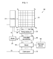
- FIG. 1 is diagram showing a configuration of an exemplary image sensor according to embodiments of the invention
- FIG. 2 is a diagram showing one or more embodiments of a pixel array unit, an analog-digital conversion block and a memory as shown in FIG. 1 ;
- FIG. 3 is a diagram showing one or more operations according to one or more embodiments of the image sensor shown in FIG. 1 ;
- FIG. 4 is a diagram showing one or more operations according to other embodiments of the image sensor shown in FIG. 1 ;
- FIG. 5 is a diagram showing an operation according to another embodiment of the image sensor shown in FIG. 1 ;
- FIG. 6 is a diagram showing an operation according to yet another embodiment of the image sensor shown in FIG. 1 ;
- FIG. 7 is a timing diagram of scan signals generated by an exemplary column scanner as shown in FIG. 3 ;
- FIG. 8 is a timing diagram of scan signals generated by an exemplary column as scanner shown in FIG. 4 ;
- FIG. 9A is a diagram showing ON and/or OFF states of first to third switches and ON and/or OFF states of analog-digital conversion units according to a first exemplary process or operation of the binning sampling unit of FIG. 3 ;
- FIG. 9B is a diagram showing ON and/or OFF states of first to third switches and ON and/or OFF states of analog-digital conversion units according to a second exemplary process or operation of the binning sampling unit of FIG. 3 ;
- FIG. 10A is a diagram showing ON and/or OFF states of first to third switches and ON and/or OFF states of analog-digital conversion units according to a first exemplary process or operation of the binning sampling unit of FIG. 4 ;
- FIG. 10B is a diagram showing ON and/or OFF states of first to third switches and ON and/or OFF states of analog-digital conversion units according to a second exemplary process or operation of the binning sampling unit of FIG. 4 ;
- FIG. 11 is a diagram showing an exemplary embodiment of a unit pixel in the pixel array shown in FIG. 1 ;
- FIG. 12 is a diagram showing another embodiment of the pixel array shown in FIG. 1 ;
- FIG. 13A is a timing diagram showing an exemplary process or operation of the pixel array of FIG. 12 in a first driving mode
- FIG. 13B is a timing diagram showing an exemplary process or operation of the pixel array of FIG. 12 in a second driving mode
- FIG. 14 is a diagram showing another embodiment of the pixel array shown in FIG. 1 ;
- FIG. 15A is a timing diagram showing an exemplary process or operation of the pixel array diagram of FIG. 14 in a first driving mode
- FIG. 15B is a timing chart showing an exemplary process or operation of the pixel array of FIG. 14 in a second driving mode.
- FIG. 1 is diagram showing a configuration of an exemplary image sensor 100 according to one or more embodiments
- FIG. 2 is a diagram showing one or more embodiments of the pixel array 120 , the analog-digital conversion block 149 and the memory 160 shown in FIG. 1 .
- the exemplary image sensor 100 includes a controller 110 , a pixel array unit 120 , a binning sampling unit 130 , an analog-digital conversion block 140 , a selector 150 , a memory 160 and a column scanner 170 .
- the image sensor 100 may further include a digital signal processor 180 .
- the controller 110 outputs a first control signal (e.g., a reset signal RX, a transmission signal TX, a selection signal SX) configured to control the pixel array 120 , a second control signal (e.g., BS) configured to control the binning sampling unit 130 , a third control signal (e.g., SC) configured to control the selector 150 , and a fourth signal (e.g., CS) configured to control the column scanner 170 .
- a first control signal e.g., a reset signal RX, a transmission signal TX, a selection signal SX
- BS second control signal
- SC control signal
- CS fourth signal
- the controller 110 may include a timing controller configured to generate a timing signal and/or a control signal.
- the controller 110 may include a row driver configured to generate a first control signal for driving a plurality of unit pixels (e.g., in a row of the pixel array) based on the timing signal provided by the timing controller.
- the pixel array 120 may include a plurality of unit pixels P 11 to Pnm (n and m being natural numbers greater than 1), and the plurality of unit pixels P 11 to Pnm may be arranged in a matrix including rows and columns.
- Each of the unit pixels P 11 to Pnm may comprise a photoelectric transformation element configured to sense light and transform the sensed light into an electric signal.
- the pixel array 120 may include sensing lines L 1 to Lm (m being a natural number greater than 1) connected to the unit pixels P 11 to Pnm.
- the pixel array 120 outputs sensing signals al to am (m being a natural number greater than 1) on the sensing lines L 1 to Lm.
- each of the sensing lines L 1 to Lm may be connected to each of the output terminals of the unit pixels P 11 to Pnm in a corresponding one of the columns.
- the binning sampling unit 130 receives outputs of two or more unit pixels from among the unit pixels P 11 to Pnm connected to the sensing lines L 1 to Lm and outputs binning sampling signals b 1 to bk (e.g., 1 ⁇ k ⁇ m) based on a second control signal BS.
- the binning sampling signals b 1 to bk may be a sum or average of the outputs of the selected two or more unit pixels, without being limited thereto.
- the binning sampling unit 130 may sample outputs of the unit pixels belonging to two or more different columns and output binning sampling signals b 1 to bk (e.g., 1 ⁇ k ⁇ m) according to the sampled outputs.
- the unit pixels belonging to two or more different columns may have identical exposure times.
- the exposure time may be a period from reset operation of a photodiode in a unit pixel to the transmission of charges generated by the light received by the photodiode to a floating diffusion area of the unit pixel.
- the binning sampling unit 130 may sample outputs of two or more sensing lines from among the sensing lines L 1 to Lm and output the binning sampling signals b 1 to bk according to the sampled outputs.
- the pixel array may be divided into a plurality of groups, and each of the plurality of groups may include two or more different columns. The columns in each group may not overlap each other.
- the groups may include two or more adjacent columns.
- the groups may include first and second groups.
- the first group may include two or more adjacent odd-numbered columns, and the second group may include two or more adjacent even-numbered columns.
- the analog-digital conversion block 140 converts the analog binning sampling signals b 1 to bk to digital signals.
- the binning sampling signals b 1 to bk are analog signals output from the binning sampling unit 130 , and the analog-digital conversion block 140 outputs digital signals C 1 to Ci (i being a natural number greater than 1) according to the conversion, based on a selection signal ST.
- the analog-digital conversion block 140 may include a plurality of analog-digital conversion units 140 - 1 to 140 - m ( FIG. 2 ).
- the plurality of analog-digital conversion units 140 - 1 to 140 - m may include (i) correlated double sampling units 210 - 1 to 210 - m configured to perform correlated double sampling in order to reduce or cancel any fixed pattern noise (e.g., unique fixed pattern noise from the pixels) and (ii) analog-digital converters 220 - 1 to 220 - m convert the analog outputs of the correlated double sampling units 210 - 1 to 210 - m to digital signals (e.g., C 1 to Ci).
- any fixed pattern noise e.g., unique fixed pattern noise from the pixels
- analog-digital converters 220 - 1 to 220 - m convert the analog outputs of the correlated double sampling units 210 - 1 to 210 - m to digital signals (e.g., C 1 to Ci).
- the plurality of analog-digital conversion units 140 - 1 to 140 - m may correspond to the sensing lines L 1 to Lm (e.g., in a 1:1 relationship).
- each of the plurality of analog-digital conversion units 140 - 1 to 140 - m may correspond to one of the sensing lines L 1 to Lm.
- the binning sampling signals b 1 to bk may be selectively provided to k analog-digital conversion units from among the m analog-digital conversion units 140 - 1 to 140 - m.
- the selector 150 may output selection signals ST 11 to ST 1 m configured to control the plurality of analog-digital conversion units 140 - 1 to 140 - m based on the third control signal SC.
- the plurality of analog-digital conversion units 140 - 1 to 140 - m may selectively operate in response to the selection signals ST 11 to ST 1 m .
- a group or set of first analog-digital conversion units e.g., analog-digital conversion units 140 - 1 , 140 - 3 . . . 140 - m ⁇ 1, where m is an even integer of 6 or more
- a group or set of second analog-digital conversion unit e.g., analog-digital conversion units 140 - 2 , 140 - 4 . . . 140 - m
- second analog-digital conversion unit e.g., analog-digital conversion units 140 - 2 , 140 - 4 . . . 140 - m
- the second analog-digital conversion units may be turned off.
- an operating voltage may be supplied to the first analog-digital conversion units to turn the first analog-digital conversion units on, and the operating voltage or its complement may be supplied to the second analog-digital conversion units to turn the second analog-digital conversion units off.
- the binning sampling signals b 1 to bk are supplied to the first analog-digital conversion units and the binning sampling signals b 1 to bk (e.g., the active binning sampling signals) are not supplied to the second analog-digital conversion units.
- the first analog-digital conversion units may output the digital signals C 1 to Ci by performing an analog-digital conversion on the binning sampling signals.
- the embodiments can reduce power consumption of the analog-digital conversion block.
- the memory 160 may store outputs of the analog-digital conversion units 140 - 1 to 140 - m and read and/or output the digital signals C 1 to Ci to the digital signal processor 180 in response to the control signals CS 1 to CSm of the column scanner 170 .
- the memory 160 may include a plurality of latches 160 - 1 to 160 - m or a plurality of capacitors (e.g., one transistor-one capacitor memory cells such as those commonly found in dynamic random access memories [DRAMs]).
- the plurality of latches 160 - 1 to 160 - m or the plurality of capacitors correspond to the plurality of analog-digital conversion units 140 - 1 to 140 - m.
- each of the plurality of latches 160 - 1 to 160 - m may store a corresponding one of the outputs of the plurality of analog-digital conversion units 140 - 1 to 140 - m.
- first ones of the plurality of latches 160 - 1 to 160 - m may correspond to the first analog-digital conversion units
- second ones of the plurality of latches 160 - 1 to 160 - m may correspond to the second analog-digital conversion units.
- the column scanner 170 may output control signals CS 1 to CSm configured to control the memory 160 based on the fourth control signal CS received from the controller 110 .
- the column scanner 170 may generate the control signals CS 1 to CSm to select and read the first latches storing the digital signals C 1 to Ci.
- the first latches storing the digital signals C 1 to Ci may be selected from among the plurality of latches 160 - 1 to 160 - m of the memory 160 by the first control signals CS 1 to CSm. Data stored in the first latch may be sequentially read in response to a clock signal CLK (see, e.g., FIG. 7 ) from the controller 110 and may be transmitted to the digital signal processor 180 .
- CLK clock signal
- embodiments of the invention may improve the speed for reading the data stored in the memory 160 and thus can shorten the time to scan one row of the pixel array 120 .
- the column scanner 170 may select all of the latches 160 - 1 to 160 - m and read the data stored in the latches 160 - 1 to 160 - m.
- the digital signal processor 180 processes the digital signals C 1 to Ci received from the memory 160 .
- FIG. 3 is a diagram showing a process or operation according to one or more embodiments of the image sensor shown in FIG. 1 .
- FIG. 2 The same reference numerals as FIG. 2 indicate the same components in FIG. 3 , which will be described briefly or omitted.
- FIG. 3 may show a monochrome type image sensor for sensing a grayscale image.
- the binning sampling unit 130 a may sample outputs of the unit pixels belonging to two adjacent columns and output binning sampling signals b 1 to bk (e.g., 1 ⁇ k ⁇ m) according to the sampled outputs and/or based on a second control signal BS.
- binning sampling signals b 1 to bk e.g., 1 ⁇ k ⁇ m
- the binning sampling unit 130 a may include a plurality of switches and a plurality of capacitors.
- the second control signal BS may be a signal for controlling the plurality of switches.
- the binning sampling unit 130 a may further include at least one resistor.
- the binning sampling signals b 1 to bk may be provided to first analog-digital conversion unit 140 - 1 to 140 -( m ⁇ 1) among the plurality of analog-digital conversion units 140 - 1 to 140 - m .
- the first analog-digital conversion units may include one or more odd-numbered analog-digital conversion units corresponding to the odd-numbered sensing lines, without being limited thereto.
- a voltage or active signal is supplied to the first (e.g., odd-numbered) analog-digital conversion units 140 - 1 to 140 -( m ⁇ 1) to turn on the first analog-digital conversion units 140 - 1 to 140 -( m ⁇ 1), whereas the voltage or active signal is not supplied to the remaining (e.g., even-numbered) analog-digital conversion units 140 - 2 to 140 - m to turn off the remaining analog-digital conversion units 140 - 2 to 140 - m.
- a bias current is supplied to first analog-digital conversion units 140 - 1 to 140 -( m ⁇ 1) to turn on the first analog-digital conversion units 140 - 1 to 140 -( m ⁇ 1), whereas the bias current is not supplied to the remaining analog-digital conversion units 140 - 2 to 140 - m to turn off the remaining analog-digital conversion units 140 - 2 to 140 - m.
- the first correlated double sampling units 210 - 1 to 210 -( m ⁇ 1) and the first analog-digital conversion units 220 - 1 to 220 -( m ⁇ 1) of the first analog-digital conversion units 140 - 1 to 140 -( m ⁇ 1) may all be turned on.
- the second correlated double sampling units 210 - 2 to 210 - m and the second analog-digital conversion units 220 - 2 to 220 - m of the second analog-digital conversion units 140 - 2 to 140 - m may all be turned off. Therefore, according to one or more embodiments, it is possible to reduce power consumption.
- the outputs of the first analog-digital conversion units 140 - 1 to 140 -( m ⁇ 1) may be stored in first latches 160 - 1 to 160 -( m ⁇ 1) corresponding to the first analog-digital conversion units 140 - 1 to 140 -( m ⁇ 1) among the latches 160 - 1 to 160 - m of the memory 160 .
- the column scanner 170 may generate scan signals CS 1 to CS-( m ⁇ 1) for selecting first latches to be read from among the latches 160 - 1 to 160 - m of the memory 160 .
- data stored in the first latches 160 - 1 to 160 -( m ⁇ 1) may be sequentially read.
- FIG. 7 is a timing chart of scan signals CS 1 to CS-( m ⁇ 1) generated by an exemplary column scanner 170 as shown in FIG. 3 .
- the column scanner 170 may generate scan signals CS 1 to CSm ⁇ 1 for reading first latches 160 - 1 to 160 -( m ⁇ 1) (e.g., odd-numbered latches) in response to a clock signal CLK.
- first latches 160 - 1 to 160 -( m ⁇ 1) e.g., odd-numbered latches
- CLK clock signal
- data D 1 to Dm ⁇ 1 stored in the first latches are sequentially transmitted to the digital signal processor 180 .
- a scan of one row of the pixel array 120 may be completed.
- FIG. 4 is a diagram showing a process or operation according to one or more other embodiments of the image sensor shown in FIG. 1 .
- the embodiment(s) of FIG. 4 may relate to a Bayer-type image sensor for sensing a color (e.g., RGB) image.
- a color e.g., RGB
- the binning sampling unit 130 b may sample outputs of unit pixels belonging to two adjacent odd-numbered columns of the pixel array 120 , and output first binning sampling signals b 11 to b 1 ( k ⁇ 1) according to the sampled outputs based on a second control signal BS.
- the binning sampling unit 130 b may sample outputs of unit pixels belonging to two adjacent even-numbered columns of the pixel array 120 , and output first binning sampling signals b 12 to b 1 k (e.g., 1 ⁇ k ⁇ m) according to the sampled based on the second control signal BS.
- the binning sampling signals b 11 to b 1 k may be supplied to the first analog-digital conversion units 140 - 1 , 140 - 2 , 140 - 5 , 140 - 6 . . . 140 - m ), without being limited thereto.
- a voltage or signal is supplied to the first analog-digital conversion units 140 - 1 , 140 - 2 , 140 - 5 , 140 - 6 , etc., to turn on the first analog-digital conversion units 140 - 1 , 140 - 2 , 140 - 5 , 140 - 6 , etc.
- the voltage or signal is not supplied to the remaining analog-digital conversion units to turn off the remaining analog-digital conversion units 140 - 2 to 140 - m . Therefore, according to embodiments of the invention, it may be possible to reduce power consumption in the analog-digital conversion block 140 .
- the outputs of the first analog-digital conversion units 140 - 1 , 140 - 2 , 140 - 5 , 140 - 6 , etc., may be stored in first latches 160 - 1 , 160 - 2 , 160 - 5 , 160 - 6 . . . 160 - m corresponding to the first analog-digital conversion units 140 - 1 , 140 - 2 , 140 - 5 , 140 - 6 , 140 - m.
- FIG. 8 is a timing chart of scan signals generated by the exemplary column scanner 170 shown in FIG. 4 .
- the column scanner 170 may generate scan signals CS 1 , CS 2 , CS 5 , CS 6 . . . and CSq for reading first latches 160 - 1 , 160 - 2 , 160 - 5 , 160 - 6 . . . in response to a clock signal CLK.
- the binning sampling unit 130 shown in FIG. 2 may output the signals of the unit pixels belonging to each column of the pixel array 120 to the analog-digital conversion units corresponding to each column. In this case, it may be possible to perform a normal mode process or operation without performing a horizontal binning process or operation by the binning sampling unit 130 .
- FIG. 5 is a diagram showing a process or an operation according to one or more further embodiments of the image sensor shown in FIG. 1 .
- the binning sampling unit 130 c samples the outputs of the unit pixels belonging to each column of the pixel array 120 and outputs sampling signals SP 1 to SPm according to the sampled outputs, based on a second control signal BS.
- FIG. 5 shows a normal process or operation, rather than a binning process or operation.
- Each of the plurality of analog-digital conversion units 140 - 1 to 140 - m converts a corresponding analog sampling signals SP 1 to SPm to a digital signal.
- Each of the plurality of latches 160 stores a corresponding one of the outputs of the plurality of analog-digital conversion units 140 - 1 to 140 - m.
- the column scanner 170 reads the data stored in the plurality of latches 160 and transmits the data to the digital signal processor 180 .
- FIG. 6 is a diagram showing a process or an operation according to one or more further embodiments of the image sensor shown in FIG. 1 .
- the binning sampling unit 130 d samples the outputs of the unit pixels belonging to odd-numbered or even-numbered columns of the pixel array 120 and outputs sampling signals SP 1 to SPk according to the sampled outputs, based on a second signal BS.
- FIG. 5 shows a skipping operation.
- the odd-numbered or even-numbered analog-digital conversion units may convert corresponding analog sampling signals SP 1 to SPk and output the converted digital signal.
- the odd-numbered or even-numbered latches store the outputs of the odd-numbered or even-numbered analog-digital conversion units.
- the column scanner 170 reads the data stored in the odd-numbered or even-numbered latches and transmits the data to the digital signal processor 180 .
- the binning sampling unit 130 may include first switches for connecting the sensing lines corresponding to the columns included in the plurality of groups. In addition, the binning sampling unit 130 may include second switches between the sensing lines and the analog-digital conversion units.
- the binning sampling unit 130 may further include third switches between a ground voltage or ground potential and nodes connecting the sensing lines and the analog-digital conversion units.
- FIG. 9A is a diagram showing one or more embodiments of the binning sampling unit 130 a of FIG. 3 .
- the binning sampling unit 130 a may include first switches 131 a - 1 to 131 a - j (j being a natural number greater than 1) between two adjacent sensing lines L 1 and L 2 , L 3 and L 4 . . . Lm ⁇ 1 and Lm, and second switches 132 - 1 to 132 - m between the sensing lines L 1 to Lm and the analog digital conversion units 140 - 1 to 140 - m .
- the binning sampling unit 130 a may include third switches 134 - 1 to 134 - m between the ground voltage or ground potential GND and connection nodes N 1 to Nm, which are between the sensing lines L 1 to Lm and the analog-digital conversion units 140 - 1 to 140 - m .
- the binning sampling unit 130 a may further include a constant current source 133 between the sensing lines L 1 to Lm and the ground voltage or ground potential GND.
- each of the first switches 131 a - 1 to 131 a - j may be between the two different and/or adjacent sensing lines (e.g., L 1 and L 2 , L 3 and L 4 . . . Lm ⁇ 1 and Lm) among the sensing lines L 1 to Lm.
- the two different and/or adjacent sensing lines e.g., L 1 and L 2 , L 3 and L 4 . . . Lm ⁇ 1 and Lm
- each of the second switches 132 - 1 to 132 - m may be between a corresponding one of the sensing lines L 1 to Lm and a corresponding one of the analog-digital conversion units 140 - 1 to 140 - m (e.g., between sensing line L 1 and analog-digital conversion unit 140 - 1 , sensing line L 2 and analog-digital conversion unit 140 - 2 , etc.).
- each of the third switches 134 - 1 to 134 - m may be between one of the connection nodes N 1 to Nm and the ground voltage or ground potential GND.
- the constant current source 133 may be between the sensing lines L 1 to Lm and the ground voltage or ground potential GND.
- FIG. 9A shows the ON and OFF states of the first to third switches and the ON and OFF states of the analog-digital conversion units 140 - 1 to 140 - m according to a first process or operation of the binning sampling unit 130 a of FIG. 3 .
- the first process or operation of the binning sampling unit 130 a may be a horizontal binning process or operation.
- the third switches 134 - 1 to 134 -( m ⁇ 1) connected to the turned-on analog-digital conversion units 140 - 1 to 140 -( m ⁇ 1) are turned off.
- the third switches 134 - 2 to 134 - m connected to the turned-off analog-digital conversion units 140 - 2 to 140 - m are turned on to prevent current leakage.
- FIG. 9B is a diagram showing the ON and/or OFF states of the first to third switches and the ON and/or OFF states of the analog-digital conversion units 140 - 1 to 140 - m according to a second process or operation of the binning sampling unit 130 a of FIG. 3 .
- the second process or operation of the binning sampling unit 130 a may avoid or skip the process or operation for sensing only the odd-numbered or even-numbered columns of the pixel array 120 .
- the constant current source 133 connected to the turned-off second switches 132 - 2 to 132 - m are turned off. According to embodiments of the image sensor, it may be possible to reduce power consumption.
- first switches 131 a - 1 to 131 a - j may all be turned off
- the second switches 132 - 1 to 132 - m may all be turned on
- the third switches 134 - 1 to 134 - m may all be turned off
- the constant current source 133 may be turned on
- the analog-digital conversion units may all be turned on, so that the binning sampling unit 130 a may perform a normal process or operation.
- FIG. 10A is a diagram showing the ON and/or OFF states of the first to third switches and the ON and/or OFF states of analog-digital conversion units 140 - 1 to 140 - m according to a first process or operation of the binning sampling unit 130 b of FIG. 4 .
- the same reference numerals as in FIG. 9A indicate the same components in FIG. 10A , which will be described briefly or omitted.
- the first process or operation of the binning sampling unit 130 b may be a horizontal binning process or operation.
- the binning sampling unit 130 b may include first switches 131 b - 1 to 131 b - j (j being a natural number greater than 1), second switches 132 - 1 to 132 - m , a constant current source 133 , and third switches 134 - 1 to 134 - m.
- Each of the first switches 131 b - 1 to 131 b - j (j being a natural number greater than 1) are between adjacent odd-numbered sensing lines or between adjacent even-numbered sensing lines.
- FIG. 10B is a diagram showing the ON and/or OFF states of the first to third switches and the ON and/or OFF states of analog-digital conversion units 140 - 1 to 140 - m according to a second process or operation of the binning sampling unit 130 b of FIG. 4 .
- the second process or operation of the binning sampling unit 130 b may avoid or skip an alternate-column sensing operation.
- FIG. 11 is a diagram showing one or more embodiments of a unit pixel of the pixel array 120 shown in FIG. 1 .
- each of the unit pixels P 11 to Pnm of the pixel array 120 may include a photodiode 410 , a sense node FD and first to fourth transistors 420 to 450 .
- the first transistor 420 may be a transfer transistor
- the second transistor 430 may be a reset transistor
- the third transistor 440 may be a drive transistor
- the fourth transistor 450 may be a select transistor.
- Each of the unit pixels P 11 to Pnm may further include a constant current source 460 between the select transistor 450 and a first power supply GND.
- the photodiode 410 may be between the first power supply (e.g., ground voltage or ground potential [GND]) and the transfer transistor 420 , and may absorb light and generate an electrical charge corresponding to the amount of absorbed light.
- the first power supply e.g., ground voltage or ground potential [GND]
- the transfer transistor 420 may absorb light and generate an electrical charge corresponding to the amount of absorbed light.
- the transfer transistor 420 may be between the sense node FD and the photodiode 410 and may transmit charges generated by the photodiode 410 to the sense node FD in response to a transmission signal TX.
- the sense node FD may be a floating diffusion region.
- the reset transistor 430 may be between a second power supply PVDD and may reset the unit pixel in response to a reset signal RX.
- the drive transistor 440 may be between the second power supply PVDD and one end (e.g., source or drain) of the select transistor 450 and a gate thereof may be connected to the sense node FD.
- the drive transistor 440 may output a signal in response to the voltage on the sense node FD, and may be configured as a source follower in combination with the constant current source 450 .
- the select transistor 450 may be between the drive transistor 440 and the sensing line and outputs a sense signal Va to an output terminal connected to the sensing line in response to a selection signal SE.
- the sense signal Va may be output on the output terminal in accordance with the sensed charges from the photodiode 410 .
- FIG. 12 is a diagram showing an embodiment of the pixel array 120 a as shown in FIG. 1 .
- the pixel array 120 a includes a plurality of unit pixels (e.g., Pix 11 to Pix 44 ) and a readout circuit 510 .
- the plurality of unit pixels may be in a matrix including rows and columns.
- Each of the unit pixels e.g., Pixx 11 to Pix 44
- the unit pixel (e.g., Pix 11 ) may include a photodiode PD 11 , a floating diffusion area FD 11 and a transfer transistor 501 between the photodiode and the floating diffusion area FD 11 to transmit charges from the photodiode PD 11 to the floating diffusion area FD 11 .
- the floating diffusion areas of two or more different unit pixels in each column of the pixel array 120 a are connected to each other.
- the floating diffusion areas connected to and shared between each other are referred to as “shared sense nodes SN 1 and SN 2 ”.
- each column may be grouped into a plurality of subgroups, and each of the plurality of subgroups may include two or more different unit pixels.
- the plurality of subgroups may be sequentially driven.
- the floating diffusion areas FD 11 and FD 12 , FD 13 and FD 14 of the unit pixels in the plurality of subgroups are connected to and shared between each other.
- each of the subgroups may include two different adjacent unit pixels in each column of the pixel array 120 a.
- the readout circuit 510 connects the shared floating diffusion areas and a corresponding one of the sensing lines.
- the readout circuit 510 may include a reset transistor 512 , a drive transistor 514 and a select transistor 516 .
- the reset transistor 512 may be between the second power supply PVDD and the shared sense node to reset the unit pixel in response to a reset signal RX.
- the drive transistor 514 may be between the second power supply PVDD and one end (e.g., source or drain) of the select transistor 450 and have a gate connected to the sense node FD.
- the select transistor 516 is between the drive transistor 514 and the sensing line to output a sense signal to the sensing line in response to a selection signal SE.
- FIG. 13A is a timing diagram showing a process or an operation of the pixel array 120 a as shown in FIG. 12 in a first driving mode.
- the first driving mode may be a vertical binning mode.
- the unit pixels e.g., Pix 11 and Pix 12 , or Pix 13 and Pix 14 ) sharing a shared sense node (e.g., SN 1 or SN 2 ) are simultaneously refreshed, as shown by the dashed-line boxes.
- a shared sense node e.g., SN 1 or SN 2
- a correlated double sampling (CDS) process or operation may be performed with reference to the unit pixels (e.g., Pix 11 and Pix 12 , Pix 13 and Pix 14 , etc.) sharing the shared sense node (e.g., SN 1 or SN 2 ), as shown by the dashed-line boxes 12 a and 12 b.
- CDS correlated double sampling
- the transfer transistors (e.g., 501 and 502 ) of the unit pixels (e.g., Pix 11 and Pix 12 ) are simultaneously turned on.
- the select transistor 516 may be turned on in response to the selection signal SX[ 1 ], and the first and second transfer transistors 501 and 502 may be simultaneously turned on in response to the first and second transmission signals TX[ 1 ] and TX[ 2 ] when the select transistor 516 is on.
- embodiments of the present image sensor may improve the readout speed of the image sensor. Since two unit pixels share one readout circuit, it may be possible in the same layout area of the pixel array, to increase the area of the photodiode, as compared to the single pixel structure of FIG. 11 .
- unit pixels Pix 11 and Pix 12 and/or processes or operations thereof is equally applicable to the refresh process or operation and the CDS sampling process or operation of the unit pixels sharing different shared sense nodes.
- FIG. 13B is a timing chart showing a process or an operation of the pixel array 120 a shown in FIG. 12 in a second driving mode.
- the second driving mode may be a normal mode without a vertical binning process or operation.
- the transfer transistors 501 and 502 of the unit pixels Pix 11 and Pix 12 in which the floating diffusion areas (e.g., FD 11 and FD 12 ) are connected to each other may be sequentially turned on in response to second transmission signals TX[ 1 ] and TX[ 2 ].
- FIG. 14 is a diagram showing another embodiment 120 b of the pixel array 120 as shown in FIG. 1 .
- the same reference numerals as in FIG. 12 indicate the same components in FIG. 14 , which will be described briefly or omitted.
- the pixel array 120 b includes a plurality of unit pixels (e.g., Pix 11 to Pix 44 ) and a readout circuit 510 .
- the configuration or arrangement of the plurality of unit pixels in a matrix is to the same as that of FIG. 12 .
- the unit pixels in each column may be grouped into a plurality of subgroups, and each of the plurality of subgroups may include two or more different unit pixels.
- the plurality of subgroups may be sequentially driven.
- the floating diffusion areas FD 11 and FD 13 or FD 12 and FD 14 of the unit pixels in a given subgroups are connected to and shared between each other.
- the plurality of subgroups may include first subgroups and second subgroups.
- Each of the first subgroups may include unit pixels of two or more different odd-numbered rows of each column, and each of the second subgroups may include unit pixels of two or more different even-numbered rows of each column.
- each of the first subgroups may include unit pixels of two different adjacent odd-numbered rows of each column
- each of the second subgroups may include unit pixels of two different adjacent even-numbered rows of each column.
- the floating diffusion areas of the unit pixels in each of the first subgroups may be connected to and shared between each other, and the floating diffusion areas of the unit pixels in each of the second subgroups may be connected to and shared between each other.
- the floating diffusion areas connected to and shared between each other may be referred to as “shared sense nodes SN 1 and SN 2 ”.
- the readout circuit 510 may be between the shared sense node (e.g., SN 1 or SN 2 ) and the sensing line (e.g., L 1 ).
- FIG. 15A is a timing diagram showing an exemplary process or operation of the pixel array 120 b shown in FIG. 14 in a first driving mode
- FIG. 15B is a timing diagram showing an exemplary process or operation of the pixel array 120 b shown in FIG. 14 in a second driving mode.
- the first driving mode may be a vertical binning mode
- the second driving mode may be a normal mode.
- the unit pixels (e.g., Pix 11 and Pix 13 , or Pix 12 and Pix 14 ) sharing the shared sense node (e.g., SN 1 or SN 2 ) are simultaneously refreshed, as indicated by the dashed-lines boxes 13 a and 13 b.
- a CDS sampling process or operation may be performed with reference to the unit pixels (e.g., Pix 11 and Pix 13 or Pix 12 and Pix 14 ) sharing the shared sense node (e.g., SN 1 or SN 2 ), as indicated by the dashed-line boxes 14 a and 14 b.
- the unit pixels e.g., Pix 11 and Pix 13 or Pix 12 and Pix 14
- the shared sense node e.g., SN 1 or SN 2
- the transfer transistors 501 and 503 of the unit pixels Pix 11 and Pix 13 of the odd-numbered rows are simultaneously turned on in response to the transmission signals TX[ 1 ] and TX[ 3 ], and the transfer transistors 502 and 504 of the unit pixels Pix 12 and Pix 14 of the even-numbered rows are simultaneously turned on in response to the transmission signals TX[ 2 ] and TX[ 4 ].
Landscapes
- Engineering & Computer Science (AREA)
- Physics & Mathematics (AREA)
- Power Engineering (AREA)
- Multimedia (AREA)
- Signal Processing (AREA)
- Electromagnetism (AREA)
- Condensed Matter Physics & Semiconductors (AREA)
- General Physics & Mathematics (AREA)
- Computer Hardware Design (AREA)
- Microelectronics & Electronic Packaging (AREA)
- Transforming Light Signals Into Electric Signals (AREA)
Applications Claiming Priority (2)
| Application Number | Priority Date | Filing Date | Title |
|---|---|---|---|
| KR10-2016-0009874 | 2016-01-27 | ||
| KR1020160009874A KR20170089535A (ko) | 2016-01-27 | 2016-01-27 | 이미지 센서 |
Publications (2)
| Publication Number | Publication Date |
|---|---|
| US20170214877A1 US20170214877A1 (en) | 2017-07-27 |
| US9961287B2 true US9961287B2 (en) | 2018-05-01 |
Family
ID=59359565
Family Applications (1)
| Application Number | Title | Priority Date | Filing Date |
|---|---|---|---|
| US15/293,122 Active US9961287B2 (en) | 2016-01-27 | 2016-10-13 | Image sensor |
Country Status (3)
| Country | Link |
|---|---|
| US (1) | US9961287B2 (ko) |
| KR (1) | KR20170089535A (ko) |
| CN (1) | CN206422842U (ko) |
Cited By (1)
| Publication number | Priority date | Publication date | Assignee | Title |
|---|---|---|---|---|
| US11451723B2 (en) * | 2017-03-28 | 2022-09-20 | Nikon Corporation | Image sensor and electronic camera |
Families Citing this family (4)
| Publication number | Priority date | Publication date | Assignee | Title |
|---|---|---|---|---|
| US11924573B2 (en) * | 2016-03-15 | 2024-03-05 | Trustees Of Dartmouth College | Stacked backside-illuminated quanta image sensor with cluster-parallel readout |
| KR102470223B1 (ko) * | 2016-04-27 | 2022-11-23 | 주식회사 디비하이텍 | 이미지 센서 및 이미지 센서의 센싱 방법 |
| JP7076972B2 (ja) | 2017-09-29 | 2022-05-30 | キヤノン株式会社 | 撮像素子及び撮像装置 |
| JP7222736B2 (ja) * | 2019-02-04 | 2023-02-15 | キヤノン株式会社 | 撮像素子及びその制御方法、及び撮像装置 |
Citations (4)
| Publication number | Priority date | Publication date | Assignee | Title |
|---|---|---|---|---|
| US9137452B2 (en) * | 2013-02-04 | 2015-09-15 | Dongbu Hitek Co., Ltd. | Image sensor and method of generating binning image using the same |
| US20150326806A1 (en) * | 2012-12-25 | 2015-11-12 | Sony Corporation | Solid-state imaging device, method of driving the same, and electronic apparatus |
| US20160205332A1 (en) * | 2015-01-09 | 2016-07-14 | Samsung Electronics Co., Ltd. | Image sensor and image processing system |
| US20170195596A1 (en) * | 2014-05-27 | 2017-07-06 | Rambus Inc. | Oversampled high dynamic-range image sensor |
-
2016
- 2016-01-27 KR KR1020160009874A patent/KR20170089535A/ko not_active Application Discontinuation
- 2016-10-13 US US15/293,122 patent/US9961287B2/en active Active
- 2016-12-19 CN CN201621396997.8U patent/CN206422842U/zh active Active
Patent Citations (4)
| Publication number | Priority date | Publication date | Assignee | Title |
|---|---|---|---|---|
| US20150326806A1 (en) * | 2012-12-25 | 2015-11-12 | Sony Corporation | Solid-state imaging device, method of driving the same, and electronic apparatus |
| US9137452B2 (en) * | 2013-02-04 | 2015-09-15 | Dongbu Hitek Co., Ltd. | Image sensor and method of generating binning image using the same |
| US20170195596A1 (en) * | 2014-05-27 | 2017-07-06 | Rambus Inc. | Oversampled high dynamic-range image sensor |
| US20160205332A1 (en) * | 2015-01-09 | 2016-07-14 | Samsung Electronics Co., Ltd. | Image sensor and image processing system |
Cited By (1)
| Publication number | Priority date | Publication date | Assignee | Title |
|---|---|---|---|---|
| US11451723B2 (en) * | 2017-03-28 | 2022-09-20 | Nikon Corporation | Image sensor and electronic camera |
Also Published As
| Publication number | Publication date |
|---|---|
| CN206422842U (zh) | 2017-08-18 |
| US20170214877A1 (en) | 2017-07-27 |
| KR20170089535A (ko) | 2017-08-04 |
Similar Documents
| Publication | Publication Date | Title |
|---|---|---|
| US10194106B2 (en) | Image sensor and sensing method thereof | |
| US11678082B2 (en) | Image sensor | |
| US9961287B2 (en) | Image sensor | |
| JP5717561B2 (ja) | イメージセンサのカラム回路およびピクセルビニング回路 | |
| US7593047B2 (en) | CMOS image sensor for suppressing degradation of spatial resolution and generating compressed image signals | |
| KR100797506B1 (ko) | 증폭형 고체 촬상 장치 | |
| US20170332023A1 (en) | Image pixels having processed signal storage capabilities | |
| KR20060070470A (ko) | 고체 촬상 장치 및 고체 촬상 장치의 구동 방법 | |
| KR20060087814A (ko) | 인접한 화소들 사이의 센싱노드들이 공유된 씨모스 이미지센서 | |
| US20090046187A1 (en) | Solid-state imaging device | |
| JP2011015158A (ja) | 固体撮像装置 | |
| JP2020162111A (ja) | イメージ処理システム、イメージセンサ、イメージセンサの駆動方法 | |
| US9516246B2 (en) | Image sensing device with shared pixel architecture and efficient readout circuitry | |
| JP2016181736A (ja) | 撮像装置、その駆動方法及び撮像システム | |
| JP3908411B2 (ja) | 固体撮像装置 | |
| JP5020735B2 (ja) | 固体撮像装置 | |
| US11570386B2 (en) | Image sensing device and operating method thereof | |
| US8456885B2 (en) | Random access memory circuit | |
| JP4359539B2 (ja) | 固体撮像装置および固体撮像装置の制御方法 | |
| US11457164B2 (en) | Image sensing device | |
| KR20070009954A (ko) | 인접한 화소들 사이의 센싱노드들이 공유된 씨모스 이미지센서 | |
| KR20240010387A (ko) | 이미지 센서 및 이를 포함하는 전자 장치 | |
| CA3048085A1 (en) | Extended dynamic range cis pixel achieving ultra-low noise |
Legal Events
| Date | Code | Title | Description |
|---|---|---|---|
| AS | Assignment |
Owner name: DONGBU HITEK CO., LTD., KOREA, REPUBLIC OF Free format text: ASSIGNMENT OF ASSIGNORS INTEREST;ASSIGNORS:SHIM, HEE SUNG;LEE, SEONG MIN;HWANG, JOO HO;REEL/FRAME:040351/0133 Effective date: 20161012 |
|
| AS | Assignment |
Owner name: DB HITEK CO., LTD., KOREA, REPUBLIC OF Free format text: CHANGE OF NAME;ASSIGNOR:DONGBU HITEK CO., LTD.;REEL/FRAME:044559/0819 Effective date: 20171101 |
|
| STCF | Information on status: patent grant |
Free format text: PATENTED CASE |
|
| MAFP | Maintenance fee payment |
Free format text: PAYMENT OF MAINTENANCE FEE, 4TH YEAR, LARGE ENTITY (ORIGINAL EVENT CODE: M1551); ENTITY STATUS OF PATENT OWNER: LARGE ENTITY Year of fee payment: 4 |