US9859320B2 - Chip package and manufacturing method thereof - Google Patents
Chip package and manufacturing method thereof Download PDFInfo
- Publication number
- US9859320B2 US9859320B2 US15/393,006 US201615393006A US9859320B2 US 9859320 B2 US9859320 B2 US 9859320B2 US 201615393006 A US201615393006 A US 201615393006A US 9859320 B2 US9859320 B2 US 9859320B2
- Authority
- US
- United States
- Prior art keywords
- layer
- chip package
- conductive
- epitaxy
- substrate
- Prior art date
- Legal status (The legal status is an assumption and is not a legal conclusion. Google has not performed a legal analysis and makes no representation as to the accuracy of the status listed.)
- Active
Links
- 238000004519 manufacturing process Methods 0.000 title claims description 31
- 238000000407 epitaxy Methods 0.000 claims abstract description 103
- 239000000758 substrate Substances 0.000 claims abstract description 58
- 239000010410 layer Substances 0.000 claims description 282
- 238000000034 method Methods 0.000 claims description 28
- 239000011241 protective layer Substances 0.000 claims description 22
- 125000006850 spacer group Chemical group 0.000 claims description 20
- 238000005530 etching Methods 0.000 claims description 13
- 238000000059 patterning Methods 0.000 claims 1
- 239000000463 material Substances 0.000 description 19
- 229910052751 metal Inorganic materials 0.000 description 17
- 239000002184 metal Substances 0.000 description 17
- 239000004065 semiconductor Substances 0.000 description 9
- 239000004593 Epoxy Substances 0.000 description 7
- 229920002120 photoresistant polymer Polymers 0.000 description 7
- PXHVJJICTQNCMI-UHFFFAOYSA-N Nickel Chemical compound [Ni] PXHVJJICTQNCMI-UHFFFAOYSA-N 0.000 description 4
- 238000013459 approach Methods 0.000 description 4
- 239000004020 conductor Substances 0.000 description 4
- 230000002829 reductive effect Effects 0.000 description 3
- 239000002904 solvent Substances 0.000 description 3
- RYGMFSIKBFXOCR-UHFFFAOYSA-N Copper Chemical compound [Cu] RYGMFSIKBFXOCR-UHFFFAOYSA-N 0.000 description 2
- VYPSYNLAJGMNEJ-UHFFFAOYSA-N Silicium dioxide Chemical compound O=[Si]=O VYPSYNLAJGMNEJ-UHFFFAOYSA-N 0.000 description 2
- 229910052782 aluminium Inorganic materials 0.000 description 2
- XAGFODPZIPBFFR-UHFFFAOYSA-N aluminium Chemical compound [Al] XAGFODPZIPBFFR-UHFFFAOYSA-N 0.000 description 2
- 229910052802 copper Inorganic materials 0.000 description 2
- 239000010949 copper Substances 0.000 description 2
- 238000005520 cutting process Methods 0.000 description 2
- 230000003247 decreasing effect Effects 0.000 description 2
- 238000010292 electrical insulation Methods 0.000 description 2
- 229910052732 germanium Inorganic materials 0.000 description 2
- GNPVGFCGXDBREM-UHFFFAOYSA-N germanium atom Chemical compound [Ge] GNPVGFCGXDBREM-UHFFFAOYSA-N 0.000 description 2
- 229910052759 nickel Inorganic materials 0.000 description 2
- 238000000206 photolithography Methods 0.000 description 2
- 229910052710 silicon Inorganic materials 0.000 description 2
- 239000010703 silicon Substances 0.000 description 2
- 229910000679 solder Inorganic materials 0.000 description 2
- 238000006243 chemical reaction Methods 0.000 description 1
- 239000011248 coating agent Substances 0.000 description 1
- 238000000576 coating method Methods 0.000 description 1
- 238000007796 conventional method Methods 0.000 description 1
- 230000007423 decrease Effects 0.000 description 1
- 238000000151 deposition Methods 0.000 description 1
- 230000008021 deposition Effects 0.000 description 1
- 238000013461 design Methods 0.000 description 1
- 230000000694 effects Effects 0.000 description 1
- 238000007772 electroless plating Methods 0.000 description 1
- 238000009713 electroplating Methods 0.000 description 1
- 239000003822 epoxy resin Substances 0.000 description 1
- 230000003628 erosive effect Effects 0.000 description 1
- 238000001704 evaporation Methods 0.000 description 1
- 239000011521 glass Substances 0.000 description 1
- 239000012535 impurity Substances 0.000 description 1
- 239000011810 insulating material Substances 0.000 description 1
- 238000009413 insulation Methods 0.000 description 1
- 239000011229 interlayer Substances 0.000 description 1
- 238000012986 modification Methods 0.000 description 1
- 230000004048 modification Effects 0.000 description 1
- 230000003287 optical effect Effects 0.000 description 1
- 238000004806 packaging method and process Methods 0.000 description 1
- 230000036961 partial effect Effects 0.000 description 1
- 238000002161 passivation Methods 0.000 description 1
- 229920000647 polyepoxide Polymers 0.000 description 1
- 230000000717 retained effect Effects 0.000 description 1
- 235000012239 silicon dioxide Nutrition 0.000 description 1
- 239000000377 silicon dioxide Substances 0.000 description 1
- 238000004528 spin coating Methods 0.000 description 1
- 238000004544 sputter deposition Methods 0.000 description 1
- 238000012546 transfer Methods 0.000 description 1
- 239000012780 transparent material Substances 0.000 description 1
Images


Classifications
-
- H—ELECTRICITY
- H01—ELECTRIC ELEMENTS
- H01L—SEMICONDUCTOR DEVICES NOT COVERED BY CLASS H10
- H01L27/00—Devices consisting of a plurality of semiconductor or other solid-state components formed in or on a common substrate
- H01L27/14—Devices consisting of a plurality of semiconductor or other solid-state components formed in or on a common substrate including semiconductor components sensitive to infrared radiation, light, electromagnetic radiation of shorter wavelength or corpuscular radiation and specially adapted either for the conversion of the energy of such radiation into electrical energy or for the control of electrical energy by such radiation
- H01L27/144—Devices controlled by radiation
- H01L27/146—Imager structures
- H01L27/14601—Structural or functional details thereof
- H01L27/14625—Optical elements or arrangements associated with the device
- H01L27/14629—Reflectors
-
- H—ELECTRICITY
- H01—ELECTRIC ELEMENTS
- H01L—SEMICONDUCTOR DEVICES NOT COVERED BY CLASS H10
- H01L23/00—Details of semiconductor or other solid state devices
- H01L23/28—Encapsulations, e.g. encapsulating layers, coatings, e.g. for protection
- H01L23/31—Encapsulations, e.g. encapsulating layers, coatings, e.g. for protection characterised by the arrangement or shape
- H01L23/3107—Encapsulations, e.g. encapsulating layers, coatings, e.g. for protection characterised by the arrangement or shape the device being completely enclosed
-
- H—ELECTRICITY
- H01—ELECTRIC ELEMENTS
- H01L—SEMICONDUCTOR DEVICES NOT COVERED BY CLASS H10
- H01L21/00—Processes or apparatus adapted for the manufacture or treatment of semiconductor or solid state devices or of parts thereof
- H01L21/02—Manufacture or treatment of semiconductor devices or of parts thereof
- H01L21/04—Manufacture or treatment of semiconductor devices or of parts thereof the devices having potential barriers, e.g. a PN junction, depletion layer or carrier concentration layer
- H01L21/50—Assembly of semiconductor devices using processes or apparatus not provided for in a single one of the subgroups H01L21/06 - H01L21/326, e.g. sealing of a cap to a base of a container
- H01L21/56—Encapsulations, e.g. encapsulation layers, coatings
- H01L21/561—Batch processing
-
- H—ELECTRICITY
- H01—ELECTRIC ELEMENTS
- H01L—SEMICONDUCTOR DEVICES NOT COVERED BY CLASS H10
- H01L23/00—Details of semiconductor or other solid state devices
- H01L23/28—Encapsulations, e.g. encapsulating layers, coatings, e.g. for protection
- H01L23/31—Encapsulations, e.g. encapsulating layers, coatings, e.g. for protection characterised by the arrangement or shape
- H01L23/3107—Encapsulations, e.g. encapsulating layers, coatings, e.g. for protection characterised by the arrangement or shape the device being completely enclosed
- H01L23/3121—Encapsulations, e.g. encapsulating layers, coatings, e.g. for protection characterised by the arrangement or shape the device being completely enclosed a substrate forming part of the encapsulation
-
- H—ELECTRICITY
- H01—ELECTRIC ELEMENTS
- H01L—SEMICONDUCTOR DEVICES NOT COVERED BY CLASS H10
- H01L23/00—Details of semiconductor or other solid state devices
- H01L23/48—Arrangements for conducting electric current to or from the solid state body in operation, e.g. leads, terminal arrangements ; Selection of materials therefor
- H01L23/482—Arrangements for conducting electric current to or from the solid state body in operation, e.g. leads, terminal arrangements ; Selection of materials therefor consisting of lead-in layers inseparably applied to the semiconductor body
- H01L23/485—Arrangements for conducting electric current to or from the solid state body in operation, e.g. leads, terminal arrangements ; Selection of materials therefor consisting of lead-in layers inseparably applied to the semiconductor body consisting of layered constructions comprising conductive layers and insulating layers, e.g. planar contacts
-
- H—ELECTRICITY
- H01—ELECTRIC ELEMENTS
- H01L—SEMICONDUCTOR DEVICES NOT COVERED BY CLASS H10
- H01L27/00—Devices consisting of a plurality of semiconductor or other solid-state components formed in or on a common substrate
- H01L27/14—Devices consisting of a plurality of semiconductor or other solid-state components formed in or on a common substrate including semiconductor components sensitive to infrared radiation, light, electromagnetic radiation of shorter wavelength or corpuscular radiation and specially adapted either for the conversion of the energy of such radiation into electrical energy or for the control of electrical energy by such radiation
- H01L27/144—Devices controlled by radiation
- H01L27/146—Imager structures
- H01L27/14601—Structural or functional details thereof
- H01L27/1462—Coatings
- H01L27/14623—Optical shielding
-
- H—ELECTRICITY
- H01—ELECTRIC ELEMENTS
- H01L—SEMICONDUCTOR DEVICES NOT COVERED BY CLASS H10
- H01L27/00—Devices consisting of a plurality of semiconductor or other solid-state components formed in or on a common substrate
- H01L27/14—Devices consisting of a plurality of semiconductor or other solid-state components formed in or on a common substrate including semiconductor components sensitive to infrared radiation, light, electromagnetic radiation of shorter wavelength or corpuscular radiation and specially adapted either for the conversion of the energy of such radiation into electrical energy or for the control of electrical energy by such radiation
- H01L27/144—Devices controlled by radiation
- H01L27/146—Imager structures
- H01L27/14601—Structural or functional details thereof
- H01L27/14636—Interconnect structures
-
- H—ELECTRICITY
- H01—ELECTRIC ELEMENTS
- H01L—SEMICONDUCTOR DEVICES NOT COVERED BY CLASS H10
- H01L27/00—Devices consisting of a plurality of semiconductor or other solid-state components formed in or on a common substrate
- H01L27/14—Devices consisting of a plurality of semiconductor or other solid-state components formed in or on a common substrate including semiconductor components sensitive to infrared radiation, light, electromagnetic radiation of shorter wavelength or corpuscular radiation and specially adapted either for the conversion of the energy of such radiation into electrical energy or for the control of electrical energy by such radiation
- H01L27/144—Devices controlled by radiation
- H01L27/146—Imager structures
- H01L27/14683—Processes or apparatus peculiar to the manufacture or treatment of these devices or parts thereof
- H01L27/14698—Post-treatment for the devices, e.g. annealing, impurity-gettering, shor-circuit elimination, recrystallisation
-
- H—ELECTRICITY
- H01—ELECTRIC ELEMENTS
- H01L—SEMICONDUCTOR DEVICES NOT COVERED BY CLASS H10
- H01L2224/00—Indexing scheme for arrangements for connecting or disconnecting semiconductor or solid-state bodies and methods related thereto as covered by H01L24/00
- H01L2224/01—Means for bonding being attached to, or being formed on, the surface to be connected, e.g. chip-to-package, die-attach, "first-level" interconnects; Manufacturing methods related thereto
- H01L2224/10—Bump connectors; Manufacturing methods related thereto
- H01L2224/11—Manufacturing methods
-
- H—ELECTRICITY
- H01—ELECTRIC ELEMENTS
- H01L—SEMICONDUCTOR DEVICES NOT COVERED BY CLASS H10
- H01L27/00—Devices consisting of a plurality of semiconductor or other solid-state components formed in or on a common substrate
- H01L27/14—Devices consisting of a plurality of semiconductor or other solid-state components formed in or on a common substrate including semiconductor components sensitive to infrared radiation, light, electromagnetic radiation of shorter wavelength or corpuscular radiation and specially adapted either for the conversion of the energy of such radiation into electrical energy or for the control of electrical energy by such radiation
- H01L27/144—Devices controlled by radiation
- H01L27/146—Imager structures
- H01L27/14683—Processes or apparatus peculiar to the manufacture or treatment of these devices or parts thereof
- H01L27/14685—Process for coatings or optical elements
Definitions
- the present invention relates to a chip package and a method of manufacturing the same.
- Wafer-level chip package is a method for packaging the semiconductor chips, in which after completing the manufacture of all chips on the wafer, these chips are packaged and tested on the wafer, and followed by a cutting process to form a number of individual chip packages.
- the present disclosure provides a chip package and manufacturing method thereof so as to enhance the insulating property between an epitaxy layer and a conductive layer.
- a chip package includes a chip, an insulating layer, and a conductive layer.
- the chip includes a substrate, an epitaxy layer, a device region, and a conductive layer, in which the epitaxy layer is positioned above the substrate, the device region is positioned over the epitaxy layer, and the conductive pad is positioned at a side of the device region and connected to the device region, and the conductive pad protrudes out of a side surface of the epitaxy layer.
- the insulating layer is disposed below the substrate and extended to cover the side surface of the epitaxy layer.
- the conductive layer disposed below the insulating layer and extended to contact the conductive pad, wherein the conductive layer and the side surface of the epitaxy layer are separated by a first distance.
- the first distance is greater than 6 micrometers.
- the first distance is between 6 and 10 micrometers.
- the thickness of the epitaxy layer is between 4 and 8 micrometers.
- the chip further includes a reflection layer disposed between the substrate and the epitaxy layer.
- the conductive layer and the side surface of the reflective layer are separated by a second distance, and the first distance is greater than or equal to the second distance.
- a thickness of the reflection layer is between 1 and 2 micrometers.
- the chip package of claim 1 further includes a protective layer covering the conductive layer and having an opening exposing the conductive layer. Further, an external conductive structure is disposed in the opening and in contact with the conductive layer.
- the chip further includes a sensing device positioned above the device region.
- the chip package further includes a spacer surrounding the sensing device and a transparent substrate disposed on the spacer and covering the sensing device.
- a wafer is provided.
- the wafer includes a substrate, an epitaxy layer, and a device region and a conductive pad, in which the epitaxy layer is positioned above the substrate, the device region is positioned over the epitaxy layer, and the conductive pad is positioned at a side of the device region and connected to the device region.
- the substrate is patterned, and then a portion of the epitaxy layer is removed by using the patterned substrate as a mask such that the conductive pad protrudes out of a side surface of the epitaxy layer.
- An insulating layer is formed below the substrate, and the insulating layer is extended to cover the side surface of the epitaxy layer and the conductive pad. Additionally, a notch is formed in the insulating layer to expose the conductive pad. Further, a conductive layer is formed below the insulating layer, and the conductive layer extends to the notch and contacts the conductive pad.
- the wafer further includes a reflection layer positioned between the substrate and the epitaxy layer.
- the step of removing the portion of the epitaxy layer further includes removing a portion of the reflection layer to expose a side surface of the reflection layer.
- the insulating layer is further extended to cover the side surface of the reflection layer.
- the method of manufacturing the chip package further includes laterally etching the side surface of the epitaxy layer, before forming the insulating layer below the substrate and extending to cover the side surface of the epitaxy layer and the conductive pad.
- the wafer further includes a sensing device on the device region.
- the method of manufacturing the chip package further includes forming a spacer surrounding the sensing device, and then forming a transparent substrate above the spacer and covering the sensing device.
- the method of manufacturing the chip package further includes forming a protective layer below the conductive layer, and forming an opening in the protective layer to expose the conductive layer.
- the method of manufacturing the chip package further includes forming an external conductive structure in the opening to contact the conductive layer.
- the method of manufacturing the chip package further includes the step described below.
- the protective layer, the conductive layer, the spacer and the transparent substrate is diced along the notch to form a chip package.
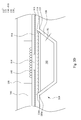
- FIG. 1A illustrates a cross-sectional view of a chip package, in accordance with some embodiments of the present disclosure.
- FIG. 1B illustrates a partial enlarge view of a region S of FIG. 1A , in accordance with some other embodiments of the present disclosure.
- FIG. 1C is a enlarge view illustrating a region S in FIG. 1A , in accordance with some embodiments of the present disclosure.
- FIG. 2 illustrates a flow chart of a method of manufacturing the chip package, in accordance with various embodiments.
- FIGS. 3A to 3H are cross-sectional views illustrating various process stages of manufacturing the chip package shown in FIG. 1A , in accordance with some embodiments.
- FIG. 4A to 4B are cross-sectional views illustrating the chip package at intermediate stages of manufacture, in accordance with some embodiments of the present disclosure.
- spatially relative terms such as “beneath”, “below”, “lower”, “above,” “upper”, and the like, are used to describe the relationship of an element shown in the drawings to another element. It should be understood that the spatially relative terms are intended to encompass different orientations of the device in addition to the orientation depicted in the figures. For example, if a device in a figure is turned over, elements originally described as being located “below” the other elements will be oriented “above” other elements. Illustrative term “below” may include both the “above” and “below” orientations according to the particular orientation of the figures.
- FIG. 1A illustrates a cross-sectional view of a chip package 100 , in accordance with some embodiments of the present disclosure.
- the chip package 100 includes a chip 110 , an insulating layer 120 , and a conductive layer 130 .
- the chip 110 includes a substrate 112 , an epitaxy layer 114 , a device region 116 and a conductive pad 118 .
- the epitaxy layer 114 is disposed on the substrate 112
- the device region 116 and the conductive pad 118 are disposed on the epitaxy layer 114 .
- the conductive pad 118 is disposed at a side of the device region 116 and in contact with the device region 116 .
- the device region 116 has a semiconductor device.
- the chip 110 may optionally include an inter-layer dielectric layer (ILD), an inter-metal dielectric layer (IMD) 115 , a passivation layer, and an interconnect metal structure, in which one or more metal layers of the interconnect metal structure extends from an interior of the device region 116 to a position out of the device region 116 to serve as the conductive pad 118 of the chip package 100 , and electrically connect to the semiconductor device of the device region 116 .
- ILD inter-layer dielectric layer
- IMD inter-metal dielectric layer
- passivation layer a passivation layer
- an interconnect metal structure in which one or more metal layers of the interconnect metal structure extends from an interior of the device region 116 to a position out of the device region 116 to serve as the conductive pad 118 of the chip package 100 , and electrically connect to the semiconductor device of the device region 116 .
- the inter-metal dielectric layer 115 laterally extends from the interior of device region 116 to a position out of the device region 116 , such that at least a portion of the inter-metal dielectric layer 115 is positioned between the epitaxy layer 114 and the conductive pad 118 .
- the substrate 112 is a blank substrate without any device.
- the materials of the substrate 112 may include, but not limited to, silicon or other semiconductor elements, such as germanium or elements of group III-V.
- the thickness of the epitaxy layer 114 is between 4 and 8 micrometer, and the crystallinity of the epitaxy layer 114 is greater than the substrate 112 .
- the materials of the epitaxy layer 114 may include, but not limited to, epitaxial silicon, epitaxial germanium or other epitaxial elements of group III-VI.
- some impurities can be doped in the epitaxy layer 114 to form an N-type epitaxy layer.
- the charges in the N-type epitaxy layer is transported by electrons which have a faster transporting speed, as compared with holes, and therefore the charge collection time can be shortened, leading to the chip package 100 with a faster responding speed.
- the chip package 100 further comprising a spacer 140 , a sensing device 145 and a transparent substrate 150 .
- the sensing device 145 is disposed on the device region 116 and substantially corresponds to the device region 116 .
- the sensing device 145 can detective incident light and generate digital signals.
- the device region 116 of the chip performs an operational process on the signals, and outputs the operational results to an external device through the conductive pad 112 .
- the spacer 140 is disposed on the device region 116 and surrounds the sensing device 145 .
- the transparent layer 150 is positioned on the spacer 140 and covers the sensing device 145 .
- the transparent layer 150 allows light to pass there through.
- the spacer 140 makes the transparent layer 150 being spaced apart from the sensing device 145 by a spacing interval.
- the spacer 140 and the transparent layer 150 collectively forming a cavity, to protect the sensing device 145 .
- the sensing device 145 includes a plurality of microlens.
- the spacer 140 includes suitable insulating material, such as epoxy resin, and examples of the materials of the transparent layer 150 include glass or other suitable transparent materials.
- the chip further includes a reflection layer 113 interposed between the substrate 112 and the epitaxy layer 114 .
- the light passing through the transparent layer 150 but not transmitting into the sensing device 145 are reflected once again by the refection layer 113 , and then arrives the sensing device 145 . Therefore, the transform of incident light signals into digital signals becomes more efficient.
- thickness of the reflection layer 113 is ranged between 1 and 2 micrometer, and the material of the reflection layer 113 includes silicon dioxide.
- FIG. 1A the conductive pad 118 is protruded out of a side surface 114 a of the epitaxy layer 114 .
- the insulating layer 120 is positioned below the substrate 112 and extends to cover the side surface 114 a of the epitaxy layer 114 .
- the conductive layer 130 is positioned below the insulating layer 120 and extends to contact the conductive pad 118 , but the conductive layer 130 dose not contact the side surface 114 a of the epitaxy layer 114 .
- FIG. 1B illustrates an enlarge view of a region S of FIG. 1A , in accordance with some other embodiments of the present disclosure. In FIG.
- the conductive layer 130 and the side surface of the epitaxy layer 114 are separated by a first distance D 1 .
- the epitaxy layer 114 can enhance operational efficiency of the chip package 100 , when external current signals are transmitted through the conductive layer 130 to the epitaxy layer 114 , an incorrect electrical connection occurs and that leads to short circuit in the chip package 100 .
- the conductive layer 130 and the epitaxy layer 114 are separated by the first distance D 1 in this disclosure, but the insulating layer 120 is interposed there between so as to secure the electrical insulation between the conductive layer 130 and epitaxy layer 114 .
- the current signals are input to or output from the conductive layer 130 only through the conductive pad 118 , and therefore the yield of the chip package 100 may be increased.
- a suitable first distance D 1 should be arranged between the conductive layer 130 and the epitaxy layer 114 .
- the first distance D 1 is greater than 6 micrometers, and specifically between 6 micrometers and 10 micrometers.
- examples of the material of the insulating layer 120 include polymeric material, which has fluidity before being cured.
- the polymeric material of the insulating layer 120 is epoxy, preferably a photosensitive epoxy.
- examples the material of the conductive layer 160 includes aluminum, copper, nickel, and any other suitable conductive materials.
- the reflection layer 113 in the chip 110 also has small conductivity.
- the side surface 113 a of the reflective layer 113 and the conductive layer 130 are separated by a second distance D 2 , and the insulating layer 120 is disposed between the conductive layer 130 and the reflective layer 113 so as to electrically insulate the reflective layer 113 from the conductive layer 130 .
- the side surface 114 a of the epitaxy layer 114 and the side surface 113 a of the reflective layer 113 are substantially coplanar, and that makes the first distance D 1 equals the second distance D 2 , but the present disclosure is not limited thereto.
- FIG. 1C illustrates an enlarged view of region S in FIG. 1A in accordance with another embodiment of the present disclosure.
- the side surface 114 a of the epitaxy layer 114 is recessed with respect to the side surface 113 a of the reflection layer 113 .
- the first distance D 1 between the conductive layer 130 and the side surface 114 a can be further increased such that the first distance D 1 is greater than the second distance D 2 .
- the polymeric material of the insulating layer 120 have fluidity before being cured, and it may flow into and fill the recess of the epitaxy layer 114 .
- the chip package further comprises a protective layer 160 and an external conductive structure 170 .
- the protective layer 160 is disposed below the conductive layer 130 to prevent external moisture from eroding the conductive layer 130 , and the protective layer 160 has an opening 162 to expose the conductive layer 130 .
- the external conductive structure 170 is disposed in the opening 162 and in contact with the conductive layer 130 . Accordingly, the external conductive structure 170 is electrically connected to the device region 116 through the conductive layer 130 and the conductive pad 118 , so that it operational signals may be transmitted to an external device, such as a printed circuit board. Alternatively, current signal provided by an external device may be transmitted to the device region 116 through the same passage.
- the material of the protective layer 160 includes epoxy, such as photosensitive epoxy.
- the external conductive structure 170 is a solder ball, a bump, or other structures known in the art, and the external conductive connection may be spherical, oval, square or rectangular in shape, but not limited thereto.
- FIG. 2 it shows a flow chart illustrating a method of manufacturing the chip package, in accordance with various embodiments.
- the method of manufacturing the chip package may be further understood with reference to FIGS. 3A to 3H .
- FIGS. 3A to 3H are cross-sectional views illustrating various process stages of manufacturing the chip package depicted in FIG. 2 .
- a wafer 300 is provided.
- the wafer 300 includes a substrate 112 , an epitaxy layer 114 , a device region 116 and a conductive pad 118 .
- the epitaxy layer 114 is positioned over the substrate 112 , and both the device region 116 and the conductive pad 118 are disposed on the epitaxy layer 114 .
- the conductive pad 118 is positioned at a side of the device region 116 and is connected to the device region 116 .
- the wafer 300 further includes a reflection layer 113 interposed between the substrate 112 and the epitaxy layer 114 .
- the wafer 300 has a plurality of chip regions, and these chip regions are diced to form a plurality of chips shown in FIG. 1A in a subsequent dicing process.
- one or more metal layers, in the interconnect metal structure of the device region 116 in the wafer 300 are connected with the semiconductor devices of device region 116 , and further extend out to serve as the conductive pad 118 .
- the inter-metal dielectric layer 115 is positioned between the epitaxy layer 114 and the conductive pad 118 .
- the wafer 300 further includes a sensing device 145 positioned above the device region 116 and substantially corresponding to the device region 116 .
- a spacer 140 is formed to surround the sensing device 145
- a transparent substrate 150 is formed above the spacer 140 and covers the sensing device 145 .
- the substrate 112 is pattered.
- a portion of the substrate 112 is removed by a photolithography-etching approach to form a recess 310 exposing the reflection layer 113 .
- Particular steps of photolithography-etching include forming a photoresist layer covering the substrate 112 , and exposing the photoresist layer by using a mask with a predetermined pattern so as to transfer the predetermined pattern onto the photoresist layer. After removing the mask, the substrate 112 where is not protected by the photoresist layer is etched by a suitable solvent or a plasma gas until the reflection layer 113 is revealed.
- a portion of the epitaxy layer 114 is removed using the patterned substrate 112 as a mask such that the inter-metal dielectric layer 115 and the conductive pad 118 protrudes out of the side surface 114 a of the epitaxy layer 114 .
- the exposed portion of the reflective layer 113 is directly etched using the patterned substrate 112 as a mask to expose the epitaxy layer 114 below the reflective layer 113 .
- the etching process continues to etch the exposed portion of the epitaxy layer 114 , and the condition of the etching process is controlled to stop at the surface of the inter-metal dielectric layer 115 Specifically, the etching firstly removes a portion of the reflection layer 113 so to expose the side surface 113 a thereof through the recess 310 , and then continuously removes a portion of the epitaxy layer 114 to expose the side surface 114 a thereof in the recess 310 , and stops at the surface of the inter-metal dielectric layer 115 . Accordingly, the conductive pad 118 may protrude out of the side surface 114 a of the epitaxy layer 114 because it is not etched in this step.
- the solvent or plasma gas used in this step has a high selectivity with respect to the reflective layer 113 and the epitaxy layer 114 , and therefore the removal of the substrate 112 may be prevented in the etching process, and the remained substrate 112 can be kept.
- an insulating layer 120 is formed below the substrate 112 , and the insulating layer 120 extends to cover the side surface 114 a of the epitaxy layer 114 and the inter-metal dielectric layer 115 .
- polymeric material is used to cover the substrate 112 . Since the polymeric material has fluidity, it may flow along the substrate 112 and cover the substrate 112 , the side surface 113 a of the reflective layer 113 , the side surface 114 a of the epitaxy layer 114 , and the surface of the inter-metal dielectric layer 115 .
- the polymeric material is a photosensitive epoxy, and an exposure is performed thereon. Therefore, the polymeric material is cross-linked and cured to form the insulating layer 120 .
- the approach of forming the insulating layer 120 includes a spin coating process a printing process, or other suitable deposition approaches, for example.
- the thickness T 1 of the insulating layer 120 at the side surface 114 a of the epitaxy layer 114 dominates the distance between the conductive layer 130 and the epitaxy layer 114 . Therefore, the thickness T 1 at the side surface of the insulating layer 120 is managed to make sure the electrical insulation between the epitaxy layer 114 and the conductive layer 130 . In some embodiments, the thickness T 1 at the side surface of the insulating layer 120 is greater than 6 micrometer, preferably between 6 and 10 micrometer.
- a notch 320 is formed in the insulating layer 120 so to expose the conductive pad 118 .
- a knife is used to cut off a portion of the insulating layer 120 , a portion of the conductive pad 118 , and a portion of the spacer 1 to form the notch 320 exposing the side surface 118 a of the conductive pad 118 .
- a conductive layer 130 is formed below the insulating layer 120 , and the conductive layer 130 is extended to the notch 320 and in contact with the side surface 118 a of the conductive pad 118 .
- a layer of conductive material may be deposited, for example, by sputtering techniques, evaporating techniques, electroplating techniques, or electroless plating, and then a photolithography-etching process is carried out to pattern the deposited conductive material layer, thereby forming the conductive layer 130 .
- the thickness T 1 of the insulating layer 120 at the side surface 114 a of the epitaxy layer 114 allows that the side surface 114 a and the conductive layer 130 are separated by a first distance D 1 to avoid incorrect electrical connections and short circuit between the conductive layer 130 and the epitaxy layer 114 , in which the thickness T 1 is substantially the same as the first distance D 1 .
- the side surface 113 a of the reflective layer 113 and the conductive layer 130 are separated by a second distance D 2 which is substantially equal to the first distance D 1 .
- materials of the conductive layer 560 includes aluminum, copper, nickel or other suitable conductive materials.
- a protective layer 160 is formed below the conductive layer 130 , and an opening 162 is formed in the protective layer 160 so as to expose the conductive layer 130 .
- the protective layer 160 may be formed to cover the conductive layer 130 by a process of brush-coating an epoxy material under the conductive layer 130 . Subsequently, the protective layer 160 is pattered to form the opening 162 so to expose a portion of the conductive layer 130 from the opening 162 of the protective layer 160 .
- the material of the protective layer 160 is a photosensitive epoxy, and therefore the protective layer 160 may be patterned directly by a photolithography process, and no additional photoresist layer is required for defining the pattern of the protective layer 160 .
- the material of the protective layer 160 is the same as that of the insulating layer 120 , but the present disclosure is not limited thereto.
- an external conductive structure 170 is formed in the opening 162 , and the wafer 300 is cut along the notch 320 to form the chip package 100 in FIG. 1A .
- the external conductive structure 170 may be a solder ball, a bump, or other structures known in the industry, and the external conductive structure 170 may be spherical, oval, square or rectangular in shape, but not limited thereto.
- the protective layer 160 , the conductive layer 130 , the spacer 140 and the transparent substrate 150 are cut along a scribe line 330 in the notch 320 to separate these chip regions of the wafer 300 , thereby forming a number of individual chip packages.
- the scribe line 330 is located within the notch 320 .
- FIG. 4A and 4B are cross-sectional views illustrating intermediate stages in a method for manufacturing a chip package, in accordance with some embodiments of the present disclosure.
- FIG. 4A illustrates a process stage after the process stage shown in FIG. 3C hereinbefore.
- the side surface 114 a of the epitaxy layer 114 is further laterally etched after the removal of the portions of the epitaxy layer 114 and reflective layer 113 .
- the side surface 114 a of the epitaxy layer 114 are initially coplanar with the side surface 113 a of the reflective layer 113 such that the first distance D 1 substantially equals the second distance D 2 .
- the side surface 114 a of the epitaxy layer 114 is recessed with respect to the side surface 113 a of the reflective layer 113 so to form a recess 410 , as shown in FIG. 4A . Therefore, it may increase the first distance D 1 between the side surface 114 a of the epitaxy layer 114 and the conductive layer formed subsequently. Further, a sufficient portion of the reflective layer 113 may be retained in the chip package such that the optical conversion efficiency of chip package can be maintained.
- the lateral etching has a relatively high etching selectivity for the epitaxy layer 114 .
- the solvent or plasma used in the etching has a high etching rate for the epitaxy layer 114 with respect to both of the reflective layer 113 and the inter-metal dielectric layer 115 .
- an insulating layer 120 is formed below the substrate 112 , and the insulating layer 120 is extended to cover the side surface 114 a of the epitaxy layer 114 and the surface of the inter-metal dielectric layer 115 .
- the polymeric material of the insulating layer 120 may cover the substrate 112 , the side surface 113 a of the reflective layer 113 , the side surface 114 a of the epitaxy layer 114 , and the surface of the inter-metal dielectric layer 115 , and further flows in and fills the recess 410 because of its fluidity.
- the approach of forming the insulating layer 120 may refer to these described hereinbefore in connection with FIG.
- the method may continue to perform the process steps shown in FIG. 3E , FIG. 3F , FIG. 3G and FIG. 3H , and eventually individual chip packages are formed.
- the first distance D 1 between the side surface 114 a of the epitaxy layer 114 and the conductive layer 130 is further increased such that the first distance D 1 is greater than the second distance D 2 between the side surface 113 a of the reflective layer 113 and the conductive layer 130 .
- the epitaxy layer of the chip package is spaced apart from the conductive layer by a distance, and the epitaxy layer is not in contact with the conductive layer.
- An insulating layer is further disposed between the epitaxy layer and the conductive layer, and therefore the epitaxy layer is insulated from the conductive pad. Accordingly, the current can not be transmitted (input/output) between the conductive layer 130 and the epitaxy layer, and the short circuit there between is prevented.
- no additional photoresist layer is required to form the conductive layer protruding out of the side surface of the epitaxy layer, and thereby the manufacturing process and cost can be reduced.
- the chip packages are manufactured in a wafer-level scale so that the manufacturing cost is lower than that of the conventional wire-bonding process.
- the diced chip packages are chip-scale packages, and it is good for the miniaturized design.
Landscapes
- Engineering & Computer Science (AREA)
- Physics & Mathematics (AREA)
- Power Engineering (AREA)
- Microelectronics & Electronic Packaging (AREA)
- Condensed Matter Physics & Semiconductors (AREA)
- General Physics & Mathematics (AREA)
- Computer Hardware Design (AREA)
- Electromagnetism (AREA)
- Manufacturing & Machinery (AREA)
- Solid State Image Pick-Up Elements (AREA)
- Internal Circuitry In Semiconductor Integrated Circuit Devices (AREA)
Priority Applications (1)
| Application Number | Priority Date | Filing Date | Title |
|---|---|---|---|
| US15/393,006 US9859320B2 (en) | 2015-12-29 | 2016-12-28 | Chip package and manufacturing method thereof |
Applications Claiming Priority (2)
| Application Number | Priority Date | Filing Date | Title |
|---|---|---|---|
| US201562272603P | 2015-12-29 | 2015-12-29 | |
| US15/393,006 US9859320B2 (en) | 2015-12-29 | 2016-12-28 | Chip package and manufacturing method thereof |
Publications (2)
| Publication Number | Publication Date |
|---|---|
| US20170186797A1 US20170186797A1 (en) | 2017-06-29 |
| US9859320B2 true US9859320B2 (en) | 2018-01-02 |
Family
ID=59087417
Family Applications (1)
| Application Number | Title | Priority Date | Filing Date |
|---|---|---|---|
| US15/393,006 Active US9859320B2 (en) | 2015-12-29 | 2016-12-28 | Chip package and manufacturing method thereof |
Country Status (3)
| Country | Link |
|---|---|
| US (1) | US9859320B2 (zh) |
| CN (1) | CN106935558A (zh) |
| TW (1) | TWI630712B (zh) |
Families Citing this family (2)
| Publication number | Priority date | Publication date | Assignee | Title |
|---|---|---|---|---|
| TWI744163B (zh) * | 2020-01-06 | 2021-10-21 | 精材科技股份有限公司 | 晶片封裝體及其製造方法 |
| US11695199B2 (en) * | 2020-08-25 | 2023-07-04 | Xintec Inc. | Antenna device and manufacturing method thereof |
Citations (1)
| Publication number | Priority date | Publication date | Assignee | Title |
|---|---|---|---|---|
| US20130214375A1 (en) * | 2012-02-16 | 2013-08-22 | Omnivision Technologies, Inc. | Pad and circuit layout for semiconductor devices |
Family Cites Families (8)
| Publication number | Priority date | Publication date | Assignee | Title |
|---|---|---|---|---|
| US7528420B2 (en) * | 2007-05-23 | 2009-05-05 | Visera Technologies Company Limited | Image sensing devices and methods for fabricating the same |
| TWI395346B (zh) * | 2008-05-23 | 2013-05-01 | Xintec Inc | 發光元件的封裝結構 |
| JP5356742B2 (ja) * | 2008-07-10 | 2013-12-04 | ラピスセミコンダクタ株式会社 | 半導体装置、半導体装置の製造方法および半導体パッケージの製造方法 |
| TWI511243B (zh) * | 2009-12-31 | 2015-12-01 | Xintec Inc | 晶片封裝體及其製造方法 |
| US8432032B2 (en) * | 2010-01-13 | 2013-04-30 | Chia-Sheng Lin | Chip package and fabrication method thereof |
| TWI525758B (zh) * | 2010-01-21 | 2016-03-11 | 精材科技股份有限公司 | 晶片封裝體及其製造方法 |
| US9768223B2 (en) * | 2011-12-21 | 2017-09-19 | Xintec Inc. | Electronics device package and fabrication method thereof |
| KR102171024B1 (ko) * | 2014-06-16 | 2020-10-29 | 삼성전자주식회사 | 반도체 발광소자 패키지의 제조 방법 |
-
2016
- 2016-12-28 CN CN201611234243.7A patent/CN106935558A/zh not_active Withdrawn
- 2016-12-28 US US15/393,006 patent/US9859320B2/en active Active
- 2016-12-28 TW TW105143683A patent/TWI630712B/zh active
Patent Citations (1)
| Publication number | Priority date | Publication date | Assignee | Title |
|---|---|---|---|---|
| US20130214375A1 (en) * | 2012-02-16 | 2013-08-22 | Omnivision Technologies, Inc. | Pad and circuit layout for semiconductor devices |
Also Published As
| Publication number | Publication date |
|---|---|
| TWI630712B (zh) | 2018-07-21 |
| US20170186797A1 (en) | 2017-06-29 |
| CN106935558A (zh) | 2017-07-07 |
| TW201740548A (zh) | 2017-11-16 |
Similar Documents
| Publication | Publication Date | Title |
|---|---|---|
| US10157811B2 (en) | Chip package and method for forming the same | |
| US9196754B2 (en) | Chip package and fabrication method thereof | |
| US8564101B2 (en) | Semiconductor apparatus having a through-hole interconnection | |
| US9502455B2 (en) | Optical apparatus having resin encased stacked optical and semiconductor devices | |
| US9337097B2 (en) | Chip package and method for forming the same | |
| US9177919B2 (en) | Chip package and method for forming the same | |
| US9768223B2 (en) | Electronics device package and fabrication method thereof | |
| US9768089B2 (en) | Wafer stack protection seal | |
| US20150255499A1 (en) | Chip package and method of fabricating the same | |
| US20120184070A1 (en) | Method for forming chip package | |
| US8810012B2 (en) | Chip package, method for forming the same, and package wafer | |
| CN103715108A (zh) | 半导体装置和将密封剂沉积在嵌入式wlcsp中的方法 | |
| US9362134B2 (en) | Chip package and fabrication method thereof | |
| CN110943052B (zh) | 晶片封装体及其制造方法 | |
| US8786093B2 (en) | Chip package and method for forming the same | |
| US20170207194A1 (en) | Chip package and method for forming the same | |
| TWI540655B (zh) | 半導體結構及其製造方法 | |
| US20160355393A1 (en) | Chip package and manufacturing method thereof | |
| US9799778B2 (en) | Chip package having a trench exposed protruding conductive pad | |
| CN107369695B (zh) | 晶片封装体与其制造方法 | |
| US9859320B2 (en) | Chip package and manufacturing method thereof | |
| US9865526B2 (en) | Chip package and method for forming the same | |
| US9269732B2 (en) | Chip package | |
| US20130341739A1 (en) | Package structure having micro-electro-mechanical system element and method of fabrication the same | |
| US10665538B2 (en) | Semiconductor device |
Legal Events
| Date | Code | Title | Description |
|---|---|---|---|
| AS | Assignment |
Owner name: XINTEC INC., TAIWAN Free format text: ASSIGNMENT OF ASSIGNORS INTEREST;ASSIGNORS:LONG, SHUN-WEN;CHIOU, GUO-JYUN;KUO, MENG-HAN;AND OTHERS;REEL/FRAME:040791/0106 Effective date: 20161226 |
|
| STCF | Information on status: patent grant |
Free format text: PATENTED CASE |
|
| MAFP | Maintenance fee payment |
Free format text: PAYMENT OF MAINTENANCE FEE, 4TH YEAR, LARGE ENTITY (ORIGINAL EVENT CODE: M1551); ENTITY STATUS OF PATENT OWNER: LARGE ENTITY Year of fee payment: 4 |