US9829794B2 - Exposure apparatus, and method of manufacturing device - Google Patents
Exposure apparatus, and method of manufacturing device Download PDFInfo
- Publication number
- US9829794B2 US9829794B2 US14/994,686 US201614994686A US9829794B2 US 9829794 B2 US9829794 B2 US 9829794B2 US 201614994686 A US201614994686 A US 201614994686A US 9829794 B2 US9829794 B2 US 9829794B2
- Authority
- US
- United States
- Prior art keywords
- substrate
- exposure
- optical system
- light
- peripheral portion
- Prior art date
- Legal status (The legal status is an assumption and is not a legal conclusion. Google has not performed a legal analysis and makes no representation as to the accuracy of the status listed.)
- Active
Links
Images


Classifications
-
- G—PHYSICS
- G03—PHOTOGRAPHY; CINEMATOGRAPHY; ANALOGOUS TECHNIQUES USING WAVES OTHER THAN OPTICAL WAVES; ELECTROGRAPHY; HOLOGRAPHY
- G03F—PHOTOMECHANICAL PRODUCTION OF TEXTURED OR PATTERNED SURFACES, e.g. FOR PRINTING, FOR PROCESSING OF SEMICONDUCTOR DEVICES; MATERIALS THEREFOR; ORIGINALS THEREFOR; APPARATUS SPECIALLY ADAPTED THEREFOR
- G03F7/00—Photomechanical, e.g. photolithographic, production of textured or patterned surfaces, e.g. printing surfaces; Materials therefor, e.g. comprising photoresists; Apparatus specially adapted therefor
- G03F7/70—Microphotolithographic exposure; Apparatus therefor
- G03F7/70483—Information management; Active and passive control; Testing; Wafer monitoring, e.g. pattern monitoring
-
- G—PHYSICS
- G03—PHOTOGRAPHY; CINEMATOGRAPHY; ANALOGOUS TECHNIQUES USING WAVES OTHER THAN OPTICAL WAVES; ELECTROGRAPHY; HOLOGRAPHY
- G03F—PHOTOMECHANICAL PRODUCTION OF TEXTURED OR PATTERNED SURFACES, e.g. FOR PRINTING, FOR PROCESSING OF SEMICONDUCTOR DEVICES; MATERIALS THEREFOR; ORIGINALS THEREFOR; APPARATUS SPECIALLY ADAPTED THEREFOR
- G03F7/00—Photomechanical, e.g. photolithographic, production of textured or patterned surfaces, e.g. printing surfaces; Materials therefor, e.g. comprising photoresists; Apparatus specially adapted therefor
- G03F7/20—Exposure; Apparatus therefor
- G03F7/2022—Multi-step exposure, e.g. hybrid; backside exposure; blanket exposure, e.g. for image reversal; edge exposure, e.g. for edge bead removal; corrective exposure
- G03F7/2026—Multi-step exposure, e.g. hybrid; backside exposure; blanket exposure, e.g. for image reversal; edge exposure, e.g. for edge bead removal; corrective exposure for the removal of unwanted material, e.g. image or background correction
- G03F7/2028—Multi-step exposure, e.g. hybrid; backside exposure; blanket exposure, e.g. for image reversal; edge exposure, e.g. for edge bead removal; corrective exposure for the removal of unwanted material, e.g. image or background correction of an edge bead on wafers
-
- G—PHYSICS
- G03—PHOTOGRAPHY; CINEMATOGRAPHY; ANALOGOUS TECHNIQUES USING WAVES OTHER THAN OPTICAL WAVES; ELECTROGRAPHY; HOLOGRAPHY
- G03F—PHOTOMECHANICAL PRODUCTION OF TEXTURED OR PATTERNED SURFACES, e.g. FOR PRINTING, FOR PROCESSING OF SEMICONDUCTOR DEVICES; MATERIALS THEREFOR; ORIGINALS THEREFOR; APPARATUS SPECIALLY ADAPTED THEREFOR
- G03F7/00—Photomechanical, e.g. photolithographic, production of textured or patterned surfaces, e.g. printing surfaces; Materials therefor, e.g. comprising photoresists; Apparatus specially adapted therefor
- G03F7/70—Microphotolithographic exposure; Apparatus therefor
- G03F7/70691—Handling of masks or workpieces
- G03F7/70716—Stages
- G03F7/70725—Stages control
Definitions
- the present invention relates to an exposure apparatus, and a method of manufacturing a device.
- a resist photosensitive agent
- the resist is peeled off, for example, during substrate transfer, which may cause a defect of the semiconductor devices.
- the resist of the peripheral portion of the substrate is exposed (peripheral exposure) using an exposure apparatus (a so-called peripheral exposure apparatus), and the resist is removed in a subsequent developing process.
- an exposure apparatus a so-called peripheral exposure apparatus
- Japanese Patent Laid-Open No. 9-260263 discloses a peripheral exposure apparatus that performs focus adjustment by detecting a change in a relative distance between a peripheral exposure means and a resist coating surface of the substrate, and by performing the driving of the focusing direction of the peripheral exposure means based on the detected relative distance.
- the present invention provides, for example, an exposure apparatus that is advantageous in accuracy of a portion of a substrate exposed by peripheral exposure thereof to light.
- the present invention has an exposure apparatus that exposes a peripheral portion of a substrate to light.
- the apparatus comprising: an optical system configured to irradiate the substrate with the light; a stage configured to hold the substrate and be moved in a direction to position the substrate in a direction perpendicular to an optical axis of the optical system; and a controller configured to cause the stage to be moved, wherein the controller is configured to cause the stage to be moved based on information about a distance between the optical system and the peripheral portion in a direction parallel to the optical axis and a telecentricity of the optical system so that a predetermined portion of the substrate is irradiated with the light from the optical system.
- FIG. 1 is a diagram illustrating a configuration of an exposure apparatus according to a first embodiment.
- FIG. 2A is a diagram illustrating a state at the time of a peripheral exposure in the first embodiment.
- FIG. 2B is a diagram illustrating a state at the time of the peripheral exposure in the first embodiment.
- FIG. 3 is a flow chart illustrating the flow of the peripheral exposure in the first embodiment.
- FIG. 4A is a diagram illustrating a configuration of an exposure apparatus according to a second embodiment.
- FIG. 4B is a diagram illustrating the configuration of the exposure apparatus according to the second embodiment.
- FIG. 5 is a flowchart illustrating the flow of the peripheral exposure in the second embodiment.
- FIG. 6 is a diagram illustrating a configuration of an exposure apparatus according to a third embodiment.
- FIG. 7A is a diagram illustrating a state at the time of the peripheral exposure in the third embodiment.
- FIG. 7B is a diagram illustrating a state at the time of the peripheral exposure in the third embodiment.
- FIG. 8 is a flowchart illustrating the flow of the peripheral exposure in the third embodiment.
- FIG. 9 is a diagram illustrating a configuration of an exposure apparatus according to a fourth embodiment.
- FIG. 10 is a flowchart illustrating the flow of the peripheral exposure in the fourth embodiment.
- FIG. 11 is a diagram illustrating a configuration of an exposure system according to an embodiment.
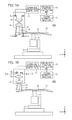
- FIG. 1 is a schematic cross-sectional view illustrating a configuration of an exposure apparatus 100 according to this embodiment.
- the exposure apparatus 100 has a stage S including a substrate holder 1 , a rotary driving unit 2 and a translational driving unit 3 , a detector 4 , an exposure unit 5 , and a control system 20 . Further, in each drawing below FIG.
- an X-axis and a Y-axis in a direction perpendicular to the X-axis are defined in a plane perpendicular to a Z-axis in a vertical direction.
- the substrate W is, for example, made of monocrystalline silicon, and is a substrate to be processed on which the resist is applied to the surface.
- the substrate holder 1 holds a substantially central position of a rear surface of the substrate W.
- the rotary driving unit (rotary unit) 2 supports the substrate holder 1 and is rotatable.
- the translational driving unit 3 supports the rotary driving unit 2 and is, for example, movable in the X-axis direction, that is, allows the substrate holder 1 to move in the X-axis direction.
- the detector 4 detects the position of the peripheral portion of the substrate W held by the substrate holder 1 , for example, a position of a notch or an orientation flat that is previously formed on the substrate W.
- the exposure unit 5 includes a light source (not illustrated), a driving slit 6 and an exposure optical system (an optical system) 18 .
- the light source emits light (e.g., ultraviolet light) toward the exposure optical system 18 .
- the driving slit (a member of a field stop) 6 has an opening through which light emitted from the light source passes to define an exposure region, and its opening shape (an opening width) is variable.
- the exposure optical system 18 irradiates (images) a predetermined position on the substrate W using the light passing through the opening of the driving slit 6 as the exposure light.
- the control system (a controller) 20 performs the control of the operation of each element constituting the exposure apparatus 100 (the movement operation of the substrate holder 1 , the driving operation of the driving slit 6 and the like), and the arithmetic operations for the operation, and includes an input unit and a control circuit as follows.
- Information about conditions of the peripheral exposure, such as an exposure amount, an exposure position or an exposure width is received by (input to) a first information input unit 9 from the outside.
- Information (distance information D) about a distance between the substrate W held by the substrate holder 1 and the exposure optical system 18 in the direction parallel to the optical axis of the exposure optical system 18 is received by (input to) a second information input unit 12 from the outside.
- a driving condition calculation unit 8 calculates the rotational speed of the rotary driving unit 2 at the time of the peripheral exposure based on the exposure amount obtained from the first information input unit 9 . Further, the driving condition calculation unit 8 calculates the position in the X-axis direction of the substrate W at the time of the peripheral exposure based on the exposure position obtained from the first information input unit 9 . The driving condition calculation unit 8 may calculate the position in the X-axis direction of the substrate W to adjust the deviation of the center position of the substrate W in the X-Y plane obtained by the detection using the detector 4 .
- the driving condition calculation unit 8 obtains an azimuth angle ⁇ of the substrate W held by the substrate holder 1 W based on a reference position in an azimuth angle direction of the substrate W, such as a notch or an orientation flat detected by the detector 4 . Furthermore, the driving condition calculation unit 8 calculates the position in the X-axis direction of the translational driving unit 3 based on the distance information D obtained from the second information input unit 12 . The driving slit condition calculation unit 10 calculates an opening width set in the driving slit 6 based on the exposure width obtained from the first information input unit 9 .
- An X ⁇ controller 7 drives the rotary driving unit 2 an amount of movement (driving amount) at which the substrate W is located at the position in the X-axis direction determined by the driving condition calculation unit 8 .
- the driving slit opening width controller 11 drives the driving slit 6 to an opening width determined by the driving slit condition calculation unit 10 .
- the exposure unit 5 irradiates a part of the peripheral portion of the substrate W with the exposure light while the X ⁇ controller 7 rotates the rotary driving unit (rotation device) 2 at a desired rotational speed, and thus the exposure apparatus 100 can expose the entire peripheral portion of the substrate W at a set exposure position or a set exposure width.
- the X ⁇ controller 7 rotates the rotary driving unit (rotation device) 2 at a desired rotational speed, and thus the exposure apparatus 100 can expose the entire peripheral portion of the substrate W at a set exposure position or a set exposure width.
- the shape of the substrate W is not flat and especially when the peripheral portion is warped, or when the thickness is uneven, if the peripheral exposure is performed without taking any precautions, there is a possibility of the following inconvenience.
- FIGS. 2A and 2B are schematic cross-sectional views illustrating a state of the exposure apparatus 100 when the peripheral exposure of the substrate W is performed while a peripheral portion is warped toward a vertically lower side.
- FIG. 2A illustrates a state prior to offsetting the position of the substrate W.
- the exposed surface on the substrate W is defocused from an ideal imaging surface 15 illustrated by a two-dot chain line.
- a general peripheral exposure apparatus is designed so that the main light beam 13 of the exposure optical system is perpendicular to the ideal imaging surface 15 , in other words, parallel to the optical axis of the exposure optical system.
- the main light beam of the exposure optical system is not perpendicular to the ideal imaging surface 15 due to manufacturing errors or assembly errors, and for example, as illustrated by the main light beam 14 in the drawings, the on-axis main light beam and the off-axis main light beam are inclined in the same direction. Therefore, when the peripheral exposure of the substrate W is performed while the main light beam is inclined without applying the present embodiment, the main light beam is exposed to a position 17 deviated by an amount ⁇ p determined by the defocus amount and the amount of inclination of the main beam with respect to the ideal exposure position 16 . Therefore, in this embodiment, the exposure apparatus 100 performs the peripheral exposure after adjusting the position of the substrate W (the exposure position relative to the substrate W), that is, after offsetting the position of the substrate W by the amount of deviation ⁇ p of the exposure position as follows.
- FIG. 3 is a flowchart illustrating the flow of the peripheral exposure in the present embodiment.
- the second information input unit 12 acquires distance information D about the distance between the substrate W held by the substrate holder 1 and the exposure optical system 18 (step S 101 ).
- the distance information D includes at least one of the warp amount and the thickness of the substrate W, and before the substrate W is held by the substrate holder 1 , the information is measured in advance using a measuring device (measuring unit) (not illustrated). Further, the measuring device may be included or may not be included as a component of the exposure apparatus 100 .
- the measuring device configured to measure the distance between the substrate W held by the substrate holder 1 and the exposure optical system 18 may be installed inside the exposure apparatus 100 , and the results measured by the measuring device may be directly input to the second information input unit 12 .
- the measuring device can also be used in combination with the detector 4 .
- the second information input unit 12 can acquire as accurate distance information D as possible.
- the timing (timing of executing step S 101 ) of acquiring the distance information D may be provided for each substrate W, may be provided for each lot including a plurality of substrates W, or may be provided for each process.
- the driving condition calculation unit 8 acquires the amount of inclination of the main light beam 14 of the exposure optical system 18 (step S 102 ).
- the amount of inclination of the main light beam 14 is an amount of inclination of the on-axis main beam or the off-axis main beam to the ideal main light beam 13 (the optical axis of the exposure optical system 18 ), and may be telecentricity.
- the telecentricity also includes an amount of inclination (an amount of spread) when there is spreading with respect to the optical axis of the exposure optical system 18 , as in a main light beam 19 referred to in the following third embodiment, as well as the amount of inclination when the on-axis main light beam and the off-axis main light beam are inclined in parallel in the same direction.
- the amount of inclination of the main light beam 14 is obtained in advance, for example, by performing the peripheral exposure of the substrates W having the different thicknesses, and by measuring a change in position of the peripheral exposure for each thickness of the substrate W using an inspecting device (inspection unit) (not illustrated).
- the driving condition calculation unit 8 calculates the amount of deviation ⁇ p of the exposure position based on the distance information D obtained in step S 101 and the amount of inclination of the main light beam 14 of the exposure optical system 18 (step S 103 ).
- ⁇ an inclination angle of the main light beam 14 with respect to the ideal imaging surface 15
- d an amount of deviation (defocus amount) of the position in the focusing direction (in this case, the Z-axis direction) of the substrate W from the ideal imaging surface 15
- the driving condition calculation unit 8 further calculates the position in the X-axis direction of the substrate W to adjust the amount of deviation ⁇ p of the exposure position (step S 104 ).
- the X ⁇ controller 7 drives the translational driving unit 3 , and moves the rotary driving unit 2 to a position in the X-axis direction determined in step S 104 (step S 105 ). In this way, the movement of the rotary driving unit 2 only in the X-axis direction reduces the influence of telecentricity, and one positioned in the Y-axis direction in advance is assumed.
- the X-axis direction is an example, and it may be any direction in a radial direction of the substrate W.
- an exposure controller (not illustrated) irradiates the exposure unit 5 with the exposure light, while the X ⁇ controller 7 drives the rotary driving unit 2 to rotate the substrate W on the substrate holder 1 at a desired rotational speed, thereby performing the peripheral exposure (step S 106 ).
- FIG. 2B illustrates a state when the peripheral exposure is performed the position of the substrate W offset by ⁇ p.
- the exposure apparatus 100 does not require a driving unit for moving the substrate W held by the substrate holder 1 in the focusing direction (Z-axis direction) when the position of the substrate W is offset. Therefore, the exposure apparatus 100 can have a simple configuration.
- the exposure apparatus 100 can also be applied to a case in which the peripheral portion of the substrate W is warped upward. Furthermore, as factors in which the position in the focusing direction of the surface to be exposed on the substrate W is deviated from the ideal imaging surface 15 , since the thickness of the substrate W is also included without being limited to the warp of the substrate W, the exposure apparatus 100 is also applicable to the substrate W in which the thickness locally changes.
- the exposure apparatus according to this embodiment is characterized in that the distance information D( ⁇ ) for each azimuth angle ⁇ of the substrate W is provided instead of the distance information D in the first embodiment, and the peripheral exposure is performed while the offset amount ⁇ p( ⁇ ) of the substrate W is changed according to the distance information D( ⁇ ) depending on the azimuth angle ⁇ .
- FIGS. 4A and 4B are schematic cross-sectional views illustrating the configuration of the exposure apparatus 200 according to this embodiment, and a state of the exposure apparatus 200 when the peripheral exposure of the substrate W is performed while the peripheral portion is warped toward the vertically lower side.
- FIG. 4A illustrates a state when an azimuth angle of the substrate W is ⁇ 1 , and the position of the substrate W is offset by ⁇ p( ⁇ 1 ) to perform the peripheral exposure.
- FIG. 4B illustrates a state when the azimuth angle of the substrate W is ⁇ 2 , and the position of the substrate W is offset by ⁇ p( ⁇ 2 ) to perform the peripheral exposure.
- the exposure apparatus 200 performs the peripheral exposure, by offsetting the position of the substrate W in the case illustrated in FIG. 4A more significantly than in the case illustrated in FIG. 4B .
- FIG. 5 is a flowchart illustrating the flow of the peripheral exposure in the present embodiment.
- the second information input unit 12 acquires distance information D( ⁇ ) about the distance between the substrate W held by the substrate holder 1 and the exposure optical system 18 , for each azimuth angle ⁇ of the substrate W (step S 201 ).
- the driving condition calculation unit 8 acquires the amount of inclination of the main light beam 14 of the exposure optical system 18 (step S 202 ).
- the driving condition calculation unit 8 further calculates the position in the X-axis direction of the substrate W to adjust the amount of deviation ⁇ p of the exposure position for each azimuth angle ⁇ of the substrate (step S 204 ).
- the X ⁇ controller 7 rotates the substrate W at a desired rotational speed by driving the rotary driving unit 2 , and at the same time, the peripheral exposure is performed while the translational driving unit 3 is driven to the position in the X-axis direction determined in step S 204 for each azimuth angle ⁇ of the substrate W (step S 205 ).
- the means for adjusting the exposure position is not limited thereto.
- the driving slit 6 may be moved in the X-axis direction while the opening width is maintained (in the case of the configuration in which the driving slit 6 includes a plurality of blades with which the opening width is variable, a constant interval is maintained between the plurality of blades).
- the exposure apparatus according to this embodiment is characterized in that the peripheral exposure is performed after changing the opening width of the driving slit (adjustment unit) 6 depending on the distance information D referred to in the first embodiment.
- FIG. 6 is a schematic cross-sectional view illustrating a configuration of an exposure apparatus 300 according to this embodiment.
- FIGS. 7A and 7B are schematic cross-sectional views illustrating a state of the exposure apparatus 300 when the peripheral exposing of the substrate W is performed while the peripheral portion is warped toward the vertically lower side.
- FIG. 7A illustrates a state before the offset of the opening width of the driving slit 6 .
- FIG. 7B illustrates a state after the offset of the opening width of the driving slit 6 .
- the same configurations as those of the exposure apparatus 100 according to the first embodiment illustrated in FIGS. 1, 2A and 2B are denoted by the same reference numerals, and the description thereof will be omitted.
- the main light beam of the actual exposure optical system is not perpendicular to the ideal imaging surface 15 , due to a manufacturing error or an assembly error as described above.
- the exposure width of the peripheral exposure changes to spread with respect to the optical axis of the exposure optical system 18 , the exposure is performed at a position deviated by ⁇ w from a predetermined exposure position.
- the driving slit condition calculation unit 10 calculates the amount of deviation ⁇ w of the exposure width based on the distance information D, and the driving slit opening width controller 11 controls the opening width of the driving slit 6 so that the exposure width on the surface of the substrate W is offset by ⁇ w at the time of the peripheral exposure.
- the offset amount of the opening width of the driving slit 6 is (amount of deviation ⁇ w of the exposure width on the surface of the substrate W)/(magnification ⁇ of the exposure optical system 18 ).
- FIG. 8 is a flowchart illustrating the flow of the peripheral exposure in the present embodiment.
- step S 301 is identical to step S 101 of FIG. 3 in the first embodiment.
- the driving condition calculation unit 8 acquires an amount of inclination (an amount of spread) of the main light beam 19 of the exposure optical system 18 (step S 302 ).
- the driving slit condition calculation unit 10 calculates the amount of deviation ⁇ w of the exposure width based on the distance information D obtained in step S 301 and the amount of inclination of the main light beam 19 of the exposure optical system 18 (step S 303 ).
- the driving slit condition calculation unit 10 calculates the opening width to adjust the amount of deviation ⁇ w of the exposure width (step S 304 ).
- the driving slit opening width controller 11 drives the driving slit 6 to an opening width determined in step S 304 (step S 305 ).
- the X ⁇ controller 7 drives the rotary driving unit 2 to rotate the substrate W on the substrate holder 1 at a desired rotational speed, the peripheral exposure is performed (step S 306 ).
- a means of changing the opening width of the driving slit 6 is adopted as the means for adjusting the exposure width
- a means of changing the magnification ⁇ of the exposure optical system 18 by moving a part of the optical element constituting the exposure optical system 18 in the optical axis direction may be adopted.
- an amount of deviation ⁇ w( ⁇ ) may be determined for each azimuth angle ⁇ of the substrate W, and the peripheral exposure may be performed with the opening width ⁇ w( ⁇ )/ ⁇ of the driving slit 6 offset.
- the exposure apparatus according to this embodiment is characterized in that the opening width of the driving slit (adjustment unit) 6 is more complexly changed depending on the distance information D to improve upon the third embodiment.
- FIG. 9 is a schematic cross-sectional view illustrating a configuration of an exposure apparatus 400 of the present embodiment, and a state of the exposure apparatus 400 when the peripheral exposure of the substrate W is performed while the peripheral portion is warped toward the vertically lower side.
- the same configurations as those of the exposure apparatus 100 according to the first embodiment illustrated FIGS. 1, 2A and FIG. 2B are denoted by the same reference numerals, and the description thereof will be omitted.
- the driving slit 6 includes a plurality (two in this embodiment) of blades 6 a and 6 b that form an opening interposed from both sides in the X-axis direction and are movable by different amounts of movement (amounts of drive) from each other by driving of the driving unit.
- the exposure apparatus 300 determines each of the offset amount ( ⁇ w 1 / ⁇ ) of the blade 6 a and the offset amount ( ⁇ w 2 / ⁇ ) of the blade 6 b , and suitably changes the amount of offset for each of the blades 6 a and 6 b to perform the peripheral exposure.
- FIG. 10 is a flowchart illustrating the flow of the peripheral exposure in the present embodiment.
- the second information input unit 12 acquires the distance information D about the distance in the radial distances X 1 and X 2 of the substrate W between the substrate W held by the substrate holder 1 and the exposure optical system 18 (step S 401 ).
- the driving condition calculation unit 8 acquires an amount of inclination of the main light beam 19 of the exposure optical system 18 (step S 402 ).
- the driving slit opening width controller 11 drives the respective blades 6 a and 6 b to the positions calculated in step S 404 (step S 405 ). Further, while the X ⁇ controller 7 drives the rotary driving unit 2 to rotate the substrate W on the substrate holder 1 at a desired rotation speed, the peripheral exposure is performed (step S 406 ).
- the distance information D including the warp amount and the thickness of the substrate W is set as values obtained by the actual measurement.
- the distance information D that is acquired by the second information input unit 12 in step S 101 or the like and is used in the subsequent process may be classified into a plurality of degrees between the substrate W and the exposure optical system 18 depending on the magnitude.
- the degrees for example, there is a warp amount of the substrate W that can be recognized in advance due to the process, and this can be classified into several degrees such as “large,” “medium” and “small.” If the degree is “large,” the driving condition calculation unit 8 and the driving slit condition calculation unit 10 may determine the offset amount depending on the degree of “large” and may offset the substrate holder 1 and the driving slit 6 .
- the offset amounts of the exposure position or the exposure width were determined to adjust the deviation of the exposure position due to the amount of defocus (warp amount or the like) of the substrate W and the amount of inclination (telecentricity) of the main light beam.
- the offset amount is not limited to this determination method, and for example, it may be determined in consideration of a blurring width of a boundary of the exposure region due to defocus.
- the blurring width refers to a radial width of a blurred region that is generated at the boundary between an irradiation region of the exposure light and a non-irradiation region of the exposure light by the defocus.
- the driving condition calculation unit 8 acquires the number of openings NA of the exposure optical system 18 stored in a memory or the like in advance.
- FIG. 11 is a schematic diagram illustrating a configuration of an exposure system 500 according to this embodiment.
- the exposure system 500 for example, is used in a lithography process in the manufacturing process of the semiconductor device, and is a projection exposure apparatus that exposes (transfers) an image of a pattern formed on an original R onto the substrate W (on the substrate) in a step-and-repeat method.
- the exposure system 500 includes an illumination system 90 , an original stage 80 , a projection optical system 70 and a substrate stage 21 .
- the illumination system 90 adjusts the light emitted from a light source (not illustrated) to illuminate the original (reticle) R.
- the original (reticle) R is, for example, made of quartz glass, and is formed with a pattern (e.g., a circuit pattern) to be transferred onto the substrate W.
- the original stage 80 holds the original R and is movable in each of the X- and Y-axis directions.
- the projection optical system 70 projects the light passing through the original R onto the substrate W at a predetermined magnification (e.g., 1 ⁇ 2).
- the substrate stage 21 holds the substrate and is movable in each of the W and X-, Y- and Z-axis directions.
- the exposure system 500 includes two types of alignment units including a first alignment unit 600 and a second alignment unit 700 . Furthermore, the exposure system 500 includes a first carrying mechanism 50 which carries the substrate W from an interface 40 , such as a line or a FOUP, to the first alignment unit 600 , and a second carrying mechanism 60 that carries the substrate W from the first alignment unit 600 to the second alignment unit 700 .
- a first carrying mechanism 50 which carries the substrate W from an interface 40 , such as a line or a FOUP, to the first alignment unit 600
- a second carrying mechanism 60 that carries the substrate W from the first alignment unit 600 to the second alignment unit 700 .
- the first alignment unit 600 performs so-called pre-alignment of aligning the position of the substrate W to a desired position with precision that is coarser than precision of the positioning (alignment) performed by the second alignment unit 700 .
- an exposure apparatus a peripheral exposure apparatus
- the first alignment unit 600 includes a control system 20 as a first controller including an image processing unit, a rotary driving unit 2 and a translational driving unit 3 as the first driving unit, a detector 4 as a first detection unit, and an exposure unit 5 .
- the control system 20 causes the detector 4 to detect the shape of the substrate W, performs the image processing on the detection result, and causes the rotary driving unit 2 and the translational driving unit 3 to appropriately change the attitude of the substrate W based on the image processing result to a desired position.
- the second alignment unit 700 performs the alignment that matches an irradiation region irradiated with the exposure light emitted from the projection optical system 70 , and a pattern region (a shot region) set on the substrate W in advance. Specifically, the second alignment unit 700 detects and matches marks (alignment marks) 31 formed on the substrate W in advance with precision finer than the positioning precision of the first alignment unit 600 .
- the second alignment unit 700 includes a second controller 24 , a second detection unit 22 and an image processing unit 23 , in addition to the substrate stage 21 as the second driving unit.
- the second detection unit 22 is, for example, an alignment scope which detects the marks 31 .
- the second controller 24 causes the second detection unit 22 to detect the marks 31 , causes the image processing unit 23 to perform the image-processing on the detection result, and causes the substrate stage 21 to appropriately change the position of the substrate W based on the image processing result to a desired position.
- the exposure system 500 has a controller 30 .
- the controller 30 for example, is constituted by a computer or the like, is connected to each component of the exposure system 500 via a line, and can control the operation and the adjustment of each component according to a program or the like.
- the controller 30 is electrically connected to each of the control system 20 and the second controller 24 via communication lines, controls the operation of the first alignment unit 600 and the second alignment unit 700 , and receives each detection result.
- the controller 30 may be configured integrally with other parts of the exposure system 500 (within a common casing), and may be configured separately from other parts of the exposure system 500 (within a separate casing).
- the exposure system 500 performs positioning twice with the first alignment unit 600 and the second alignment unit 700 before the exposure is initiated.
- the first carrying mechanism 50 carries the substrate W carried in from the interface 40 to the first alignment unit 600 , and the first alignment unit 600 performs the pre-alignment of the wafer W as a target.
- the second carrying mechanism 60 carries the substrate W, on which the pre-alignment is completed by the first alignment unit 600 , to the substrate stage 21 as a component of the second alignment unit 700 .
- the second alignment unit 700 performs the alignment of the wafer W as a target.
- the exposure system 500 performs the pattern exposure on the substrate W on which the alignment is completed.
- the entire system can have a simple configuration. Further, according to the exposure system 500 , in the first alignment unit 600 , since the occurrence of deviation of the exposure position in the peripheral portion of the substrate W is suppressed and the peripheral exposure can be accurately performed, it is possible to suppress undesirable effects on the patterns formed on the substrate W.
- a method of manufacturing devices is suitable for manufacturing an article such as a microdevice (for example, a liquid crystal display device) or an element having a microstructure.
- This manufacturing method can include a step of forming a latent image pattern on a photosensitive agent of a substrate onto which the photosensitive agent is applied by using the above-described exposure system (step of exposing on the substrate), and a step of developing the substrate on which the latent image pattern is formed. Further, this manufacturing method includes other well-known steps (for example, oxidization, deposition, vapor deposition, doping, planarization, etching, resist removal, dicing, bonding, packaging and the like).
- the method of manufacturing devices according to the embodiment is superior to a conventional method in at least one of the performance, quality, productivity, and production cost of the article.
Applications Claiming Priority (2)
| Application Number | Priority Date | Filing Date | Title |
|---|---|---|---|
| JP2015007122A JP6661270B2 (ja) | 2015-01-16 | 2015-01-16 | 露光装置、露光システム、および物品の製造方法 |
| JP2015-007122 | 2015-01-16 |
Publications (2)
| Publication Number | Publication Date |
|---|---|
| US20160209763A1 US20160209763A1 (en) | 2016-07-21 |
| US9829794B2 true US9829794B2 (en) | 2017-11-28 |
Family
ID=56407787
Family Applications (1)
| Application Number | Title | Priority Date | Filing Date |
|---|---|---|---|
| US14/994,686 Active US9829794B2 (en) | 2015-01-16 | 2016-01-13 | Exposure apparatus, and method of manufacturing device |
Country Status (5)
| Country | Link |
|---|---|
| US (1) | US9829794B2 (zh) |
| JP (1) | JP6661270B2 (zh) |
| KR (1) | KR101988084B1 (zh) |
| CN (1) | CN105807576B (zh) |
| TW (1) | TWI604278B (zh) |
Families Citing this family (8)
| Publication number | Priority date | Publication date | Assignee | Title |
|---|---|---|---|---|
| JP6444909B2 (ja) * | 2016-02-22 | 2018-12-26 | 東京エレクトロン株式会社 | 基板処理方法、基板処理装置及びコンピュータ読み取り可能な記録媒体 |
| CN108803245B (zh) * | 2017-04-28 | 2020-04-10 | 上海微电子装备(集团)股份有限公司 | 硅片处理装置及方法 |
| JP2019096669A (ja) * | 2017-11-20 | 2019-06-20 | 東京エレクトロン株式会社 | 基板処理装置及び塗布モジュールのパラメータの調整方法並びに記憶媒体 |
| JP7202828B2 (ja) * | 2018-09-26 | 2023-01-12 | 東京エレクトロン株式会社 | 基板検査方法、基板検査装置および記録媒体 |
| JP6608507B2 (ja) * | 2018-11-28 | 2019-11-20 | 東京エレクトロン株式会社 | 基板処理方法、基板処理装置及びコンピュータ読み取り可能な記録媒体 |
| JP7170524B2 (ja) * | 2018-12-14 | 2022-11-14 | キヤノントッキ株式会社 | 基板載置方法、成膜方法、成膜装置、有機elパネルの製造システム |
| JP7204507B2 (ja) * | 2019-02-05 | 2023-01-16 | キオクシア株式会社 | 露光方法および露光装置 |
| JP7038178B2 (ja) * | 2020-10-29 | 2022-03-17 | 東京エレクトロン株式会社 | 基板処理方法、基板処理装置及びコンピュータ読み取り可能な記録媒体 |
Citations (12)
| Publication number | Priority date | Publication date | Assignee | Title |
|---|---|---|---|---|
| JPH09260263A (ja) | 1996-03-18 | 1997-10-03 | Canon Inc | 周辺露光装置 |
| US20060250594A1 (en) | 2005-05-09 | 2006-11-09 | Tokyo Electron Limited | Edge exposure apparatus, coating and developing apparatus, and edge exposure method |
| CN101339367A (zh) | 2008-08-14 | 2009-01-07 | 上海微电子装备有限公司 | 投影曝光装置及校正照明光束动态位置误差的装置与方法 |
| US20110026006A1 (en) * | 2006-01-19 | 2011-02-03 | Nikon Corporation | Movable body drive method, movable body drive system, pattern formation method, pattern forming apparatus, exposure method, exposure apparatus, and device manufacturing method |
| CN101978323A (zh) | 2008-01-16 | 2011-02-16 | 卡尔蔡司Smt股份公司 | 具有测量装置的用于微光刻的投射曝光系统 |
| CN103295863A (zh) | 2012-02-22 | 2013-09-11 | 佳能株式会社 | 描绘设备以及制造物品的方法 |
| US20130265559A1 (en) * | 2012-04-05 | 2013-10-10 | Canon Kabushiki Kaisha | Illumination optical system, exposure apparatus, and device manufacturing method |
| US20130286373A1 (en) * | 2009-07-02 | 2013-10-31 | Canon Kabushiki Kaisha | Exposure method, exposure apparatus, and method of manuacturing device |
| WO2014008994A1 (en) | 2012-07-12 | 2014-01-16 | Carl Zeiss Smt Gmbh | Microlithographic projection exposure apparatus and method for varying an optical wavefront in a catoptric lens of such an apparatus |
| US8842278B2 (en) | 2009-08-25 | 2014-09-23 | Nikon Corporation | Exposure method, exposure apparatus, and device manufacturing method |
| TWM487460U (zh) | 2014-04-16 | 2014-10-01 | Chime Ball Technology Co Ltd | 曝光機之曝光平台 |
| CN204086811U (zh) | 2014-08-06 | 2015-01-07 | 叙丰企业股份有限公司 | 曝光设备的光源装置 |
Family Cites Families (4)
| Publication number | Priority date | Publication date | Assignee | Title |
|---|---|---|---|---|
| JPH09186066A (ja) * | 1995-12-27 | 1997-07-15 | Sony Corp | 周辺露光方法および装置 |
| JP3552600B2 (ja) * | 1998-07-13 | 2004-08-11 | 東京エレクトロン株式会社 | 基板処理装置 |
| TWI417188B (zh) * | 2009-11-19 | 2013-12-01 | Sibelco Asia Pte Ltd | A copper foil substrate and an impregnating liquid for producing the copper foil substrate |
| CN103034062B (zh) * | 2011-09-29 | 2014-11-26 | 中芯国际集成电路制造(北京)有限公司 | 用于晶片边缘曝光的方法、光学模块和自动聚焦系统 |
-
2015
- 2015-01-16 JP JP2015007122A patent/JP6661270B2/ja active Active
- 2015-12-28 TW TW104144091A patent/TWI604278B/zh active
-
2016
- 2016-01-08 KR KR1020160002444A patent/KR101988084B1/ko active IP Right Grant
- 2016-01-12 CN CN201610019083.8A patent/CN105807576B/zh active Active
- 2016-01-13 US US14/994,686 patent/US9829794B2/en active Active
Patent Citations (16)
| Publication number | Priority date | Publication date | Assignee | Title |
|---|---|---|---|---|
| JPH09260263A (ja) | 1996-03-18 | 1997-10-03 | Canon Inc | 周辺露光装置 |
| TW417188B (en) | 1996-03-18 | 2001-01-01 | Canon Kk | Margin exposure apparatus |
| US20060250594A1 (en) | 2005-05-09 | 2006-11-09 | Tokyo Electron Limited | Edge exposure apparatus, coating and developing apparatus, and edge exposure method |
| US20110026006A1 (en) * | 2006-01-19 | 2011-02-03 | Nikon Corporation | Movable body drive method, movable body drive system, pattern formation method, pattern forming apparatus, exposure method, exposure apparatus, and device manufacturing method |
| CN101978323A (zh) | 2008-01-16 | 2011-02-16 | 卡尔蔡司Smt股份公司 | 具有测量装置的用于微光刻的投射曝光系统 |
| US9001304B2 (en) | 2008-01-16 | 2015-04-07 | Carl Zeiss Smt Gmbh | Projection exposure system for microlithography with a measurement device |
| CN101339367A (zh) | 2008-08-14 | 2009-01-07 | 上海微电子装备有限公司 | 投影曝光装置及校正照明光束动态位置误差的装置与方法 |
| US20130286373A1 (en) * | 2009-07-02 | 2013-10-31 | Canon Kabushiki Kaisha | Exposure method, exposure apparatus, and method of manuacturing device |
| US8842278B2 (en) | 2009-08-25 | 2014-09-23 | Nikon Corporation | Exposure method, exposure apparatus, and device manufacturing method |
| TW201447507A (zh) | 2009-08-25 | 2014-12-16 | 尼康股份有限公司 | 曝光方法及曝光裝置、以及元件製造方法 |
| CN103295863A (zh) | 2012-02-22 | 2013-09-11 | 佳能株式会社 | 描绘设备以及制造物品的方法 |
| US20130265559A1 (en) * | 2012-04-05 | 2013-10-10 | Canon Kabushiki Kaisha | Illumination optical system, exposure apparatus, and device manufacturing method |
| WO2014008994A1 (en) | 2012-07-12 | 2014-01-16 | Carl Zeiss Smt Gmbh | Microlithographic projection exposure apparatus and method for varying an optical wavefront in a catoptric lens of such an apparatus |
| TW201421167A (zh) | 2012-07-12 | 2014-06-01 | Zeiss Carl Smt Gmbh | 微影投射曝光裝置及改變此類裝置之反射透鏡中光波前的方法 |
| TWM487460U (zh) | 2014-04-16 | 2014-10-01 | Chime Ball Technology Co Ltd | 曝光機之曝光平台 |
| CN204086811U (zh) | 2014-08-06 | 2015-01-07 | 叙丰企业股份有限公司 | 曝光设备的光源装置 |
Non-Patent Citations (3)
| Title |
|---|
| machine translation of JP,09-260263,A is attached. * |
| Office Action issued in Chinese Application No. 201610019083.8 dated Aug. 31, 2017. English translation provided. |
| Office Action issued in Taiwanese Appln. No. 104144091, dated Oct. 20, 2016. English translation provided. |
Also Published As
| Publication number | Publication date |
|---|---|
| TWI604278B (zh) | 2017-11-01 |
| KR101988084B1 (ko) | 2019-09-30 |
| JP6661270B2 (ja) | 2020-03-11 |
| KR20160088802A (ko) | 2016-07-26 |
| CN105807576A (zh) | 2016-07-27 |
| CN105807576B (zh) | 2019-01-22 |
| JP2016134444A (ja) | 2016-07-25 |
| US20160209763A1 (en) | 2016-07-21 |
| TW201627778A (zh) | 2016-08-01 |
Similar Documents
| Publication | Publication Date | Title |
|---|---|---|
| US9829794B2 (en) | Exposure apparatus, and method of manufacturing device | |
| US8625073B2 (en) | Exposure apparatus and device manufacturing method | |
| TW200821772A (en) | Line width measuring method, image forming status detecting method, adjusting method, exposure method and device manufacturing method | |
| US9639008B2 (en) | Lithography apparatus, and article manufacturing method | |
| JP5789135B2 (ja) | 露光装置及びデバイスの製造方法 | |
| JP2008288347A (ja) | 露光装置及びデバイス製造方法 | |
| JP2019086709A (ja) | 露光システム、露光方法、及び表示用パネル基板の製造方法 | |
| TWI605316B (zh) | 微影裝置及方法 | |
| KR101870001B1 (ko) | 노광 장치, 노광 방법 및 디바이스의 제조 방법 | |
| JP5084432B2 (ja) | 露光方法、露光装置およびデバイス製造方法 | |
| KR102353128B1 (ko) | 기판 내의 응력을 결정하는 방법들, 리소그래피 공정을 제어하는 제어 시스템, 리소그래피 장치 및 컴퓨터 프로그램 제품 | |
| JP6245838B2 (ja) | リソグラフィ装置、リソグラフィ方法、および物品の製造方法 | |
| JP3651630B2 (ja) | 投影露光方法及び投影露光装置 | |
| JP2010206175A (ja) | 半導体装置の製造方法 | |
| JPH08236419A (ja) | 位置決め方法 | |
| JP2006030021A (ja) | 位置検出装置及び位置検出方法 | |
| JP6798017B2 (ja) | 基板にわたってパラメータ変動を修正する処理装置及び方法 | |
| US9575413B2 (en) | Exposure apparatus, exposure method, and device manufacturing method | |
| US8212990B2 (en) | Exposure apparatus, information processing apparatus, and method of manufacturing device | |
| JP2009170559A (ja) | 露光装置およびデバイス製造方法 | |
| JP6639082B2 (ja) | リソグラフィ装置、リソグラフィ方法、および物品製造方法 | |
| JP2005167073A (ja) | 露光装置 | |
| JP2013205678A (ja) | プロキシミティ露光装置、プロキシミティ露光装置の基板位置決め方法、及び表示用パネル基板の製造方法 | |
| TW202147476A (zh) | 高度量測方法及高度量測系統 | |
| JP2018077311A (ja) | 計測装置、露光装置、及び物品製造方法 |
Legal Events
| Date | Code | Title | Description |
|---|---|---|---|
| AS | Assignment |
Owner name: CANON KABUSHIKI KAISHA, JAPAN Free format text: ASSIGNMENT OF ASSIGNORS INTEREST;ASSIGNOR:SAITO, NOBUYUKI;REEL/FRAME:038224/0203 Effective date: 20151224 |
|
| STCF | Information on status: patent grant |
Free format text: PATENTED CASE |
|
| MAFP | Maintenance fee payment |
Free format text: PAYMENT OF MAINTENANCE FEE, 4TH YEAR, LARGE ENTITY (ORIGINAL EVENT CODE: M1551); ENTITY STATUS OF PATENT OWNER: LARGE ENTITY Year of fee payment: 4 |