US9803097B2 - Conductive inks and conductive polymeric coatings - Google Patents
Conductive inks and conductive polymeric coatings Download PDFInfo
- Publication number
- US9803097B2 US9803097B2 US14/437,536 US201314437536A US9803097B2 US 9803097 B2 US9803097 B2 US 9803097B2 US 201314437536 A US201314437536 A US 201314437536A US 9803097 B2 US9803097 B2 US 9803097B2
- Authority
- US
- United States
- Prior art keywords
- conductive
- weight percent
- conductive polymer
- coating
- graphene oxide
- Prior art date
- Legal status (The legal status is an assumption and is not a legal conclusion. Google has not performed a legal analysis and makes no representation as to the accuracy of the status listed.)
- Expired - Fee Related, expires
Links
- 238000000576 coating method Methods 0.000 title claims abstract description 114
- 239000000976 ink Substances 0.000 title description 63
- OKTJSMMVPCPJKN-UHFFFAOYSA-N Carbon Chemical compound [C] OKTJSMMVPCPJKN-UHFFFAOYSA-N 0.000 claims abstract description 101
- 239000011248 coating agent Substances 0.000 claims abstract description 95
- 239000002041 carbon nanotube Substances 0.000 claims abstract description 80
- 229920001940 conductive polymer Polymers 0.000 claims abstract description 79
- 229910021389 graphene Inorganic materials 0.000 claims abstract description 46
- 239000000203 mixture Substances 0.000 claims abstract description 35
- 229910021393 carbon nanotube Inorganic materials 0.000 claims abstract description 33
- 230000003287 optical effect Effects 0.000 claims abstract description 15
- 238000002834 transmittance Methods 0.000 claims abstract description 12
- 239000000758 substrate Substances 0.000 claims description 59
- -1 polyindoles Polymers 0.000 claims description 43
- 238000000034 method Methods 0.000 claims description 27
- 238000000137 annealing Methods 0.000 claims description 22
- 239000003623 enhancer Substances 0.000 claims description 17
- IAZDPXIOMUYVGZ-UHFFFAOYSA-N dimethyl sulfoxide Natural products CS(C)=O IAZDPXIOMUYVGZ-UHFFFAOYSA-N 0.000 claims description 11
- 239000003960 organic solvent Substances 0.000 claims description 11
- LYCAIKOWRPUZTN-UHFFFAOYSA-N Ethylene glycol Chemical compound OCCO LYCAIKOWRPUZTN-UHFFFAOYSA-N 0.000 claims description 9
- PEDCQBHIVMGVHV-UHFFFAOYSA-N Glycerine Chemical compound OCC(O)CO PEDCQBHIVMGVHV-UHFFFAOYSA-N 0.000 claims description 9
- 229920001609 Poly(3,4-ethylenedioxythiophene) Polymers 0.000 claims description 9
- MTHSVFCYNBDYFN-UHFFFAOYSA-N diethylene glycol Chemical compound OCCOCCO MTHSVFCYNBDYFN-UHFFFAOYSA-N 0.000 claims description 9
- 239000012298 atmosphere Substances 0.000 claims description 7
- 238000009835 boiling Methods 0.000 claims description 6
- LHGVFZTZFXWLCP-UHFFFAOYSA-N guaiacol Chemical compound COC1=CC=CC=C1O LHGVFZTZFXWLCP-UHFFFAOYSA-N 0.000 claims description 6
- 229920000553 poly(phenylenevinylene) Polymers 0.000 claims description 6
- 229920000069 polyphenylene sulfide Polymers 0.000 claims description 6
- FBPFZTCFMRRESA-FSIIMWSLSA-N D-Glucitol Natural products OC[C@H](O)[C@H](O)[C@@H](O)[C@H](O)CO FBPFZTCFMRRESA-FSIIMWSLSA-N 0.000 claims description 3
- FBPFZTCFMRRESA-JGWLITMVSA-N D-glucitol Chemical compound OC[C@H](O)[C@@H](O)[C@H](O)[C@H](O)CO FBPFZTCFMRRESA-JGWLITMVSA-N 0.000 claims description 3
- 229920000265 Polyparaphenylene Polymers 0.000 claims description 3
- 239000004734 Polyphenylene sulfide Substances 0.000 claims description 3
- 229960001867 guaiacol Drugs 0.000 claims description 3
- 229920001467 poly(styrenesulfonates) Polymers 0.000 claims description 3
- 229920001197 polyacetylene Polymers 0.000 claims description 3
- 229920000767 polyaniline Polymers 0.000 claims description 3
- 229920000329 polyazepine Polymers 0.000 claims description 3
- 229920000323 polyazulene Polymers 0.000 claims description 3
- 229920001088 polycarbazole Polymers 0.000 claims description 3
- 229920002098 polyfluorene Polymers 0.000 claims description 3
- 229920000417 polynaphthalene Polymers 0.000 claims description 3
- 229920000128 polypyrrole Polymers 0.000 claims description 3
- 239000011970 polystyrene sulfonate Substances 0.000 claims description 3
- 229960002796 polystyrene sulfonate Drugs 0.000 claims description 3
- 229920000123 polythiophene Polymers 0.000 claims description 3
- 239000000600 sorbitol Substances 0.000 claims description 3
- IAZDPXIOMUYVGZ-WFGJKAKNSA-N Dimethyl sulfoxide Chemical group [2H]C([2H])([2H])S(=O)C([2H])([2H])[2H] IAZDPXIOMUYVGZ-WFGJKAKNSA-N 0.000 claims 1
- 101150021225 cynS gene Proteins 0.000 description 52
- 239000002048 multi walled nanotube Substances 0.000 description 50
- 239000000243 solution Substances 0.000 description 31
- 239000000463 material Substances 0.000 description 27
- 229920000144 PEDOT:PSS Polymers 0.000 description 20
- 239000010408 film Substances 0.000 description 20
- XLYOFNOQVPJJNP-UHFFFAOYSA-N water Substances O XLYOFNOQVPJJNP-UHFFFAOYSA-N 0.000 description 19
- 230000000052 comparative effect Effects 0.000 description 16
- 239000006185 dispersion Substances 0.000 description 15
- 239000000126 substance Substances 0.000 description 14
- 229910002804 graphite Inorganic materials 0.000 description 13
- 239000010439 graphite Substances 0.000 description 13
- QAOWNCQODCNURD-UHFFFAOYSA-N Sulfuric acid Chemical compound OS(O)(=O)=O QAOWNCQODCNURD-UHFFFAOYSA-N 0.000 description 10
- 239000000523 sample Substances 0.000 description 10
- 239000010410 layer Substances 0.000 description 9
- 239000000725 suspension Substances 0.000 description 9
- DLYUQMMRRRQYAE-UHFFFAOYSA-N tetraphosphorus decaoxide Chemical compound O1P(O2)(=O)OP3(=O)OP1(=O)OP2(=O)O3 DLYUQMMRRRQYAE-UHFFFAOYSA-N 0.000 description 8
- 230000001965 increasing effect Effects 0.000 description 7
- CSCPPACGZOOCGX-UHFFFAOYSA-N Acetone Chemical compound CC(C)=O CSCPPACGZOOCGX-UHFFFAOYSA-N 0.000 description 6
- MHAJPDPJQMAIIY-UHFFFAOYSA-N Hydrogen peroxide Chemical compound OO MHAJPDPJQMAIIY-UHFFFAOYSA-N 0.000 description 6
- KFZMGEQAYNKOFK-UHFFFAOYSA-N Isopropanol Chemical compound CC(C)O KFZMGEQAYNKOFK-UHFFFAOYSA-N 0.000 description 6
- VWDWKYIASSYTQR-UHFFFAOYSA-N sodium nitrate Chemical compound [Na+].[O-][N+]([O-])=O VWDWKYIASSYTQR-UHFFFAOYSA-N 0.000 description 6
- VEXZGXHMUGYJMC-UHFFFAOYSA-N Hydrochloric acid Chemical compound Cl VEXZGXHMUGYJMC-UHFFFAOYSA-N 0.000 description 5
- 239000007864 aqueous solution Substances 0.000 description 5
- 230000015572 biosynthetic process Effects 0.000 description 5
- 229910052799 carbon Inorganic materials 0.000 description 5
- 239000003153 chemical reaction reagent Substances 0.000 description 5
- 238000005507 spraying Methods 0.000 description 5
- 238000002525 ultrasonication Methods 0.000 description 5
- 230000002776 aggregation Effects 0.000 description 4
- 238000004220 aggregation Methods 0.000 description 4
- 125000004429 atom Chemical group 0.000 description 4
- 238000000089 atomic force micrograph Methods 0.000 description 4
- 125000004432 carbon atom Chemical group C* 0.000 description 4
- 239000008367 deionised water Substances 0.000 description 4
- 229910021641 deionized water Inorganic materials 0.000 description 4
- 239000002079 double walled nanotube Substances 0.000 description 4
- 238000001035 drying Methods 0.000 description 4
- 238000004299 exfoliation Methods 0.000 description 4
- 239000011521 glass Substances 0.000 description 4
- 239000012286 potassium permanganate Substances 0.000 description 4
- 238000002360 preparation method Methods 0.000 description 4
- 230000008569 process Effects 0.000 description 4
- 239000002109 single walled nanotube Substances 0.000 description 4
- 238000000527 sonication Methods 0.000 description 4
- QTBSBXVTEAMEQO-UHFFFAOYSA-N Acetic acid Chemical compound CC(O)=O QTBSBXVTEAMEQO-UHFFFAOYSA-N 0.000 description 3
- WEVYAHXRMPXWCK-UHFFFAOYSA-N Acetonitrile Chemical compound CC#N WEVYAHXRMPXWCK-UHFFFAOYSA-N 0.000 description 3
- LFQSCWFLJHTTHZ-UHFFFAOYSA-N Ethanol Chemical compound CCO LFQSCWFLJHTTHZ-UHFFFAOYSA-N 0.000 description 3
- OKKJLVBELUTLKV-UHFFFAOYSA-N Methanol Chemical compound OC OKKJLVBELUTLKV-UHFFFAOYSA-N 0.000 description 3
- ZMXDDKWLCZADIW-UHFFFAOYSA-N N,N-Dimethylformamide Chemical compound CN(C)C=O ZMXDDKWLCZADIW-UHFFFAOYSA-N 0.000 description 3
- 239000004642 Polyimide Substances 0.000 description 3
- 239000004793 Polystyrene Substances 0.000 description 3
- 239000002253 acid Substances 0.000 description 3
- 229920006378 biaxially oriented polypropylene Polymers 0.000 description 3
- 239000011127 biaxially oriented polypropylene Substances 0.000 description 3
- 230000008859 change Effects 0.000 description 3
- 239000002270 dispersing agent Substances 0.000 description 3
- 238000005259 measurement Methods 0.000 description 3
- VNWKTOKETHGBQD-UHFFFAOYSA-N methane Chemical compound C VNWKTOKETHGBQD-UHFFFAOYSA-N 0.000 description 3
- 230000003647 oxidation Effects 0.000 description 3
- 238000007254 oxidation reaction Methods 0.000 description 3
- 229920000515 polycarbonate Polymers 0.000 description 3
- 239000004417 polycarbonate Substances 0.000 description 3
- 229920000139 polyethylene terephthalate Polymers 0.000 description 3
- 239000005020 polyethylene terephthalate Substances 0.000 description 3
- 229920001721 polyimide Polymers 0.000 description 3
- 229920002223 polystyrene Polymers 0.000 description 3
- 239000004800 polyvinyl chloride Substances 0.000 description 3
- 229920000915 polyvinyl chloride Polymers 0.000 description 3
- 238000001556 precipitation Methods 0.000 description 3
- BDERNNFJNOPAEC-UHFFFAOYSA-N propan-1-ol Chemical compound CCCO BDERNNFJNOPAEC-UHFFFAOYSA-N 0.000 description 3
- 238000003756 stirring Methods 0.000 description 3
- XEEYBQQBJWHFJM-UHFFFAOYSA-N Iron Chemical compound [Fe] XEEYBQQBJWHFJM-UHFFFAOYSA-N 0.000 description 2
- 229910002567 K2S2O8 Inorganic materials 0.000 description 2
- CPLXHLVBOLITMK-UHFFFAOYSA-N Magnesium oxide Chemical compound [Mg]=O CPLXHLVBOLITMK-UHFFFAOYSA-N 0.000 description 2
- 239000004677 Nylon Substances 0.000 description 2
- WYURNTSHIVDZCO-UHFFFAOYSA-N Tetrahydrofuran Chemical compound C1CCOC1 WYURNTSHIVDZCO-UHFFFAOYSA-N 0.000 description 2
- 239000000654 additive Substances 0.000 description 2
- 230000008901 benefit Effects 0.000 description 2
- 125000003178 carboxy group Chemical group [H]OC(*)=O 0.000 description 2
- 239000003054 catalyst Substances 0.000 description 2
- 239000000919 ceramic Substances 0.000 description 2
- 238000012512 characterization method Methods 0.000 description 2
- 239000004020 conductor Substances 0.000 description 2
- 238000007766 curtain coating Methods 0.000 description 2
- 238000002276 dielectric drying Methods 0.000 description 2
- 238000003618 dip coating Methods 0.000 description 2
- 230000005670 electromagnetic radiation Effects 0.000 description 2
- 230000002708 enhancing effect Effects 0.000 description 2
- 238000009472 formulation Methods 0.000 description 2
- 238000007756 gravure coating Methods 0.000 description 2
- 238000010438 heat treatment Methods 0.000 description 2
- 230000002209 hydrophobic effect Effects 0.000 description 2
- 239000005457 ice water Substances 0.000 description 2
- 238000007641 inkjet printing Methods 0.000 description 2
- 239000011229 interlayer Substances 0.000 description 2
- 238000009685 knife-over-roll coating Methods 0.000 description 2
- 239000011159 matrix material Substances 0.000 description 2
- BDAGIHXWWSANSR-UHFFFAOYSA-N methanoic acid Natural products OC=O BDAGIHXWWSANSR-UHFFFAOYSA-N 0.000 description 2
- 229910021382 natural graphite Inorganic materials 0.000 description 2
- 229920001778 nylon Polymers 0.000 description 2
- 239000003495 polar organic solvent Substances 0.000 description 2
- USHAGKDGDHPEEY-UHFFFAOYSA-L potassium persulfate Chemical compound [K+].[K+].[O-]S(=O)(=O)OOS([O-])(=O)=O USHAGKDGDHPEEY-UHFFFAOYSA-L 0.000 description 2
- 239000002244 precipitate Substances 0.000 description 2
- 239000000047 product Substances 0.000 description 2
- 238000007650 screen-printing Methods 0.000 description 2
- 238000007764 slot die coating Methods 0.000 description 2
- 239000004317 sodium nitrate Substances 0.000 description 2
- 235000010344 sodium nitrate Nutrition 0.000 description 2
- 238000004528 spin coating Methods 0.000 description 2
- 238000004544 sputter deposition Methods 0.000 description 2
- 238000000352 supercritical drying Methods 0.000 description 2
- 239000004094 surface-active agent Substances 0.000 description 2
- 238000003786 synthesis reaction Methods 0.000 description 2
- 238000010345 tape casting Methods 0.000 description 2
- 238000012360 testing method Methods 0.000 description 2
- 239000010409 thin film Substances 0.000 description 2
- 238000001291 vacuum drying Methods 0.000 description 2
- 238000005406 washing Methods 0.000 description 2
- RYHBNJHYFVUHQT-UHFFFAOYSA-N 1,4-Dioxane Chemical compound C1COCCO1 RYHBNJHYFVUHQT-UHFFFAOYSA-N 0.000 description 1
- OSWFIVFLDKOXQC-UHFFFAOYSA-N 4-(3-methoxyphenyl)aniline Chemical compound COC1=CC=CC(C=2C=CC(N)=CC=2)=C1 OSWFIVFLDKOXQC-UHFFFAOYSA-N 0.000 description 1
- IJGRMHOSHXDMSA-UHFFFAOYSA-N Atomic nitrogen Chemical compound N#N IJGRMHOSHXDMSA-UHFFFAOYSA-N 0.000 description 1
- XTHFKEDIFFGKHM-UHFFFAOYSA-N Dimethoxyethane Chemical compound COCCOC XTHFKEDIFFGKHM-UHFFFAOYSA-N 0.000 description 1
- GRYLNZFGIOXLOG-UHFFFAOYSA-N Nitric acid Chemical compound O[N+]([O-])=O GRYLNZFGIOXLOG-UHFFFAOYSA-N 0.000 description 1
- XOJVVFBFDXDTEG-UHFFFAOYSA-N Norphytane Natural products CC(C)CCCC(C)CCCC(C)CCCC(C)C XOJVVFBFDXDTEG-UHFFFAOYSA-N 0.000 description 1
- XUIMIQQOPSSXEZ-UHFFFAOYSA-N Silicon Chemical compound [Si] XUIMIQQOPSSXEZ-UHFFFAOYSA-N 0.000 description 1
- DBMJMQXJHONAFJ-UHFFFAOYSA-M Sodium laurylsulphate Chemical compound [Na+].CCCCCCCCCCCCOS([O-])(=O)=O DBMJMQXJHONAFJ-UHFFFAOYSA-M 0.000 description 1
- IKHGUXGNUITLKF-XPULMUKRSA-N acetaldehyde Chemical compound [14CH]([14CH3])=O IKHGUXGNUITLKF-XPULMUKRSA-N 0.000 description 1
- 150000007513 acids Chemical group 0.000 description 1
- 230000004931 aggregating effect Effects 0.000 description 1
- 150000001298 alcohols Chemical class 0.000 description 1
- 238000013459 approach Methods 0.000 description 1
- 125000002915 carbonyl group Chemical group [*:2]C([*:1])=O 0.000 description 1
- 150000001735 carboxylic acids Chemical class 0.000 description 1
- 239000002800 charge carrier Substances 0.000 description 1
- 238000004891 communication Methods 0.000 description 1
- 239000002131 composite material Substances 0.000 description 1
- 239000002322 conducting polymer Substances 0.000 description 1
- 230000008878 coupling Effects 0.000 description 1
- 238000010168 coupling process Methods 0.000 description 1
- 238000005859 coupling reaction Methods 0.000 description 1
- 230000003247 decreasing effect Effects 0.000 description 1
- 238000000151 deposition Methods 0.000 description 1
- 230000008021 deposition Effects 0.000 description 1
- 230000001627 detrimental effect Effects 0.000 description 1
- 230000003292 diminished effect Effects 0.000 description 1
- 229910001873 dinitrogen Inorganic materials 0.000 description 1
- CETRZFQIITUQQL-UHFFFAOYSA-N dmso dimethylsulfoxide Chemical compound CS(C)=O.CS(C)=O CETRZFQIITUQQL-UHFFFAOYSA-N 0.000 description 1
- 239000002019 doping agent Substances 0.000 description 1
- 230000000694 effects Effects 0.000 description 1
- 238000010891 electric arc Methods 0.000 description 1
- 239000012799 electrically-conductive coating Substances 0.000 description 1
- 230000005611 electricity Effects 0.000 description 1
- JROGBPMEKVAPEH-GXGBFOEMSA-N emetine dihydrochloride Chemical compound Cl.Cl.N1CCC2=CC(OC)=C(OC)C=C2[C@H]1C[C@H]1C[C@H]2C3=CC(OC)=C(OC)C=C3CCN2C[C@@H]1CC JROGBPMEKVAPEH-GXGBFOEMSA-N 0.000 description 1
- 238000005516 engineering process Methods 0.000 description 1
- 125000003700 epoxy group Chemical group 0.000 description 1
- 150000002170 ethers Chemical class 0.000 description 1
- 238000002474 experimental method Methods 0.000 description 1
- 239000004744 fabric Substances 0.000 description 1
- 238000000445 field-emission scanning electron microscopy Methods 0.000 description 1
- 235000019253 formic acid Nutrition 0.000 description 1
- 238000013467 fragmentation Methods 0.000 description 1
- 238000006062 fragmentation reaction Methods 0.000 description 1
- 150000002334 glycols Chemical class 0.000 description 1
- 229910052739 hydrogen Chemical group 0.000 description 1
- 239000001257 hydrogen Chemical group 0.000 description 1
- 125000002887 hydroxy group Chemical group [H]O* 0.000 description 1
- 230000006872 improvement Effects 0.000 description 1
- 239000012535 impurity Substances 0.000 description 1
- 229910052738 indium Inorganic materials 0.000 description 1
- APFVFJFRJDLVQX-UHFFFAOYSA-N indium atom Chemical compound [In] APFVFJFRJDLVQX-UHFFFAOYSA-N 0.000 description 1
- AMGQUBHHOARCQH-UHFFFAOYSA-N indium;oxotin Chemical compound [In].[Sn]=O AMGQUBHHOARCQH-UHFFFAOYSA-N 0.000 description 1
- 230000001939 inductive effect Effects 0.000 description 1
- 230000003993 interaction Effects 0.000 description 1
- 229910052742 iron Inorganic materials 0.000 description 1
- 150000002576 ketones Chemical class 0.000 description 1
- 239000007788 liquid Substances 0.000 description 1
- 239000000395 magnesium oxide Substances 0.000 description 1
- 239000012528 membrane Substances 0.000 description 1
- 229910052751 metal Inorganic materials 0.000 description 1
- 239000002184 metal Substances 0.000 description 1
- 230000004048 modification Effects 0.000 description 1
- 238000012986 modification Methods 0.000 description 1
- 239000002086 nanomaterial Substances 0.000 description 1
- 229910017604 nitric acid Inorganic materials 0.000 description 1
- 150000002825 nitriles Chemical class 0.000 description 1
- 229910052757 nitrogen Inorganic materials 0.000 description 1
- 229920000620 organic polymer Polymers 0.000 description 1
- 239000007800 oxidant agent Substances 0.000 description 1
- 230000001590 oxidative effect Effects 0.000 description 1
- 125000004430 oxygen atom Chemical group O* 0.000 description 1
- 230000037361 pathway Effects 0.000 description 1
- ISWSIDIOOBJBQZ-UHFFFAOYSA-N phenol group Chemical group C1(=CC=CC=C1)O ISWSIDIOOBJBQZ-UHFFFAOYSA-N 0.000 description 1
- 150000002989 phenols Chemical class 0.000 description 1
- 229920001515 polyalkylene glycol Polymers 0.000 description 1
- 229920000642 polymer Polymers 0.000 description 1
- 239000002861 polymer material Substances 0.000 description 1
- 229920005862 polyol Polymers 0.000 description 1
- 150000003077 polyols Chemical class 0.000 description 1
- 239000000843 powder Substances 0.000 description 1
- 238000000746 purification Methods 0.000 description 1
- 238000011160 research Methods 0.000 description 1
- 239000011369 resultant mixture Substances 0.000 description 1
- 230000000630 rising effect Effects 0.000 description 1
- 238000001878 scanning electron micrograph Methods 0.000 description 1
- 229910052710 silicon Inorganic materials 0.000 description 1
- 239000010703 silicon Substances 0.000 description 1
- 238000002791 soaking Methods 0.000 description 1
- 239000007787 solid Substances 0.000 description 1
- 239000003381 stabilizer Substances 0.000 description 1
- 150000003462 sulfoxides Chemical class 0.000 description 1
- 229910052717 sulfur Inorganic materials 0.000 description 1
- 238000012956 testing procedure Methods 0.000 description 1
- YLQBMQCUIZJEEH-UHFFFAOYSA-N tetrahydrofuran Natural products C=1C=COC=1 YLQBMQCUIZJEEH-UHFFFAOYSA-N 0.000 description 1
- 238000002604 ultrasonography Methods 0.000 description 1
- 238000007740 vapor deposition Methods 0.000 description 1
- 235000012431 wafers Nutrition 0.000 description 1
Images


Classifications
-
- C—CHEMISTRY; METALLURGY
- C09—DYES; PAINTS; POLISHES; NATURAL RESINS; ADHESIVES; COMPOSITIONS NOT OTHERWISE PROVIDED FOR; APPLICATIONS OF MATERIALS NOT OTHERWISE PROVIDED FOR
- C09D—COATING COMPOSITIONS, e.g. PAINTS, VARNISHES OR LACQUERS; FILLING PASTES; CHEMICAL PAINT OR INK REMOVERS; INKS; CORRECTING FLUIDS; WOODSTAINS; PASTES OR SOLIDS FOR COLOURING OR PRINTING; USE OF MATERIALS THEREFOR
- C09D11/00—Inks
- C09D11/52—Electrically conductive inks
-
- B—PERFORMING OPERATIONS; TRANSPORTING
- B05—SPRAYING OR ATOMISING IN GENERAL; APPLYING FLUENT MATERIALS TO SURFACES, IN GENERAL
- B05D—PROCESSES FOR APPLYING FLUENT MATERIALS TO SURFACES, IN GENERAL
- B05D3/00—Pretreatment of surfaces to which liquids or other fluent materials are to be applied; After-treatment of applied coatings, e.g. intermediate treating of an applied coating preparatory to subsequent applications of liquids or other fluent materials
- B05D3/007—After-treatment
-
- C—CHEMISTRY; METALLURGY
- C09—DYES; PAINTS; POLISHES; NATURAL RESINS; ADHESIVES; COMPOSITIONS NOT OTHERWISE PROVIDED FOR; APPLICATIONS OF MATERIALS NOT OTHERWISE PROVIDED FOR
- C09D—COATING COMPOSITIONS, e.g. PAINTS, VARNISHES OR LACQUERS; FILLING PASTES; CHEMICAL PAINT OR INK REMOVERS; INKS; CORRECTING FLUIDS; WOODSTAINS; PASTES OR SOLIDS FOR COLOURING OR PRINTING; USE OF MATERIALS THEREFOR
- C09D11/00—Inks
- C09D11/02—Printing inks
- C09D11/03—Printing inks characterised by features other than the chemical nature of the binder
- C09D11/037—Printing inks characterised by features other than the chemical nature of the binder characterised by the pigment
-
- C—CHEMISTRY; METALLURGY
- C09—DYES; PAINTS; POLISHES; NATURAL RESINS; ADHESIVES; COMPOSITIONS NOT OTHERWISE PROVIDED FOR; APPLICATIONS OF MATERIALS NOT OTHERWISE PROVIDED FOR
- C09D—COATING COMPOSITIONS, e.g. PAINTS, VARNISHES OR LACQUERS; FILLING PASTES; CHEMICAL PAINT OR INK REMOVERS; INKS; CORRECTING FLUIDS; WOODSTAINS; PASTES OR SOLIDS FOR COLOURING OR PRINTING; USE OF MATERIALS THEREFOR
- C09D11/00—Inks
- C09D11/02—Printing inks
- C09D11/10—Printing inks based on artificial resins
- C09D11/106—Printing inks based on artificial resins containing macromolecular compounds obtained by reactions only involving carbon-to-carbon unsaturated bonds
-
- C—CHEMISTRY; METALLURGY
- C09—DYES; PAINTS; POLISHES; NATURAL RESINS; ADHESIVES; COMPOSITIONS NOT OTHERWISE PROVIDED FOR; APPLICATIONS OF MATERIALS NOT OTHERWISE PROVIDED FOR
- C09D—COATING COMPOSITIONS, e.g. PAINTS, VARNISHES OR LACQUERS; FILLING PASTES; CHEMICAL PAINT OR INK REMOVERS; INKS; CORRECTING FLUIDS; WOODSTAINS; PASTES OR SOLIDS FOR COLOURING OR PRINTING; USE OF MATERIALS THEREFOR
- C09D11/00—Inks
- C09D11/30—Inkjet printing inks
- C09D11/32—Inkjet printing inks characterised by colouring agents
- C09D11/324—Inkjet printing inks characterised by colouring agents containing carbon black
-
- C—CHEMISTRY; METALLURGY
- C09—DYES; PAINTS; POLISHES; NATURAL RESINS; ADHESIVES; COMPOSITIONS NOT OTHERWISE PROVIDED FOR; APPLICATIONS OF MATERIALS NOT OTHERWISE PROVIDED FOR
- C09D—COATING COMPOSITIONS, e.g. PAINTS, VARNISHES OR LACQUERS; FILLING PASTES; CHEMICAL PAINT OR INK REMOVERS; INKS; CORRECTING FLUIDS; WOODSTAINS; PASTES OR SOLIDS FOR COLOURING OR PRINTING; USE OF MATERIALS THEREFOR
- C09D5/00—Coating compositions, e.g. paints, varnishes or lacquers, characterised by their physical nature or the effects produced; Filling pastes
- C09D5/24—Electrically-conducting paints
-
- C09D7/1266—
-
- C—CHEMISTRY; METALLURGY
- C09—DYES; PAINTS; POLISHES; NATURAL RESINS; ADHESIVES; COMPOSITIONS NOT OTHERWISE PROVIDED FOR; APPLICATIONS OF MATERIALS NOT OTHERWISE PROVIDED FOR
- C09D—COATING COMPOSITIONS, e.g. PAINTS, VARNISHES OR LACQUERS; FILLING PASTES; CHEMICAL PAINT OR INK REMOVERS; INKS; CORRECTING FLUIDS; WOODSTAINS; PASTES OR SOLIDS FOR COLOURING OR PRINTING; USE OF MATERIALS THEREFOR
- C09D7/00—Features of coating compositions, not provided for in group C09D5/00; Processes for incorporating ingredients in coating compositions
- C09D7/40—Additives
- C09D7/66—Additives characterised by particle size
- C09D7/67—Particle size smaller than 100 nm
-
- H—ELECTRICITY
- H01—ELECTRIC ELEMENTS
- H01B—CABLES; CONDUCTORS; INSULATORS; SELECTION OF MATERIALS FOR THEIR CONDUCTIVE, INSULATING OR DIELECTRIC PROPERTIES
- H01B1/00—Conductors or conductive bodies characterised by the conductive materials; Selection of materials as conductors
- H01B1/06—Conductors or conductive bodies characterised by the conductive materials; Selection of materials as conductors mainly consisting of other non-metallic substances
- H01B1/12—Conductors or conductive bodies characterised by the conductive materials; Selection of materials as conductors mainly consisting of other non-metallic substances organic substances
- H01B1/124—Intrinsically conductive polymers
- H01B1/127—Intrinsically conductive polymers comprising five-membered aromatic rings in the main chain, e.g. polypyrroles, polythiophenes
-
- H—ELECTRICITY
- H01—ELECTRIC ELEMENTS
- H01B—CABLES; CONDUCTORS; INSULATORS; SELECTION OF MATERIALS FOR THEIR CONDUCTIVE, INSULATING OR DIELECTRIC PROPERTIES
- H01B1/00—Conductors or conductive bodies characterised by the conductive materials; Selection of materials as conductors
- H01B1/20—Conductive material dispersed in non-conductive organic material
- H01B1/24—Conductive material dispersed in non-conductive organic material the conductive material comprising carbon-silicon compounds, carbon or silicon
-
- H—ELECTRICITY
- H01—ELECTRIC ELEMENTS
- H01B—CABLES; CONDUCTORS; INSULATORS; SELECTION OF MATERIALS FOR THEIR CONDUCTIVE, INSULATING OR DIELECTRIC PROPERTIES
- H01B13/00—Apparatus or processes specially adapted for manufacturing conductors or cables
- H01B13/0016—Apparatus or processes specially adapted for manufacturing conductors or cables for heat treatment
-
- C—CHEMISTRY; METALLURGY
- C08—ORGANIC MACROMOLECULAR COMPOUNDS; THEIR PREPARATION OR CHEMICAL WORKING-UP; COMPOSITIONS BASED THEREON
- C08K—Use of inorganic or non-macromolecular organic substances as compounding ingredients
- C08K3/00—Use of inorganic substances as compounding ingredients
- C08K3/02—Elements
- C08K3/04—Carbon
Definitions
- the disclosure relates to conductive inks and conductive polymeric coatings having carbon nanotubes and graphene oxide sheets dispersed therein.
- Transparent conductors have been used in a variety of photoelectronic and photovoltaic devices, such as flat displays, solar cells, optical communication devices, and solid-state lighting.
- a commonly used material for transparent conductors has been indium tin oxide (ITO), due in part to its combination of high optical transparency and low resistance.
- ITO indium tin oxide
- ITO has several drawbacks, including the rising cost of indium, the cost of setting up and maintaining a sputter deposition line, as well as the low deposition yields. ITO can also suffer from being brittle, showing cracks under relatively low strain, which leads to a sharp increase in resistance.
- solution-processed conductive nanomaterials e.g., conductive inks that include carbon nanotubes
- the disclosure describes conductive inks, methods of making a conductive coating, conductive coatings, and articles having a conductive coating.
- Advantages of conductive inks and conductive coatings of the present disclosure include improved formulation of carbon nanotube dispersions in a conductive polymer and in a conductive polymer solution, for achieving improved levels of conductivity in articles requiring a conductive coating.
- the present disclosure describes a conductive ink that includes a conductive polymer solution.
- the conductive polymer solution has a conductive polymer dissolved in an aqueous-based media.
- a mixture of carbon nanotubes and graphene oxide sheets is dispersed in the conductive polymer solution.
- a weight ratio of the carbon nanotubes to the graphene oxide sheets i.e., (weight of carbon nanotubes) divided by (weight of graphene oxide sheets) is in a range from 0.25 to 2.5.
- the present disclosure describes a method of providing a conductive coating, the method including applying a conductive ink of the present disclosure to a substrate, and annealing the conductive ink on the substrate to form the conductive coating on the substrate.
- the present disclosure describes a conductive coating, including a conductive polymer, and a mixture of graphene oxide sheets and carbon nanotubes dispersed in the conductive polymer, wherein a weight ratio of the carbon nanotubes to the graphene oxide sheets is in a range from 0.25 to 2.5, and wherein the conductive coating has an optical transmittance value at 550 nm of at least 75%.
- the present disclosure describes an article that includes a substrate having a surface that is at least partially coated with a conductive coating of the present disclosure.
- FIG. 1A is an atomic force microscopy image of a coating that includes carbon nanotubes
- FIG. 1B is an atomic force microscopy image of a coating that includes carbon nanotubes and graphene oxide sheets;
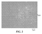
- FIG. 2 is a field emission scanning electron microscopy image of an exemplary embodiment of a conductive coating of the present disclosure.
- a conductive ink of the present disclosure includes a conductive polymer solution that can have a conductive polymer dissolved in an aqueous-based media, and a mixture of carbon nanotubes and graphene oxide sheets dispersed in the conductive polymer solution.
- the mixture of carbon nanotubes and graphene oxide sheets can serve as a hybrid nanofiller having useful properties for formulating conductive inks and forming conductive coatings of the present disclosure.
- aqueous-based media refers to liquid media for the conductive polymer solution that includes water at a level of at least 10 weight percent, at least 20 weight percent, at least 30 weight percent, at least 40 weight percent, at least 50 weight percent, at least 55 weight percent, at least 60 weight percent, at least 65 weight percent, at least 70 weight percent, at least 75 weight percent, at least 80 weight percent, at least 85 weight percent, at least 90 weight percent, or even at a level of at least 95 weight percent, relative to an overall weight of the aqueous-based media.
- the aqueous-based media can optionally include a suitable water-miscible organic solvent.
- suitable water-miscible organic solvents can include polar organic solvents having a boiling point of up to 150° C. at 1 atmosphere.
- the water-miscible organic solvent has a dipole moment of at least 1.4 Debye.
- examples of suitable water-miscible organic solvents can include one or more of alcohols, aldehyhdes, carboxylic acids, ethers, ketones, nitriles, or mixtures thereof.
- suitable water-miscible organic solvents can include one or more of acetaldehyde, acetic acid, acetone, dimethoxyethane, formic acid, methanol, ethanol, 1-propanol, 2-propanol, acetonitrile, 1,4-dioxane, tetrahydrofuran, or mixtures thereof.
- the water-miscible organic solvent if included, can be present in the aqueous-based media at a level of up to 50 weight percent, up to 40 weigh percent, up to 30 weight percent, up to 20 weight percent, up to 10 weight percent, or even up to 5 weight percent, relative to an overall weight of the aqueous-based media. The remainder of the aqueous-based media is typically water.
- Conductive inks of the present disclosure include a conductive polymer.
- the conductive polymer can provide a level of electrical conductivity in a conductive coating that results from applying and annealing a conductive ink of the present disclosure.
- the term “conductive” as used herein refers to electrical conductivity
- the term “conductive coating” refers to a coating having a sheet resistance value of less than 10 4 ohm per square. An average sheet resistance value is typically determined for thin films using a four point probe method (see, e.g., Smits, F., “Measurement of Sheet Resistivities with the Four-Point Probe”, The Bell System Technical Journal, pp. 711-718 (1958)).
- Conductive polymers or more precisely, intrinsically conducting polymers, are organic polymers that conduct electricity. They tend to have conjugated structures with alternating single and double bonds or conjugated segments coupled with atoms (e.g. N, S), providing p-orbitals for a continuous orbital overlap.
- atoms e.g. N, S
- the conductive polymer can include one or more of polythiophenes (e.g., poly(3,4-ethylenedioxythiophene)), polyanilines, polyacetylenes, polypyrroles, polycarbazoles, polyindoles, polyazepines, polyfluorenes, polyphenylenes, polyphenylene vinylenes (e.g., poly(p-phenylene vinylene)), polyphenylene sulfides (e.g., poly(p-phenylene sulfide)), polypyrenes, polyazulenes, and polynaphthalenes, or mixtures thereof.
- polythiophenes e.g., poly(3,4-ethylenedioxythiophene)
- polyanilines e.g., poly(3,4-ethylenedioxythiophene)
- polyanilines e.g., poly(3,4-ethylenedioxythiophene)
- polyanilines e.g
- a particularly useful conductive polymer is poly(3,4-ethylenedioxythiophene), and more preferably poly(3,4-ethylenedioxythiophene) doped with polystyrene sulfonate (“PEDOT:PSS”).
- PEDOT:PSS can have excellent stability to air or to heat, good transparency properties, and is lighter than conventional ITO.
- the conductive polymer can be present in the conductive polymer solution at a concentration of at least 0.05 weight percent, at least 0.1 weight percent, or even at least 0.5 weight percent relative to an overall weight of the conductive polymer solution. In some embodiments, the conductive polymer is present in the conductive polymer solution at a concentration of up to 10 weight percent, up to 5 weight percent, or even up to 2 weight percent relative to an overall weight of the conductive polymer solution.
- the conductive polymer is present in the conductive polymer solution at a concentration in a range from 0.05 weight percent to 10 weight percent, from 0.1 weight percent to 5 weight percent, from 0.5 weight percent to 5 weight percent, or even from 0.5 weight percent to 2 weight percent, relative to an overall weight of the conductive polymer solution.
- CNTs carbon nanotubes
- a conductive ink of the present disclosure includes CNTs.
- CNTs can include tubular molecules similar to graphite and having an average external diameter in a range from about 1 nanometer up to 100 nanometers and an average length in a range from 0.5 micrometers up to 100 micrometers or more.
- CNTs can have a variety of forms including, for example: single walled carbon nanotubes (“SWCNTs”), being a single sheet of one atom thick carbon atoms in a tubular shape and having a diameter as low as about 1 nanometer; double walled carbon nanotubes (“DWCNTs”), being two sheets of one atom thick sheets of carbon atoms in a tubular form and having a diameter as low as about 2 nanometers to about 4 nanometers; and multi walled carbon nanotubes (“MWCNTs”) having an appearance of concentric cylinders of one atom thick sheets of carbon atoms in a tubular form and having a diameter in a range from about 4 nanometers to about 100 nanometers.
- SWCNTs single walled carbon nanotubes
- DWCNTs double walled carbon nanotubes
- MWCNTs multi walled carbon nanotubes
- the CNTs are “pristine”, denoting CNTs that have not undergone any surface modification treatment subsequent to synthesis and/or purification, be it chemical or otherwise.
- the CNTs used in the present disclosure can be obtained commercially or prepared by methods known to those having skill in the art.
- SWCNTs can be prepared by various methods including, for example, inducing an arc-discharge through a carbon cathode and a carbon anode in an inert atmosphere (see, e.g., U.S. Published Patent Application No. 2011/0262341, Samaranayake et al.).
- the DWCNTs may be obtained by any suitable means, including, for example, contacting methane with a suitable iron on magnesia catalyst (see, e.g., U.S. Published Patent Application No. 2011/0127472, Sato et al.).
- the MWCNTs can be obtained by vapor deposition in the presence of a supported catalyst (see, e.g., U.S. Published Patent Application No. 2004/0234445, Sup et al.). Such MWCNTs can have a diameter ranging between 10 nm and 50 nm and a length that can attain 70 micrometers.
- the SWCNTs, DWCNTs, and MWCNTs can be purified by washing with acid solution (e.g., sulfuric acid, hydrochloric acid) so as to rid them of residual inorganic and metal impurities.
- acid solution e.g., sulfuric acid, hydrochloric acid
- CNTs can be obtained from commercial suppliers.
- MWCNTs having a nominal outer diameter of 8-15 nm and a nominal length of 10-30 micrometers are commercially available under the trade designation “MWCNTS SKU-030102” from Cheap Tubes, Inc. (Brattleboro, Vt.).
- aqueous-based conductive inks that include CNTs and conductive polymers, in order to obtain conductive coatings having enhanced electrical conductivity.
- efforts to formulate aqueous-based conductive inks that include CNTs are typically fraught with difficulty due to aggregation and/or precipitation of the CNTs. This aggregation and/or precipitation can be detrimental to formation of useful conductive coatings.
- a prerequisite for the good electrical conductivity of coatings that include CNTs is a fine dispersion of the CNTs in the coating. It is thought that when CNTs become increasingly associated with each other, the CNTs provide less conductivity enhancement than when the CNTs are finely dispersed.
- the CNTs can be present in the conductive ink in an amount sufficient to result in at least about 0.001 weight percent of CNTs in a conductive coating of the present disclosure. However, it is also typically desirable to provide the CNTs in the conductive ink in a suitable ratio with other components (and in particular with the graphene oxide material) to obtain a fine dispersion of CNTs in the conductive ink and in the resulting conductive coating.
- CNTs can be present in the conductive ink in an amount that is sufficient to result (i.e., after applying and annealing the conductive ink on a substrate) in a conductive coating having CNTs present in a range from 0.05 weight percent to 30 weight percent, from 0.1 weight percent to 20 weight percent, from 0.2 weight percent to 10 weight percent, or even from 0.4 weight percent to 5 weight percent, relative to an overall weight of the conductive coating.
- a conductive ink of the present disclosure includes graphene oxide (GO).
- Graphene oxide typically includes planar graphene oxide sheets (“GO sheets”) having carbon atoms arranged in a layered structure similar to graphite and having an interlayer spacing approximately two times larger than the interlayer spacing found in graphite.
- the x- and y-dimensions can typically be up to about 5 micrometers (or even up to 100 micrometers), while the average z-dimension (i.e., “thickness”) is typically less than 5 nanometers (e.g., about 0.7 to 2 nanometers) for an individual GO sheet.
- GO sheets can overlap, can stack (e.g., a few layers of graphene oxide sheets can exist stacked to a thickness of up to about 10 nanometers, or more), can fold, and, importantly, can associate with other forms of carbon, including carbon nanotubes.
- GO sheets being an oxidized form of graphene, typically have oxidized functionality, including, for example, carboxyl groups (—COOH), hydroxyl groups (—OH, including phenolic —OH groups), carbonyl groups (—C( ⁇ O)), and epoxy groups (bridging oxygen atoms) displayed around edges and on major surfaces of the GO sheets.
- oxidized functionality tends to increase the polarity (and hydrophilicity) of the GO sheets.
- GO sheets can be prepared by exposing graphite powder to strong oxidizing conditions (including exposure to oxidizing agents such as sulfuric acid, nitric acid, potassium permanganate, potassium persulfate, hydrogen peroxide, phosphorus pentoxide, or combinations thereof), using variations of the Hummers method (e.g., see Hummers et al. “Preparation of Graphite Oxide”, J. Am. Chem. Soc., 80, p. 1339 (1958); U.S. Pat. No. 2,798,878 (Hummers); and McAllister et al., “Single Sheet Functionalized Graphene by Oxidation and Thermal Expansion of Graphite”, Chem. Mater., 19, pp. 4396-4404 (2007)), although other oxidation methods know to those having skill in the art can also be used.
- oxidizing agents such as sulfuric acid, nitric acid, potassium permanganate, potassium persulfate, hydrogen peroxide, phosphorus
- Graphene oxide sheets can be made via chemical exfoliation of graphite in aqueous solution, by first introducing oxidized functionality on the carbon layers of graphite, followed by mild ultrasonication in water to exfoliate sheets of graphene oxide. It is thought that inter-lamellar coupling between the oxidized graphite layers becomes weakened by treatment with acids and/or hydrogen bonding with water, leading to the exfoliation of GO sheets (see, e.g., Zhang et al., “Size-Controlled Synthesis of Graphene Oxide Sheets on a Large Scale Using Chemical Exfoliation”, Carbon, 47, pp.
- the GO sheets can be present at a concentration of at least about 0.001 weight percent, at least 0.005 weight percent, at least 0.01 weight percent, or even at least 0.02 weight percent relative to a total weight of the conductive polymer solution. In some embodiments, the GO sheets are present in the conductive ink at a concentration of up to 0.5 weight percent, up to 0.2 weight percent, or even up to 0.1 weight percent relative to a total weight of the conductive polymer solution.
- the GO sheets are present in the conductive ink at a concentration in a range from 0.005 weight percent to 0.5 weight percent, or from 0.01 weight percent to 0.2 weight percent, or even from 0.02 weight percent to 0.1 weight percent, relative to a total weight of the conductive polymer solution.
- GO sheets can be considered to be amphiphilic, having a combination of hydrophobic domains and hydrophilic domains.
- Embodiments of conductive inks of the present disclosure take advantage of the amphiphilic properties of GO sheets to associate with both CNT and aqueous-based media, in order to enhance the dispersion of CNTs. Without being bound by theory, it is thought that the association of GO sheets with each other and with CNTs occurs at least in part through pi-stacking interactions of their respective hydrophobic domains.
- a mixture of CNTs and GO sheets is provided.
- the CNTs and GO sheets can form carbon nanotube: graphene oxide (“CNT:GO”) complexes, or hybrids, which can aid the dispersion of CNTs in aqueous-based media.
- CNT:GO carbon nanotube: graphene oxide
- a weight ratio of carbon nanotubes to graphene oxide sheets can be in a range from 0.25 to 2.5, or from 0.5 to 2, or from 0.5 to 1.5, or even from 1 to 1.5.
- the weight ratio of carbon nanotubes to graphene oxide sheets should be selected to be within a range that does not result in formation of precipitates of CNTs, GO sheets, or both.
- dispersed CNT:GO complexes in conductive inks of the present disclosure is thought to enhance the ability to form fine dispersions of CNTs in aqueous-based media, resulting in enhanced electrical conductivity in conductive coatings formed by applying and annealing the conductive ink on a substrate.
- a conductive ink of the present disclosure can include a “conductivity enhancer” (or “dopant”) material suitable for further enhancing the electrical conductivity of a coating resulting from application of the conductive ink to a substrate.
- the conductivity enhancer is selected to be able to be dispersed in the aqueous-based media and to further aid in keeping the CNTs from aggregating.
- the conductivity enhancer is dissolved in the aqueous-based media.
- the conductivity enhancer has a boiling point of at least 150° C. at a pressure of 1 atmosphere.
- suitable conductivity enhancers can include one or more of sulfoxides, alkylene glycols, dialkylene glycols, polyalkylene glycols, polyols, phenols, or mixtures thereof.
- specific examples of suitable conductivity enhancers can include dimethylsulfoxide (DMSO), ethylene glycol, diethylene glycol, glycerol, sorbitol, 2-methoxyphenol, or mixtures thereof.
- a conductivity enhancer e.g., when the conductive polymer is PEDOT:PSS
- DMSO DMSO
- the addition of a conductivity enhancer may aid in increasing interfacial connections among conductive regions in the conductive polymer, and possibly allow for alignment of conductive species during a drying of the conductive ink to form the conductive coating.
- additives can optionally be provided in a range from 0.1 weight percent to about 5 weight percent relative to a total weight of the conductive ink composition.
- the other additives can include, for example, organic dispersants, surfactants, stabilizers, or mixtures thereof.
- a conductive ink of the present disclosure can be formed by dissolving a conductive polymer in an aqueous-based media to form a conductive polymer solution, and dispersing a mixture of graphene oxide sheets, and carbon nanotubes in the conductive polymer solution. Sonication can be used to disperse GO and CNT in the aqueous-based media. The sonication time (e.g., 5 minutes to 120 minutes) and power (e.g., 20 W to 150 W) can be adjusted to aid in obtaining a dispersion of the GO and CNT in the conductive polymer solution, taking care to not induce fragmentation of CNTs by extended sonication time or elevated power conditions.
- the conductive ink can be applied to a substrate by any suitable technique, for example, one or more of spray coating, dip coating, spin coating, inkjet printing, screen printing, slot die coating, doctor knife coating, curtain coating, gravure coating, knife-over-roll coating, and roll coating.
- a suitable substrate of the present disclosure can be selected from one or more of a wide range of materials, including one or more of ceramic, polymeric, metallic, or combinations thereof.
- the substrate includes a material that is flexible such as, for example, one or more of polyethylene terephthalate, polyimide, polycarbonate, biaxially-oriented polypropylene, polystyrene, polyvinyl chloride, or combinations thereof.
- the substrate can include a flexible multilayer polymeric film that includes layers of one or more of polyethylene terephthalate, polyimide, polycarbonate, biaxially-oriented polypropylene, polystyrene, polyvinyl chloride, or combinations thereof.
- Flexible glass can also be used as a substrate, either alone or in combination with layer(s) of polymer materials.
- the substrate is selected to be transparent, flexible, or both.
- the combination of conductive coating and substrate is selected to provide an article that is flexible, transparent, or both flexible and transparent.
- flexible here refers to a film of up to 125 micrometer thickness that can be wrapped around a rod having a diameter of 1 centimeter, without breaking the film.
- transparent refers to a layer or layers that permit at least 75% of at least a portion of incident electromagnetic radiation from about 400 nm to about 700 nm to pass through the layer or layers.
- optical transmittance refers to a fraction of incident electromagnetic radiation at a specified wavelength in a range from about 400 nm to about 700 nm that passes through a sample.
- the article has an optical transmittance value at 550 nm of at least 75%, at least 80%, at least 85%, or even at least 90%.
- the conductive ink is annealed on the substrate.
- the annealing can include exposing the conductive ink on the substrate to a temperature in a range from about 80° C. to about 150° C. for a suitable time period, typically driving off most or substantially all of the water and water-miscible organic solvent (if any) from the conductive coating.
- the annealing can be carried out for any suitable time period, for example, in a range from 10 minutes to 120 minutes. In embodiments of suitable annealing conditions, no visible droplets (i.e., droplets having a size greater than 1 micrometer) are observed.
- a portion of the conductivity enhancer material may also be driven off during the annealing process, although the annealing step does not typically need to include reducing the level of conductivity enhancer remaining in the conductive coating.
- Annealing can be performed by any suitable technique, for example, one or more of infrared heating, dielectric drying, convection drying, supercritical drying, vacuum drying, or combinations thereof. While the annealing process accomplishes at least some removal of the aqueous-based media, it is also possible that the annealing process results in the conformational change of conductive polymer chains in the conductive coating as it is being formed.
- the application of conductive ink to substrate and subsequent annealing can be performed on a “roll-to-roll” apparatus, where the substrate is provided as a continuous substrate film rolled up into a substrate film roll.
- the substrate film is delivered (i.e., unrolled) from the substrate film roll, transported in its longitudinal direction, and then the conductive ink is applied to the substrate film, during transportation, by any suitable method (e.g., spraying).
- the substrate film with conductive ink applied is then subjected to the annealing conditions, during transportation, to form the conductive coating on the substrate.
- the substrate film with the conductive coating thereon can then rolled up. Parameters such as line speed, conductive ink application rate, and annealing conditions can be selected by those having skill in the art, taking into account variables such as desired coating thickness and the desired duration of annealing.
- Conductive coatings of the present disclosure include a conductive polymer and a mixture of GO sheets and CNTs dispersed in the conductive polymer.
- the amount of GO sheet material in the conductive coating is at least 0.1 weight percent, at least 0.2 weight percent, at least 0.25 weight percent, at least 0.5 weight percent, or even at least 1 weight percent, relative to the total weight of the conductive coating.
- the amount of GO sheet material in the conductive coating is up to 15 weight percent, up to 10 weight percent, or even up to 5 weight percent, relative to the total weight of the conductive coating.
- the amount of GO sheet material in the conductive coating is in a range from 0.25 weight percent to 15 weight percent, from 0.5 weight percent to 10 weight percent, or even from 1 weight percent to 5 weight percent, relative to the total weight of the conductive coating.
- the amount of CNTs in the conductive coating is at least 0.05 weight percent, at least 0.1 weight percent, at least 0.2 weight percent, or even at least 0.4 weight percent, relative to the total weight of the conductive coating. In some embodiments, the amount of CNTs in the conductive coating is up to 30 weight percent, up to 20 weight percent, up to 10 weight percent, or even up to 5 weight percent, relative to the total weight of the conductive coating. In some embodiments, the amount of CNTs in the conductive coating is in a range from 0.05 weight percent to 30 weight percent, from 0.1 weight percent to 20 weight percent, from 0.2 weight percent to 10 weight percent, or even from 0.4 weight percent to 5 weight percent, relative to the total weight of the conductive coating.
- the conductive coating of the present disclosure can include a weight ratio of CNTs to GO sheets of at least 0.25, at least 0.5, at least 0.7, at least 0.9, or even at least 1. In some embodiments the conductive coating can include a weight ratio of CNTs to GO sheets of up to 2.5, up to 2, up to 1.5, up to 1.2 or even up to 1.1. In some embodiments, the conductive coating can include a weight ratio of CNTs to GO sheets in a range from 0.25 to 2.5, from 0.5 to 2, from 0.5 to 1.5, from 1 to 1.5, or even from 1 to 1.2.
- a conductive coating of the present disclosure can have an average sheet resistance value of up to 3000 ohm per square, up to 2800 ohm per square, up to 2500 ohm per square, up to 2000 ohm per square, up to 1500 ohm per square, up to 1000 ohm per square, up to 900 ohm per square, or even up to 800 ohm per square.
- the conductive coating has an average sheet resistance value in a range from 800 ohm per square to 2800 ohm per square, from 900 ohm per square to 2800 ohm per square, or even from 800 ohm per square to 1000 ohm per square.
- the conductive polymer be transparent in the conductive coating.
- the electrically conductive coating has an optical transmittance value at 550 nm of at least 75%, or at least 80%, or at least 85%, or at least 90%, or even at least 95%.
- the conductive coating can be a film having a thickness of at least 20 nanometers, at least 30 nanometers, at least 40 nanometers, at least 50 nanometers, or even at least 60 nanometers. In some embodiments, the conductive coating is a film having a thickness of up to 250 nanometers, up to 200 nanometers, up to 150 nanometers, or even up to 120 nanometers. In some embodiments, the conductive coating is a film having a thickness in a range from 20 nanometers to 250 nanometers, from 40 nanometers to 150 nanometers, or even from 60 nanometers to 120 nanometers.
- the conductive polymer be capable of forming a flexible conductive coating on a flexible substrate.
- a flexible substrate of up to even 1 cm at least 95% of the conductivity of the flexible coating can remain when the coated substrate is wrapped around a rod with a diameter that is 80 times the thickness of the substrate.
- the annealed conductive coating can include water at a level of up to 5 weight percent, up to 4 weight percent, up to 3 weight percent, up to 2 weight percent, up to 1 weight percent, up to 0.5 weight percent, or even up to 0.1 weight percent, relative to a total weight of the conductive coating. However, it is not necessary for the conductive coating to include water in an amount up to any one of these levels in order to be electrically conductive.
- the disposition of CNTs in a conductive coating of the present disclosure preferably includes “domain networks” that are an interconnection of CNTs associated with GO sheets in a small area.
- a typical domain network dimensions can be considered to be about 10 micrometers ⁇ 10 micrometers.
- the CNTs in a domain network preferably are uniformly distributed in the conductive polymer.
- Articles of the present disclosure can be prepared by applying a conductive ink of the present disclosure to at least a portion of surface of a substrate, followed by annealing the conductive ink on the surface of the substrate to form an article having a conductive coating.
- Useful articles can include, for example, electromagnetic shielding films/fabric tapes, radio-frequency identification (RFID) tags/labels, antistatic labels/films, and transparent electrodes for flexible photovoltaic cells, electrochromic devices, flexible displays, touch screens, and organic light-emitting diodes (OLEDs).
- RFID radio-frequency identification
- a conductive ink comprising:
- the conductive polymer comprises one or more of polythiophenes, polyanilines, polyacetylenes, polypyrroles, polycarbazoles, polyindoles, polyazepines, polyfluorenes, polyphenylenes, polyphenylene vinylenes, polyphenylene sulfides, polypyrenes, polyazulenes, and polynaphthalenes, or mixtures thereof.
- aqueous-based media comprises a water-miscible organic solvent, wherein the water-miscible organic solvent has a boiling point of up to 150° C. at a pressure of 1 atmosphere.
- a conductive coating comprising:
- a method of providing a conductive coating on a substrate comprising:
- any one of embodiments 17 to 21, wherein the applying comprises one or more of spray coating, dip coating, spin coating, inkjet printing, screen printing, slot die coating, doctor knife coating, curtain coating, gravure coating, knife-over-roll coating, and roll coating.
- annealing comprises one or more of infrared heating, dielectric drying, convection drying, supercritical drying, vacuum drying, or combinations thereof.
- the substrate is a continuous substrate film rolled up into a substrate film roll, wherein the substrate film is delivered from the substrate film roll, transported in its longitudinal direction, and subjected to the applying and annealing steps during transportation, and the substrate film with the conductive coating thereon is rolled up.
- An article comprising a substrate having a surface, wherein the surface is at least partially coated with a conductive coating according to embodiment 11.
- the substrate comprises a material that is one or more of ceramic, polymeric, metallic, or combinations thereof.
- the substrate comprises one or more of polyethylene terephthalate, polyimide, polycarbonate, biaxially-oriented polypropylene, polystyrene, polyvinyl chloride, or combinations thereof.
- Graphite Natural graphite powder ⁇ 100 micrometer, Fluka, purum powder grade, obtained from Sigma Aldrich Chemical Company, St. Louis, MO MWCNT Multiwall carbon nanotube material having a nominal outer diameter of 8-15 nm and a nominal length of 10-30 micrometer, obtained from Cheap Tubes Inc., Brattleboro, VT, under the trade designation: “MWCNTS SKU-030102” H 2 SO 4 Sulfuric acid, 97%, ACS reagent grade, obtained from Sigma Aldrich Chemical Company K 2 S 2 O 8 Potassium persulfate, >99%, ACS reagent grade, obtained from Sigma Aldrich Chemical Company P 2 O 5 Phosphorus pentoxide, >98%, ACS reagent grade, obtained from Sigma Aldrich Chemical Company KMnO 4 Potassium permanganate, obtained from Sigma Aldrich Chemical Company PEDOT:PSS Poly(3,4-ethylenedioxythiophene) doped with poly(4- styrenesulfonate), CLEVI
- GO sheets were synthesized using a modified Hummers method from natural graphite powder, as described in the following details. Firstly, graphite powder (3 grams) was put into an 80° C. solution consisting of concentrated H 2 SO 4 (97 weight percent, 12 mL), K 2 S 2 O 8 (2.5 grams), and P 2 O 5 (2.5 grams). The mixture was kept at 80° C. for 6 hours using a hot plate. Successively, the mixture was cooled to room temperature and then diluted with 0.5 L of deionized water and left standing overnight.
- the pre-oxidized graphite was then subjected to further oxidation according to the following steps. Briefly, 1 gram of the pre-oxidized graphite and 0.5 gram of sodium nitrate were placed in a flask. Concentrated H 2 SO 4 (97 weight percent, 25 mL) was added with stirring in an ice-water bath, and 3 g of KMnO 4 were slowly added over about 1 hour.
- a 0.2 micrometer nylon filter obtained from Waterman International Ltd., Maidstone, England, under the trade designation “WATERMAN”
- GO sheet material prepared as described immediately above was dispersed in water (0.2 mg/mL) by ultrasonication in an ultrasound device (obtained from QSonica, LLC., Newton, Conn., under the trade designation “SONICATOR 3000”) for 30 minutes at a power of 30 W, to generate a GO colloidal suspension.
- An ultrasound device obtained from QSonica, LLC., Newton, Conn., under the trade designation “SONICATOR 3000”
- a sample of MWCNT was charged into the obtained GO colloidal suspension (proportion of MWCNT to GO was 1:2; the MWCNT sample as obtained was initially in the form of agglomerates), and the mixture was further ultrasonicated for 1 hour at 30 W to give a suspension of the GO-MWCNT complexes.
- a control suspension of MWCNTs was also prepared in the same way except that the GO sheet material was not included.
- the suspension of the GO-MWCNT complex and the control suspension of MWCNT were each examined by atomic force microscopic (“AFM”) measurements with various modes using an AFM instrument (obtained from Asylum Research, Goleta, Calif., under the trade designation “MODEL MFP-3D-BIO”).
- AFM atomic force microscopic
- the samples for AFM were prepared by dropping aliquots of the suspensions onto fresh silicon wafers, followed by drying them under ambient conditions.
- the AFM digital images in FIGS. 1A and 1B have x and y dimensions in units of micrometers, and a z dimension in units of nanometers, as indicated in the shaded bar to the right of each digital image.
- FIG. 1B is an AFM digital image of the GO-MWCNT complexes that were observed in the dried AFM samples to be spaghetti-like MWCNTs 115 randomly associated with GO sheets 120 , as shown in the AFM image in FIG. 1B , with no observations of serious MWCNT aggregation.
- a 3 mL sample of GO sheet material dispersed in water (1.0 mg/mL; sonication was used to disperse the GO sheet material in water) was dispersed in 12 mL PEDOT:PSS solution (1.3 weight percent in water) to achieve a fixed concentration of the GO sheet material (0.2 milligram GO sheet material per mL of dispersion in a PEDOT:PSS solution).
- a selected amount of MWCNT was added to obtain the range of MWCNT to GO weight ratios for Examples 1 to 6 as shown in Table 1, below.
- Each of these mixtures was ultrasonicated for 1 hour at a power of 30 W to generate the GO-MWCNT/PEDOT:PSS dispersions.
- dimethylsulfoxide (5% volume ratio) was incorporated into each of the GO-MWCNT/PEDOT:PSS dispersions to achieve the conductive inks of Examples 1 to 6.
- These inks were sprayed onto the pretreated glass substrates (pretreated by soaking and ultrasonication in acetone, 2-propanol, and deionized water for 30 minutes each) using an airbrush, and the resulting conductive coatings were annealed at 100° C. for 20 minutes. Parameters such as the pressure of compressed nitrogen gas (80 p.s.i.), spraying angle (45°) and distance (30 cm), and ink volume (2 mL) were kept consistent during all spraying processes.
- Thickness of the dry coatings was in a range of 60 to 120 nm.
- the resulting conductive coatings were designated as Examples 1-6 samples according to their initial proportion of MWCNT to GO during the formulation of corresponding inks.
- Control samples of PEDOT:PSS, MWCNT/PEDOT:PSS, and GO/PEDOT:PSS composite coatings (denoted as Comparative Example A, Comparative Example B and Comparative Example C, respectively) were also prepared for comparison, using essentially the same protocol. Table 1 summarizes the samples and measured properties for Examples 1 to 6 and Comparative Examples A to C.
- optical transparency of the conductive coatings deposited on glass substrates was characterized using a UV-Vis spectrometer (obtained from Varian Australia, Mulgrave, VIC, Australia, under the trade designation “CARY 50 BIO SPECTROMETER”) at normal incidence.
- Optical transmittance values at 550 nm for Examples 1 to 6 are summarized in Table 1. Since the GO concentration was constant across Examples 1 to 6 all samples, the MWCNT concentration appeared to have a direct effect on optical transmittance. It was also visually observed that the coatings having higher MWCNT concentrations appeared less transparent.
- Example 5 had a higher weight ratio of MWCNTs:GO sheets (i.e., 2:1), and while dispersed MWCNTs were observed via SEM (not shown), small bundles were also observed in the polymer matrix.
- the conductive coating of Example 5 revealed higher resistivity than in Example 3. Further increasing the proportion of MWCNTs to GO sheets further diminished the conductivity of the PEDOT:PSS coating, as reflected by increased resistivity observed for Example 6.
- Comparative Example B The sheet resistance of Comparative Example B was about 2700 ohms per square, which was lower than that of Comparative Example A; possibly the presence of the MWCNTs improved the conductivity of PEDOT:PSS due to an inherent conductivity of the MWCNTs. However, the sheet resistance of Comparative Example B was nearly 3 times higher than that of Example 3, even though they had equal MWCNT concentration (i.e., 0.2 mg/mL), suggesting a strong dispersant role of GO sheets in Example 3.
- Example 3 and Comparative Example B were examined via SEM. Finely dispersed MWCNTs were observed in Example 3 samples (e.g., 201 in FIG. 2 ), while a large MWCNT bundle was visible in Comparative Example B sample (not shown) suggesting that perhaps only a dispersed portion of MWCNTs in Comparative Example B sample contributed to the observed conductivity. MWCNT bundles were also observed in Example 6 samples, where the MWCNT concentration in the conductive ink was calculated to be 0.5 weight percent.
- Comparative Example C sample had a sheet resistance of 4000 ⁇ 225 ohms per square, which was very close to that of pure PEDOT:PSS coating of Comparative Example A (4100 ⁇ 300 ohms per square), suggesting that GO sheets in the absence of MWCNT did not provide significant additional conductivity beyond that of PEDOT:PSS alone.
Landscapes
- Chemical & Material Sciences (AREA)
- Engineering & Computer Science (AREA)
- Organic Chemistry (AREA)
- Life Sciences & Earth Sciences (AREA)
- Materials Engineering (AREA)
- Wood Science & Technology (AREA)
- Physics & Mathematics (AREA)
- Spectroscopy & Molecular Physics (AREA)
- Chemical Kinetics & Catalysis (AREA)
- Dispersion Chemistry (AREA)
- General Chemical & Material Sciences (AREA)
- Nanotechnology (AREA)
- Inks, Pencil-Leads, Or Crayons (AREA)
- Conductive Materials (AREA)
- Compositions Of Macromolecular Compounds (AREA)
- Paints Or Removers (AREA)
- Manufacturing Of Electric Cables (AREA)
- Thermal Sciences (AREA)
- Manufacturing & Machinery (AREA)
Priority Applications (1)
| Application Number | Priority Date | Filing Date | Title |
|---|---|---|---|
| US14/437,536 US9803097B2 (en) | 2012-10-29 | 2013-10-21 | Conductive inks and conductive polymeric coatings |
Applications Claiming Priority (3)
| Application Number | Priority Date | Filing Date | Title |
|---|---|---|---|
| US201261719560P | 2012-10-29 | 2012-10-29 | |
| US14/437,536 US9803097B2 (en) | 2012-10-29 | 2013-10-21 | Conductive inks and conductive polymeric coatings |
| PCT/US2013/065919 WO2014070500A1 (en) | 2012-10-29 | 2013-10-21 | Conductive inks and conductive polymeric coatings |
Publications (2)
| Publication Number | Publication Date |
|---|---|
| US20150275016A1 US20150275016A1 (en) | 2015-10-01 |
| US9803097B2 true US9803097B2 (en) | 2017-10-31 |
Family
ID=50627946
Family Applications (1)
| Application Number | Title | Priority Date | Filing Date |
|---|---|---|---|
| US14/437,536 Expired - Fee Related US9803097B2 (en) | 2012-10-29 | 2013-10-21 | Conductive inks and conductive polymeric coatings |
Country Status (5)
| Country | Link |
|---|---|
| US (1) | US9803097B2 (enExample) |
| EP (1) | EP2912123B1 (enExample) |
| JP (1) | JP6192732B2 (enExample) |
| CN (1) | CN104797666A (enExample) |
| WO (1) | WO2014070500A1 (enExample) |
Cited By (1)
| Publication number | Priority date | Publication date | Assignee | Title |
|---|---|---|---|---|
| US12376443B2 (en) | 2022-09-30 | 2025-07-29 | Energy Materials Corporation | Photovoltaic structures having a composite conductor |
Families Citing this family (35)
| Publication number | Priority date | Publication date | Assignee | Title |
|---|---|---|---|---|
| TWI525643B (zh) * | 2012-11-09 | 2016-03-11 | 財團法人工業技術研究院 | 導電油墨組成物及透明導電薄膜 |
| CN104059432B (zh) * | 2013-03-20 | 2016-01-06 | 北京阿格蕾雅科技发展有限公司 | 透明碳纳米管高分子复合导电墨水及其制备方法 |
| DE102013225904B8 (de) * | 2013-12-13 | 2016-09-29 | Humboldt-Universität Zu Berlin | Beschichtungsmittel zum Herstellen einer elektrisch leitfähigen Schicht und Verfahren zu dessen Herstellung |
| CN105244443B (zh) * | 2014-07-10 | 2017-10-17 | 华为技术有限公司 | 一种透明电极及其制备方法和有机太阳能电池 |
| TWI533767B (zh) | 2014-07-14 | 2016-05-11 | 安炬科技股份有限公司 | 石墨烯印刷線路結構 |
| CN105321592B (zh) * | 2014-08-01 | 2017-03-22 | 广东阿格蕾雅光电材料有限公司 | 碳纳米管‑高分子层状复合透明柔性电极及其制备方法 |
| CN104212241B (zh) * | 2014-09-01 | 2017-01-18 | 江苏格美高科技发展有限公司 | 一种高导热的聚合物导电油墨及其生产工艺 |
| CN104212242B (zh) * | 2014-09-02 | 2016-08-24 | 江苏格美高科技发展有限公司 | 一种喷墨用石墨烯与碳纳米管导电油墨的制备方法 |
| US20160137875A1 (en) * | 2014-11-13 | 2016-05-19 | Rice University | Conductive polymer coating composition |
| WO2016090087A1 (en) * | 2014-12-05 | 2016-06-09 | Rhodia Operations | Electrically conductive polymer films and complexes containing a conductivity enhancing agent, and electronic devices containing such films and complexes |
| GB201503398D0 (en) * | 2015-02-27 | 2015-04-15 | Perpetuus Res & Dev Ltd | A particle dispersion |
| CN105038411B (zh) * | 2015-07-14 | 2018-04-27 | 浙江中科立德新材料有限公司 | 一种导电油墨及其制备方法和使用方法 |
| GB2545172B (en) * | 2015-12-03 | 2021-05-12 | Fgv Cambridge Nanosystems Ltd | Carbon nanotube/graphene composites |
| CN105679394B (zh) * | 2016-01-27 | 2017-07-14 | 广州中国科学院先进技术研究所 | Uv导电浆及由其印刷出银纳米线柔性透明导电膜的方法 |
| WO2017149499A1 (en) * | 2016-03-04 | 2017-09-08 | King Abdullah University Of Science And Technology | 3d noncontact humidity sensing technologies and methods of use thereof |
| US20190366722A1 (en) * | 2017-01-25 | 2019-12-05 | University Of South Carolina | Printable Graphene Oxide Coatings and Membranes |
| CN109277228A (zh) * | 2017-07-21 | 2019-01-29 | 株式会社科威-艾乐 | 基板处理装置 |
| PL237958B1 (pl) * | 2018-01-03 | 2021-06-14 | Politechnika Slaska Im Wincent | Kompozycja stanowiąca pastę lub atrament do druku powłok przewodzących prąd elektryczny |
| US20190235339A1 (en) * | 2018-01-29 | 2019-08-01 | Polyceed Inc. | Electrochromic device structures with conductive nanoparticles |
| CN110157244A (zh) * | 2018-02-05 | 2019-08-23 | 北京欧美中科学技术研究院 | 一种新型环保导电油墨用石墨烯添加剂的制备方法 |
| CN108346493B (zh) * | 2018-02-27 | 2019-08-02 | 合肥微晶材料科技有限公司 | 一种通过改变等离子体共振强度降低纳米银线透明导电膜黄度的方法 |
| CN110157245A (zh) * | 2018-03-01 | 2019-08-23 | 济南开发区星火科学技术研究院 | 一种新型环保导电油墨用石墨烯添加剂的制备方法 |
| CN108641486A (zh) * | 2018-04-13 | 2018-10-12 | 重庆市中光电显示技术有限公司 | 电容式触摸屏用碳导电油墨及其制备方法与应用 |
| JP7190694B2 (ja) * | 2018-12-06 | 2022-12-16 | 株式会社マルアイ | Rfidの導電性パターンの製造方法 |
| JP7550166B2 (ja) | 2019-04-03 | 2024-09-12 | スリーエム イノベイティブ プロパティズ カンパニー | 光学フィルム及びガラスラミネート |
| FI129918B (en) * | 2019-05-02 | 2022-10-31 | Turun Yliopisto | A method of making a film |
| AU2020308851B2 (en) * | 2019-06-25 | 2026-03-26 | Kansas State University Research Foundation | Nano-inks of carbon nanomaterials for printing and coating |
| CN110189621A (zh) * | 2019-06-27 | 2019-08-30 | 上海碳源汇谷新材料科技有限公司 | 一种基于石墨烯的防伪标签 |
| CN110369242A (zh) * | 2019-07-26 | 2019-10-25 | 马鞍山钢铁股份有限公司 | 一种防氧化烧损基材的制造工艺及防氧化烧损钢坯制品 |
| CN112509729B (zh) * | 2019-09-16 | 2023-01-24 | 天津工业大学 | 一种柔性透明导电薄膜及其制备方法 |
| CN112263255B (zh) * | 2020-09-28 | 2026-03-24 | 北京师范大学 | 一种基于导电聚合物转移的石墨烯皮肤电极及其制备方法 |
| US20250136834A1 (en) * | 2022-01-28 | 2025-05-01 | Cabot Corporation | Conductive Ink with Carbon Nanostructures |
| CN114773534B (zh) * | 2022-03-24 | 2023-11-07 | 广东邦固化学科技有限公司 | 一种导电pua复合乳液及其制备方法 |
| CH719600B1 (fr) * | 2022-04-12 | 2024-09-30 | Graphenaton Tech Sa | Procédé de fabrication d'une structure électronique multicouches flexible. |
| WO2024132527A1 (en) * | 2022-12-21 | 2024-06-27 | Heliosonic Gmbh | Printing ink containing particles of non-amorphous carbon allotropes |
Citations (23)
| Publication number | Priority date | Publication date | Assignee | Title |
|---|---|---|---|---|
| US2798878A (en) | 1954-07-19 | 1957-07-09 | Nat Lead Co | Preparation of graphitic acid |
| US20040234445A1 (en) | 2001-06-28 | 2004-11-25 | Serp Philippe Gilles | Method for the selective production of ordered carbon nanotubes in a fluidised bed |
| JP2007534780A (ja) | 2003-10-21 | 2007-11-29 | イー・アイ・デュポン・ドウ・ヌムール・アンド・カンパニー | ポリアニリンおよびカーボンナノチューブを含有する絶縁ポリマー |
| US20070284557A1 (en) * | 2006-06-13 | 2007-12-13 | Unidym, Inc. | Graphene film as transparent and electrically conducting material |
| WO2008051719A1 (en) | 2006-10-24 | 2008-05-02 | 3M Innovative Properties Company | Conductive ink formulations |
| US20080302561A1 (en) | 2005-10-14 | 2008-12-11 | The Trustees Of Princeton Universitty | Conductive ink containing thermally exfoliated graphite oxide and method of making a conductive circuit using the same |
| US20090226684A1 (en) | 2008-02-13 | 2009-09-10 | Bayer Materialscience Ag | Printable Composition Containing Carbon Nanotubes, Processes for Their Preparation and Electrically Conductive Coating Prepared Therefrom |
| US20100000441A1 (en) | 2008-07-01 | 2010-01-07 | Jang Bor Z | Nano graphene platelet-based conductive inks |
| WO2010112680A1 (fr) | 2009-03-31 | 2010-10-07 | Hutchinson | Films ou revetements transparents conducteurs |
| US20110040007A1 (en) | 2009-08-17 | 2011-02-17 | Laird Technologies, Inc. | Highly thermally-conductive moldable thermoplastic composites and compositions |
| US20110127472A1 (en) | 2007-02-20 | 2011-06-02 | Kenichi Sato | Carbon nanotube assembly and electrically conductive film |
| US20110262341A1 (en) | 2010-04-25 | 2011-10-27 | Sri Lanka Institute of Nanotechnology (Pvt) Ltd. | Process for preparation of carbon nanotubes from vein graphite |
| US20110319554A1 (en) | 2008-11-25 | 2011-12-29 | The Board Of Trustees Of The University Of Alabama | Exfoliation of graphite using ionic liquids |
| US20120015098A1 (en) | 2010-07-14 | 2012-01-19 | Qian Cheng | Carbon nanotube based transparent conductive films and methods for preparing and patterning the same |
| JP2012502187A (ja) | 2008-09-12 | 2012-01-26 | エルジー・ケム・リミテッド | 金属ナノベルト、その製造方法、それを含む導電性インク組成物および伝導性フィルム |
| US20120111599A1 (en) | 2010-11-05 | 2012-05-10 | United States Of America As Represented By The Administrator Of The National Aeronautics And Spac | Inkjet Printing of Conductive Carbon Nanotubes, Inherently Conductive Polymers, and Metal Particle Inks |
| US20120128570A1 (en) | 2008-10-11 | 2012-05-24 | Vorbeck Materials Corp. | Process for the preparation of graphite oxide and graphene sheets |
| US20120168682A1 (en) | 2010-12-30 | 2012-07-05 | Samsung Electro-Mechanics Co., Ltd. | Pedot/pss composition and pedot/pss film using the same |
| JP2013035966A (ja) | 2011-08-09 | 2013-02-21 | Mitsubishi Gas Chemical Co Inc | 導電性塗料 |
| JP2013122884A (ja) | 2011-12-12 | 2013-06-20 | Toshiba Corp | 透明導電材料、分散液、透明導電膜、及びそれらの製造方法 |
| US20140320959A1 (en) * | 2013-04-29 | 2014-10-30 | Lg Display Co., Ltd. | Antistatic film, method for manufacturing the same, and display device including the same |
| US20150024122A1 (en) * | 2013-07-16 | 2015-01-22 | Enerage Inc. | Graphene ink and method for manufacturing graphene pattern using the same |
| US20150114952A1 (en) * | 2013-10-24 | 2015-04-30 | National Tsing Hua University | Flexible transparent film heater |
-
2013
- 2013-10-21 US US14/437,536 patent/US9803097B2/en not_active Expired - Fee Related
- 2013-10-21 WO PCT/US2013/065919 patent/WO2014070500A1/en not_active Ceased
- 2013-10-21 CN CN201380056803.2A patent/CN104797666A/zh active Pending
- 2013-10-21 EP EP13850519.3A patent/EP2912123B1/en not_active Not-in-force
- 2013-10-21 JP JP2015539688A patent/JP6192732B2/ja not_active Expired - Fee Related
Patent Citations (25)
| Publication number | Priority date | Publication date | Assignee | Title |
|---|---|---|---|---|
| US2798878A (en) | 1954-07-19 | 1957-07-09 | Nat Lead Co | Preparation of graphitic acid |
| US20040234445A1 (en) | 2001-06-28 | 2004-11-25 | Serp Philippe Gilles | Method for the selective production of ordered carbon nanotubes in a fluidised bed |
| JP2007534780A (ja) | 2003-10-21 | 2007-11-29 | イー・アイ・デュポン・ドウ・ヌムール・アンド・カンパニー | ポリアニリンおよびカーボンナノチューブを含有する絶縁ポリマー |
| US8048214B2 (en) | 2005-10-14 | 2011-11-01 | The Trustees Of Princeton University | Conductive ink containing thermally exfoliated graphite oxide and method a conductive circuit using the same |
| US20080302561A1 (en) | 2005-10-14 | 2008-12-11 | The Trustees Of Princeton Universitty | Conductive ink containing thermally exfoliated graphite oxide and method of making a conductive circuit using the same |
| US20070284557A1 (en) * | 2006-06-13 | 2007-12-13 | Unidym, Inc. | Graphene film as transparent and electrically conducting material |
| US20090017211A1 (en) | 2006-06-13 | 2009-01-15 | Unidym, Inc. | Graphene film as transparent and electrically conducting material |
| WO2008051719A1 (en) | 2006-10-24 | 2008-05-02 | 3M Innovative Properties Company | Conductive ink formulations |
| US20110127472A1 (en) | 2007-02-20 | 2011-06-02 | Kenichi Sato | Carbon nanotube assembly and electrically conductive film |
| US20090226684A1 (en) | 2008-02-13 | 2009-09-10 | Bayer Materialscience Ag | Printable Composition Containing Carbon Nanotubes, Processes for Their Preparation and Electrically Conductive Coating Prepared Therefrom |
| US20100000441A1 (en) | 2008-07-01 | 2010-01-07 | Jang Bor Z | Nano graphene platelet-based conductive inks |
| JP2012502187A (ja) | 2008-09-12 | 2012-01-26 | エルジー・ケム・リミテッド | 金属ナノベルト、その製造方法、それを含む導電性インク組成物および伝導性フィルム |
| US20120128570A1 (en) | 2008-10-11 | 2012-05-24 | Vorbeck Materials Corp. | Process for the preparation of graphite oxide and graphene sheets |
| US20110319554A1 (en) | 2008-11-25 | 2011-12-29 | The Board Of Trustees Of The University Of Alabama | Exfoliation of graphite using ionic liquids |
| WO2010112680A1 (fr) | 2009-03-31 | 2010-10-07 | Hutchinson | Films ou revetements transparents conducteurs |
| US20110040007A1 (en) | 2009-08-17 | 2011-02-17 | Laird Technologies, Inc. | Highly thermally-conductive moldable thermoplastic composites and compositions |
| US20110262341A1 (en) | 2010-04-25 | 2011-10-27 | Sri Lanka Institute of Nanotechnology (Pvt) Ltd. | Process for preparation of carbon nanotubes from vein graphite |
| US20120015098A1 (en) | 2010-07-14 | 2012-01-19 | Qian Cheng | Carbon nanotube based transparent conductive films and methods for preparing and patterning the same |
| US20120111599A1 (en) | 2010-11-05 | 2012-05-10 | United States Of America As Represented By The Administrator Of The National Aeronautics And Spac | Inkjet Printing of Conductive Carbon Nanotubes, Inherently Conductive Polymers, and Metal Particle Inks |
| US20120168682A1 (en) | 2010-12-30 | 2012-07-05 | Samsung Electro-Mechanics Co., Ltd. | Pedot/pss composition and pedot/pss film using the same |
| JP2013035966A (ja) | 2011-08-09 | 2013-02-21 | Mitsubishi Gas Chemical Co Inc | 導電性塗料 |
| JP2013122884A (ja) | 2011-12-12 | 2013-06-20 | Toshiba Corp | 透明導電材料、分散液、透明導電膜、及びそれらの製造方法 |
| US20140320959A1 (en) * | 2013-04-29 | 2014-10-30 | Lg Display Co., Ltd. | Antistatic film, method for manufacturing the same, and display device including the same |
| US20150024122A1 (en) * | 2013-07-16 | 2015-01-22 | Enerage Inc. | Graphene ink and method for manufacturing graphene pattern using the same |
| US20150114952A1 (en) * | 2013-10-24 | 2015-04-30 | National Tsing Hua University | Flexible transparent film heater |
Non-Patent Citations (36)
| Title |
|---|
| Bhandari, "Poly(3,4-ethylenedioxythiophene)-Multiwalled Carbon Nanotube Composite Films: Structure-Directed Amplified Electrochromic Response and Improved Redox Activity", J. Phys. Chem. B, 2009, vol. 113, pp. 9416-9428. |
| Cai et al., Highly Conductive Carbon-Nanotube/Graphite-Oxide Hybrid Films, Advanced Materials, vol. 20, No. 9, May 5, 2008, pp. 1706-1709. |
| Cai, et al., Highly Conductive Carbon-Nanotube/Graphite-Oxide Hybrid Films, Advanced Materials, vol. 20, No. 9, May 5, 2008, 4 pages. |
| Dreyer, "The chemistry of graphene oxide", Chemical Society Reviews, 2010, vol. 39, pp. 228-240. |
| Extended European Search Report, EP13850519.3, dated May 25, 2016. |
| Geim, "Graphene: Status and Prospects", Science, Jun. 2009, vol. 324, pp. 1530-1534. |
| Geim, "The rise of graphene", Nature Materials, Mar. 2007, vol. 6, pp. 183-191. |
| Guo et al., Assembled graphene oxide and single-walled carbon nanotube ink for stable supercapacitors, Journal of Materials Research, Apr. 2013, vol. 28, Issue 7, pp. 918-926. |
| Hecht, "Conductivity scaling with bundle length and diameter in single walled carbon nanotube networks", Applied Physics Letters, 2006, vol. 89, pp. 133112-1-133112-3. |
| Hecht, "Solution-processed transparent electrodes", MRS Bulletin, Oct. 2011, vol. 36, pp. 749-755. |
| Hummers, "Preparation of Graphitic Oxide", J. Am. Chem. Soc., 1958, vol. 80, No. 6, pp. 1339. |
| International Search Report for PCT International Application No. PCT/US2013/065919 dated Dec. 18, 2013, 4 pages. |
| J. Yan et al. "Preparation of graphene/nanosheet/carbon nanotube/polyaniline composite as electrode material for supercapacitors," Journal of Power Sources 195 (2010) 3041-3045. * |
| Jo, "Stable Aqueous Dispersion of Reduced Graphene Nanosheets via Non-Covalent Functionalization with Conducting Polymers and Application in Transparent Electrodes", Langmuir, 2011, vol. 27, No. 5, pp. 2014-2018. |
| Kim, "Graphene Oxide Sheets at Interfaces", J. Am. Chem. Soc., 2010, vol. 132, pp. 8180-8186. |
| Kovtyukhova, "Layer-by-Layer Assembly of Ultrathin Composite Films from Micron-Sized Graphite Oxide Sheets and Polycations", Chem. Mater., 1999, vol. 11, No. 3, pp. 771-778. |
| Li, "Synergistic effect of hybrid carbon nantube-graphene oxide as a nanofiller in enhancing the mechanical properties of PVA composites", Journal of Materials Chemistry, 2011, vol. 21, pp. 10844-10851. |
| Lok, "Inkjet Printing of Multi-Walled Carbon Nanotube/Polymer Composite Thin Film for Interconnection", Journal of Nanoscience and Nanotechnology, 2010, vol. 10, No. 7, pp. 4711-4715. |
| Lu, "A flexible graphene/multiwalled carbon nanotube film as a high performance electrode material for supercapacitors", Electrochimica Acta, 2011, vol. 56, pp. 5115-5121. |
| Marcano, "Improved Synthesis of Graphene Oxide", Acsnano, Jul. 2010, vol. 4, No. 8, pp. 4806-4814. |
| McAllister, "Single Sheet Functionalized Graphene by Oxidation and Thermal Expansion of Graphite", Chem. Mater., 2007, vol. 19, pp. 4396-4404. |
| Moon, "Transparent conductive film based on carbon nanotubes and PEDOT composites", Diamond & Related Materials, 2005, vol. 14, pp. 1882-1887. |
| Novoselov, "Electric Field Effect in Atomically Thin Carbon Films", Science, 2004, vol. 306, pp. 666-669. |
| Shen, "Synthesis of Amphiphilic Graphene Nanoplatelets", Small Journal, 2009, vol. 5, No. 1, pp. 82-85. |
| Sinani, "Aqueous Dispersions of Single-wall and Multiwall Carbon Nanotubes with Designed Amphiphilic Polycations", J. Am. Chem. Soc., 2005, vol. 127, No. 10, pp. 3463-3472. |
| Sinitskii, "Chemical Approaches to Produce Graphene Oxide and Related Materials", Graphene Nanoelectronics, 2012, pp. 205-234. |
| Smits, "Measurement of Sheet Resistivities with the Four-Point Probe", The Bell System Technical Journal, May 1958, pp. 711-718. |
| Tian, "Graphene Oxides for Homogeneous Dispersion of Carbon Nanotubes" ACS Applied Materials & Interfaces, 2010, vol. 2, No. 11, pp. 3217-3222. |
| Tung, "Surfactant-Free Water-Processable Photoconductive All-Carbon Composite", J. Am. Chem. Soc., 2011, vol. 133, pp. 4940-4947. |
| Viculis, "A Chemical Route to Carbon Nanoscrolls" Science, Feb. 2003, vol. 299, p. 1361. |
| Yun, "Composite Films of Oxidized Multiwall Carbon Nanotube and Poly(3,4-ethylenedioxythiophene): Polystyrene Sulfonate (PEDOT:PSS) As a Contact Electrode for Transistor and Inverter Devices", ACS Applied Materials & Interfaces, 2012, vol. 4, pp. 982-989. |
| Yun, "Multiwall Carbon Nanotube and Poly (3,4-ethylenedioxythiophene): Polystyrene Sulfonate (PEDOT:PSS) Composite Films for Transistor and Inverter Devices", ACS Applied Materials & Interfaces, 2011, vol. 3, No. 1, pp. 43-49. |
| Zhang, "Graphene Oxide-Assisted Dispersion of Pristine Multiwalled Carbon Nanotubes in Aqueous Media", J. Phys. Chem. C., 2010, vol. 114, pp. 11435-11440. |
| Zhang, "Size-controlled synthesis of graphene oxide sheets on a large scale using chemical exfoliation", Carbon, 2009, vol. 47, pp. 3365-3380. |
| Zheng, "Transparent Conductive Films Consisting of Ultralarge Graphene Sheets Produced by Langmuir-Blodgett Assembly", Acsnano, 2011, vol. 5, No. 7, pp. 6039-6051. |
| Zheng, "Transparent Conductive Films Consisting of Ultralarge Graphene Sheets Produced by Langmuir—Blodgett Assembly", Acsnano, 2011, vol. 5, No. 7, pp. 6039-6051. |
Cited By (1)
| Publication number | Priority date | Publication date | Assignee | Title |
|---|---|---|---|---|
| US12376443B2 (en) | 2022-09-30 | 2025-07-29 | Energy Materials Corporation | Photovoltaic structures having a composite conductor |
Also Published As
| Publication number | Publication date |
|---|---|
| JP6192732B2 (ja) | 2017-09-06 |
| CN104797666A (zh) | 2015-07-22 |
| WO2014070500A1 (en) | 2014-05-08 |
| EP2912123A4 (en) | 2016-06-22 |
| EP2912123A1 (en) | 2015-09-02 |
| EP2912123B1 (en) | 2017-11-22 |
| JP2016505077A (ja) | 2016-02-18 |
| US20150275016A1 (en) | 2015-10-01 |
Similar Documents
| Publication | Publication Date | Title |
|---|---|---|
| US9803097B2 (en) | Conductive inks and conductive polymeric coatings | |
| Wang et al. | Novel biodegradable and ultra-flexible transparent conductive film for green light OLED devices | |
| Reddy et al. | Coating of multiwalled carbon nanotubes with polymer nanospheres through microemulsion polymerization | |
| Kang et al. | Direct exfoliation of graphite using a non-ionic polymer surfactant for fabrication of transparent and conductive graphene films | |
| Tung et al. | Poly (ionic liquid)-stabilized graphene sheets and their hybrid with poly (3, 4-ethylenedioxythiophene) | |
| Peter Chen et al. | Highly conductive carbon nanotube buckypapers with improved doping stability via conjugational cross-linking | |
| Qi et al. | Synthesis of graphene–conjugated polymer nanocomposites for electronic device applications | |
| Deetuam et al. | Synthesis of well dispersed graphene in conjugated poly (3, 4-ethylenedioxythiophene): polystyrene sulfonate via click chemistry | |
| US9902866B2 (en) | Methods for preparation of concentrated graphene ink compositions and related composite materials | |
| Vivekchand et al. | Electrical properties of inorganic nanowire–polymer composites | |
| US20160254070A1 (en) | Hybrid pani/carbon nano-composites for production of thin, transparent and conductive films | |
| Bkakri et al. | Degree of phase separation effects on the charge transfer properties of P3HT: Graphene nanocomposites | |
| Mo et al. | Flexible transparent conductive films combining flexographic printed silver grids with CNT coating | |
| US20100102281A1 (en) | Conductive film and method for manufacturing the same, and electronic apparatus and method for manufacturing the same | |
| Liu et al. | High conductivity and transparency of graphene-based conductive ink: Prepared from a multi-component synergistic stabilization method | |
| WO2018107795A1 (zh) | 一种球磨剥离白石墨烯的方法 | |
| ChandraKishore et al. | Facile synthesis of carbon nanotubes and their use in the fabrication of resistive switching memory devices | |
| US20140087164A1 (en) | Transparent conductive films with carbon nanotubes, inks to form the films and corresponding processes | |
| TW201134896A (en) | Large-area transparent conductive coatings including alloyed carbon nanotubes and nanowire composites, and methods of making the same | |
| JP2007527107A (ja) | 表面上に少なくとも一つの複合色素を有するチューブ状ナノ構造を少なくとも1種類備えた装置 | |
| KR20150085523A (ko) | 그래핀 소재와 전도성 중합체를 포함한 막 형성용 조성물 | |
| JP6744406B2 (ja) | n型半導体層、熱電変換層、熱電変換素子、熱電変換モジュール、及びn型半導体層形成用組成物 | |
| Wang et al. | Strong adhesion and high optoelectronic performance hybrid graphene/carbon nanotubes transparent conductive films for green-light OLED devices | |
| Park et al. | Preparation of water soluble graphene using polyethylene glycol: comparison of covalent approach and noncovalent approach | |
| Azoubel et al. | Controlling Adhesion Properties of SWCNT–PET Films Prepared by Wet Deposition |
Legal Events
| Date | Code | Title | Description |
|---|---|---|---|
| AS | Assignment |
Owner name: 3M INNOVATIVE PROPERTIES COMPANY, MINNESOTA Free format text: ASSIGNMENT OF ASSIGNORS INTEREST;ASSIGNORS:BAO, HONGQIAN;ZIN, MELVIN;JULIUS, DAVID;AND OTHERS;SIGNING DATES FROM 20150223 TO 20150408;REEL/FRAME:035466/0584 |
|
| STCF | Information on status: patent grant |
Free format text: PATENTED CASE |
|
| CC | Certificate of correction | ||
| FEPP | Fee payment procedure |
Free format text: MAINTENANCE FEE REMINDER MAILED (ORIGINAL EVENT CODE: REM.); ENTITY STATUS OF PATENT OWNER: LARGE ENTITY |
|
| LAPS | Lapse for failure to pay maintenance fees |
Free format text: PATENT EXPIRED FOR FAILURE TO PAY MAINTENANCE FEES (ORIGINAL EVENT CODE: EXP.); ENTITY STATUS OF PATENT OWNER: LARGE ENTITY |
|
| STCH | Information on status: patent discontinuation |
Free format text: PATENT EXPIRED DUE TO NONPAYMENT OF MAINTENANCE FEES UNDER 37 CFR 1.362 |
|
| FP | Lapsed due to failure to pay maintenance fee |
Effective date: 20211031 |