US9739830B2 - Test assembly - Google Patents
Test assembly Download PDFInfo
- Publication number
- US9739830B2 US9739830B2 US14/275,783 US201414275783A US9739830B2 US 9739830 B2 US9739830 B2 US 9739830B2 US 201414275783 A US201414275783 A US 201414275783A US 9739830 B2 US9739830 B2 US 9739830B2
- Authority
- US
- United States
- Prior art keywords
- circuit board
- disposed
- test
- main circuit
- pads
- Prior art date
- Legal status (The legal status is an assumption and is not a legal conclusion. Google has not performed a legal analysis and makes no representation as to the accuracy of the status listed.)
- Active, expires
Links
- 238000012360 testing method Methods 0.000 title claims abstract description 119
- 239000000523 sample Substances 0.000 claims abstract description 73
- 239000004065 semiconductor Substances 0.000 claims abstract description 13
- 239000003351 stiffener Substances 0.000 claims description 7
- 230000002950 deficient Effects 0.000 description 8
- 230000008901 benefit Effects 0.000 description 4
- 238000005476 soldering Methods 0.000 description 4
- 230000003247 decreasing effect Effects 0.000 description 1
- 239000003292 glue Substances 0.000 description 1
- 238000004519 manufacturing process Methods 0.000 description 1
- 238000012986 modification Methods 0.000 description 1
- 230000004048 modification Effects 0.000 description 1
- 239000011347 resin Substances 0.000 description 1
- 229920005989 resin Polymers 0.000 description 1
Images


Classifications
-
- G—PHYSICS
- G01—MEASURING; TESTING
- G01R—MEASURING ELECTRIC VARIABLES; MEASURING MAGNETIC VARIABLES
- G01R31/00—Arrangements for testing electric properties; Arrangements for locating electric faults; Arrangements for electrical testing characterised by what is being tested not provided for elsewhere
- G01R31/28—Testing of electronic circuits, e.g. by signal tracer
- G01R31/2851—Testing of integrated circuits [IC]
- G01R31/2886—Features relating to contacting the IC under test, e.g. probe heads; chucks
- G01R31/2889—Interfaces, e.g. between probe and tester
-
- G—PHYSICS
- G01—MEASURING; TESTING
- G01R—MEASURING ELECTRIC VARIABLES; MEASURING MAGNETIC VARIABLES
- G01R1/00—Details of instruments or arrangements of the types included in groups G01R5/00 - G01R13/00 and G01R31/00
- G01R1/02—General constructional details
- G01R1/06—Measuring leads; Measuring probes
- G01R1/067—Measuring probes
- G01R1/073—Multiple probes
- G01R1/07307—Multiple probes with individual probe elements, e.g. needles, cantilever beams or bump contacts, fixed in relation to each other, e.g. bed of nails fixture or probe card
- G01R1/07342—Multiple probes with individual probe elements, e.g. needles, cantilever beams or bump contacts, fixed in relation to each other, e.g. bed of nails fixture or probe card the body of the probe being at an angle other than perpendicular to test object, e.g. probe card
Definitions
- Taiwan Patent Application 102209078 filed on May 15, 2013, which is incorporated herein by reference and assigned to the assignee herein.
- the present invention is related to a test assembly and in particular, to a test assembly used to test a semiconductor device.
- FIG. 1 is a schematic view of a conventional test assembly.
- the conventional test assembly 100 is adapted to test a semiconductor device, such as a wafer (not shown).
- the test assembly 100 comprises a main circuit board 110 , a probe base 120 , a fixing element 130 , and a plurality of cantilever probes 140 .
- the main circuit board 110 comprises a surface 112 and a plurality of pads 114 .
- the pads 114 are disposed on the surface 112 .
- the main circuit board 110 can be connected to an external testing machine (not shown).
- the probe base 120 is disposed on the surface 112 of the main circuit board 110 .
- the fixing element 130 is made of glue and disposed on the probe base 120 .
- the fixing element 130 is used to fix the cantilever probes 140 .
- One end of each of the cantilever probes 140 is electrically connected to one of the pads 114 of the main circuit board 110 by means of soldering.
- the other end of each of the cantilever probes 140 is used to electrically contact a semiconductor device so as to test the semiconductor device.
- the main circuit board 110 receives test signals from the testing machine.
- the test signals are transmitted through the cantilever probes 140 such that an electrical test is performed on the semiconductor device.
- circuit design of the main circuit board 110 becomes more intricate in order to meet functional requirements.
- the main circuit board 110 serves as a medium of electrical connection between the testing machine and the cantilever probes 140 . Accordingly, the main circuit board 110 has to be increasingly bulky. Therefore, the required spaced occupied by the main circuit board 110 of the conventional test assembly 100 is increased. Furthermore, when the circuit of the main circuit board 110 is defective and thus the main circuit board 110 must be replaced, the cost of replacing the main circuit board 110 having the intricate circuit is high.
- each of the cantilever probes 140 is electrically connected to the main circuit board 110 by means of soldering, additional manufacturing expenses and time will have to be spent on re-soldering the cantilever probes 140 to a new main circuit board whenever the main circuit board 110 of which the circuit is defective must be replaced.
- the present invention provides a test assembly of which the volume of the main circuit board is decreased and the main circuit board is easy to be replaced.
- the present invention provides a test assembly adapted to test a semiconductor device.
- the test assembly includes a main circuit board, an intermediate dielectric board, an intermediate circuit board, a plurality of intermediate conductive elements and a plurality of test probes.
- the main circuit board includes a surface and a plurality of pads disposed on the surface.
- the intermediate dielectric board is detachably disposed on the surface of the main circuit board and includes a plurality of through holes.
- the intermediate circuit board is disposed on the intermediated dielectric board and includes a plurality of first pads, a plurality of second pads, a first surface and a second surface opposite to the first surface.
- the intermediate dielectric board is disposed between the intermediate circuit board and the main circuit board.
- the first pads are disposed on the first surface
- the second pads are disposed on the second surface, and the first surface faces the intermediate dielectric board
- the intermediate conductive elements are disposed at the through holes, respectively. Each of the intermediate conductive elements electrically connects one of the pads of the main circuit board and one of the first pads of the intermediate circuit board.
- the test probes are disposed on the second surface of the intermediate circuit board and respectively electrically connected to the second pads of the intermediate circuit board. Each of the test probes is electrically connected to the main circuit board through the intermediate circuit board and one of the intermediated conductive elements.
- the intermediate circuit board is detachably disposed on the intermediate dielectric board.
- the intermediate conductive elements are detachably disposed at the through holes, respectively.
- the test assembly further comprises a bottom cover, a plurality of first fixing elements and a plurality of second fixing elements.
- the bottom cover comprises a through opening.
- the intermediate circuit board and the intermediate dielectric board are detachably fixed to the bottom cover by means of the first fixing elements.
- the bottom cover is detachably fixed to the main circuit board by means of the second fixing elements.
- the test probes are corresponding to the through opening.
- the test assembly further comprises a probe base disposed on the second surface of the intermediate circuit board and corresponding to the through opening.
- the test probes are supported by the probe base.
- the intermediate dielectric board, the intermediate conductive elements, the intermediate circuit board, the bottom cover and the test probes are put together to form a sub-assembly in advance.
- the sub-assembly is detachably disposed on the main circuit board.
- each of the intermediate conductive elements is a pogo pin.
- each of the test probes is a cantilever probe.
- the test assembly further comprises a main stiffener disposed on another surface of the main circuit board opposite to the surface.
- the test assembly of the embodiment of the present invention comprises the main circuit board and the intermediate circuit board, and the intermediate conductive elements and the intermediate circuit board can serve the medium of electrical connection between the main circuit board and the test probes, so compared to the prior art, the circuit design of the main circuit board can be simplified such that the volume of the main circuit board can be reduced. Therefore, the required space occupied by the main circuit board of the test assembly of the embodiment of the present invention can decrease. Furthermore, if the circuit of the main circuit board is defective and thus the main circuit board must be replaced, the cost of replacing the main circuit board having the simple circuit is relatively low.
- each of the intermediate conductive elements can be a pogo pin and the sub-assembly formed from the intermediate dielectric board, the intermediate conductive elements, the intermediate circuit board, the bottom cover and the test probes in advance is detachably disposed on the main circuit board, the detachment of the sub-assembly from the main circuit board is easy whenever the main circuit board of which the circuit is defective must be replaced.
- FIG. 1 is a schematic view of a conventional test assembly.
- FIG. 2 is a schematic exploded view of a test assembly according to an embodiment of the present invention.
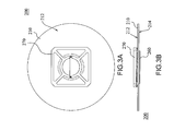
- FIG. 3A is a schematic top view of the test assembly of FIG. 2 after assembled.
- FIG. 3B is a schematic side view of the test assembly of FIG. 2 after assembled.
- FIG. 3C is a schematic bottom view of the test assembly of FIG. 2 after assembled.
- FIG. 3D is a schematic cross-sectional view of partial elements of the assembled test assembly taken along line AA′ of FIG. 3C .
- FIG. 4 is a schematic enlarged perspective view of the test probes of FIG. 2 .
- FIG. 2 is a schematic exploded view of a test assembly according to an embodiment of the present invention.
- FIG. 3A is a schematic top view of the test assembly of FIG. 2 after assembled.
- FIG. 3B is a schematic side view of the test assembly of FIG. 2 after assembled.
- FIG. 3C is a schematic bottom view of the test assembly of FIG. 2 after assembled.
- FIG. 3D is a schematic cross-sectional view of partial elements of the assembled test assembly taken along line AA′ of FIG. 3C .
- a bottom cover and a main stiffener are omitted in FIG. 3D . Referring to FIG. 2 and FIG. 3A through FIG.
- a test assembly 200 is adapted to test a semiconductor device, such as a wafer (not shown).
- the test assembly 200 comprises a main circuit board 210 , an intermediate dielectric board 220 , an intermediate circuit board 230 , a plurality of intermediate conductive elements 240 , a probe base 250 , a bottom cover 260 , a main stiffener 270 , and a plurality of test probes 280 .
- the main circuit board 210 may be connected to an external testing machine (not shown).
- the main circuit board 210 comprises two opposing surfaces 212 , 214 and a plurality of pads 216 (shown in FIG. 3D ).
- the pads 216 are disposed on the surface 214 .
- the main stiffener 270 is disposed on the surface 212 of the main circuit board 210 and fixed to the main circuit board 210 by a plurality of fixing elements 282 , such as bolts.
- the intermediate dielectric board 220 comprises a plurality of through holes 222 .
- the intermediate conductive elements 240 are detachably disposed at the through holes 222 of the intermediate dielectric board 220 , respectively.
- each of the intermediate conductive elements 240 is a pogo pin, for example, and is disposed at one of the through holes 222 in a tight-fit manner.
- the intermediate circuit board 230 comprises a plurality of pads 232 , a plurality of pads 234 , and two opposite surfaces 236 , 238 .
- the pads 232 are disposed on the surface 236 .
- the pads 234 are disposed on the surface 238 .
- the surface 236 of the intermediate circuit board 230 faces the intermediate dielectric board 220 .
- the surface 238 of the intermediate circuit board 230 faces the bottom cover 260 .
- the intermediate dielectric board 220 and the intermediate circuit board 230 are fixed to the bottom cover 260 by means of a plurality of fixing elements 284 , such as bolts, such that the intermediate dielectric board 220 and the intermediate circuit board 230 are detachably disposed at the bottom cover 260 , and the intermediate circuit board 230 is detachably disposed between the intermediate dielectric board 220 and the bottom cover 260 .
- fixing elements 284 such as bolts
- the bottom cover 260 is detachably fixed to a surface 214 of the main circuit board 210 by means of a plurality of fixing elements 286 , such as bolts; hence, the intermediate dielectric board 220 , the intermediate circuit board 230 and the bottom cover 260 are detachably disposed on the surface 214 of the main circuit board 210 , and the intermediate dielectric board 220 is disposed between the intermediate circuit board 230 and the main circuit board 210 . Furthermore, given the aforesaid arrangement, each of the intermediate conductive elements 240 is electrically connected to one of the pads 216 of the main circuit board 210 and one of the pads 232 of the intermediate circuit board 230 .
- FIG. 4 is a schematic enlarged perspective view of the test probes of FIG. 2 .
- the number of the test probes 280 is six, for example.
- Each of the test probes 280 may be a cantilever probe, but the present invention is not limited thereto.
- the test probes 280 are fixed to the probe base 250 by means of a fixing element 252 (such as a resin) and thus supported by the probe base 250 . It should be noted that if each of the test probes 280 is a vertical test probe and the structural strength thereof is sufficient, the probe base 250 can be omitted.
- the probe base 250 is disposed on the surface 238 of the intermediate circuit board 230 and corresponding in position to a through opening 262 of the bottom cover 260 such that the test probes 280 are corresponding in position to the through opening 262 .
- the test probes 280 are disposed on the surface 238 of the intermediate circuit board 230 and electrically connected to the pads 234 of the intermediate circuit board 230 , respectively.
- one end of each of the test probes 280 is connected to one of the pads 234 of the intermediate circuit board 230 by means of soldering.
- each of the test probes 280 is electrically connected to the main circuit board 210 through the intermediate circuit board 230 and one of the intermediate conductive elements 240 . Furthermore, another end of each of the test probes 280 is adapted to electrically contact a semiconductor device in order to test the semiconductor device. Specifically speaking, the main circuit board 210 receives test signals from the testing machine. The test signals are transmitted through the test probes 280 such that an electrical test is performed on the semiconductor device.
- the test assembly 200 comprises the main circuit board 210 and the intermediate circuit board 230 , and the intermediate conductive elements 240 and the intermediate circuit board 230 can serve the medium of electrical connection between the main circuit board 210 and the test probes 240 , so compared to the prior art, the circuit design of the main circuit board 210 can be simplified such that the volume of the main circuit board 210 can be reduced. Therefore, in this embodiment, the required space occupied by the main circuit board 210 of the test assembly 200 can decrease. Furthermore, if the circuit of the main circuit board 210 is defective and thus the main circuit board 210 must be replaced, the cost of replacing the main circuit board 210 having the simple circuit is relatively low.
- the intermediate dielectric board 220 , the intermediate conductive elements 240 , the intermediate circuit board 230 , the bottom cover 260 , the probe base 250 and the test probes 280 can be put together to form a sub-assembly in advance. Then, the sub-assembly and the main stiffener 270 are respectively mounted on the two opposite surfaces 214 , 212 of the main circuit board to form the test assembly 200 of this embodiment.
- each of the intermediate conductive elements 240 can be a pogo pin and the sub-assembly formed from the intermediate dielectric board 220 , the intermediate conductive elements 240 , the intermediate circuit board 230 , the bottom cover 260 , the probe base 250 and the test probes 280 in advance is detachably disposed on the main circuit board 210 , the detachment of the sub-assembly from the main circuit board 210 is easy whenever the main circuit board 210 of which the circuit is defective must be replaced.
- the test assembly of the aforementioned embodiment of the present invention has one of the following advantages or another advantage.
- the test assembly of the embodiment of the present invention comprises the main circuit board and the intermediate circuit board, and the intermediate conductive elements and the intermediate circuit board can serve the medium of electrical connection between the main circuit board and the test probes, so compared to the prior art, the circuit design of the main circuit board can be simplified such that the volume of the main circuit board can be reduced. Therefore, the required space occupied by the main circuit board of the test assembly of the embodiment of the present invention can decrease. Furthermore, if the circuit of the main circuit board is defective and thus the main circuit board must be replaced, the cost of replacing the main circuit board having the simple circuit is relatively low.
- each of the intermediate conductive elements can be a pogo pin and the sub-assembly formed from the intermediate dielectric board, the intermediate conductive elements, the intermediate circuit board, the bottom cover and the test probes in advance is detachably disposed on the main circuit board, the detachment of the sub-assembly from the main circuit board is easy whenever the main circuit board of which the circuit is defective must be replaced.
Landscapes
- Physics & Mathematics (AREA)
- General Physics & Mathematics (AREA)
- Engineering & Computer Science (AREA)
- Computer Hardware Design (AREA)
- Microelectronics & Electronic Packaging (AREA)
- General Engineering & Computer Science (AREA)
- Testing Or Measuring Of Semiconductors Or The Like (AREA)
- Testing Of Individual Semiconductor Devices (AREA)
Abstract
Description
Claims (18)
Applications Claiming Priority (3)
| Application Number | Priority Date | Filing Date | Title |
|---|---|---|---|
| TW102209078 | 2013-05-15 | ||
| TW102209078U TWM463903U (en) | 2013-05-15 | 2013-05-15 | Test assembly |
| TW102209078U | 2013-05-15 |
Publications (2)
| Publication Number | Publication Date |
|---|---|
| US20140340105A1 US20140340105A1 (en) | 2014-11-20 |
| US9739830B2 true US9739830B2 (en) | 2017-08-22 |
Family
ID=49773012
Family Applications (1)
| Application Number | Title | Priority Date | Filing Date |
|---|---|---|---|
| US14/275,783 Active 2034-09-19 US9739830B2 (en) | 2013-05-15 | 2014-05-12 | Test assembly |
Country Status (4)
| Country | Link |
|---|---|
| US (1) | US9739830B2 (en) |
| JP (1) | JP3192062U (en) |
| KR (1) | KR200478467Y1 (en) |
| TW (1) | TWM463903U (en) |
Families Citing this family (4)
| Publication number | Priority date | Publication date | Assignee | Title |
|---|---|---|---|---|
| TWI604198B (en) | 2016-06-22 | 2017-11-01 | 思達科技股份有限公司 | Testing apparatus, holding assembly, and probe card carrier |
| CN114137384B (en) * | 2020-09-04 | 2025-01-24 | 思达科技股份有限公司 | Test equipment |
| KR102454947B1 (en) * | 2020-11-05 | 2022-10-17 | 주식회사 에스디에이 | Probe card |
| TWI837548B (en) * | 2021-11-18 | 2024-04-01 | 致茂電子股份有限公司 | Component inspection jig |
Citations (8)
| Publication number | Priority date | Publication date | Assignee | Title |
|---|---|---|---|---|
| US6917102B2 (en) * | 2002-10-10 | 2005-07-12 | Advantest Corp. | Contact structure and production method thereof and probe contact assembly using same |
| US20060006889A1 (en) | 2004-07-07 | 2006-01-12 | Kenneth Smith | Probe head having a membrane suspended probe |
| US7009412B2 (en) * | 1999-05-27 | 2006-03-07 | Nanonexus, Inc. | Massively parallel interface for electronic circuit |
| US20070046304A1 (en) * | 2000-05-23 | 2007-03-01 | Sammy Mok | Construction Structures and Manufacturing Processes for Integrated Circuit Wafer Probe Card Assemblies |
| US20080100291A1 (en) * | 2006-10-26 | 2008-05-01 | Silicon Test Systems, Inc. | Solid high aspect ratio via hole used for burn-in boards, wafer sort probe cards, and package test load boards with electronic circuitry |
| KR20080082670A (en) | 2005-12-05 | 2008-09-11 | 니혼 하츠쵸 가부시키가이샤 | Probe card |
| US20100237889A1 (en) * | 2009-02-19 | 2010-09-23 | Touchdown Technologies, Inc. | Probe head for a microelectronic contactor assembly, the probe head having smt electronic components thereon |
| US20140077833A1 (en) * | 2012-09-19 | 2014-03-20 | Mpi Corporation | Probe card and manufacturing method thereof |
-
2013
- 2013-05-15 TW TW102209078U patent/TWM463903U/en not_active IP Right Cessation
-
2014
- 2014-05-12 US US14/275,783 patent/US9739830B2/en active Active
- 2014-05-14 JP JP2014002478U patent/JP3192062U/en not_active Expired - Lifetime
- 2014-05-15 KR KR2020140003750U patent/KR200478467Y1/en not_active Expired - Lifetime
Patent Citations (10)
| Publication number | Priority date | Publication date | Assignee | Title |
|---|---|---|---|---|
| US7009412B2 (en) * | 1999-05-27 | 2006-03-07 | Nanonexus, Inc. | Massively parallel interface for electronic circuit |
| US20070046304A1 (en) * | 2000-05-23 | 2007-03-01 | Sammy Mok | Construction Structures and Manufacturing Processes for Integrated Circuit Wafer Probe Card Assemblies |
| US6917102B2 (en) * | 2002-10-10 | 2005-07-12 | Advantest Corp. | Contact structure and production method thereof and probe contact assembly using same |
| US20060006889A1 (en) | 2004-07-07 | 2006-01-12 | Kenneth Smith | Probe head having a membrane suspended probe |
| KR20070053696A (en) | 2004-07-07 | 2007-05-25 | 캐스케이드 마이크로테크 인코포레이티드 | Probe head with membrane suspended probe |
| KR20080082670A (en) | 2005-12-05 | 2008-09-11 | 니혼 하츠쵸 가부시키가이샤 | Probe card |
| US20100052707A1 (en) | 2005-12-05 | 2010-03-04 | Nhk Spring Co.,Ltd | Probe Card |
| US20080100291A1 (en) * | 2006-10-26 | 2008-05-01 | Silicon Test Systems, Inc. | Solid high aspect ratio via hole used for burn-in boards, wafer sort probe cards, and package test load boards with electronic circuitry |
| US20100237889A1 (en) * | 2009-02-19 | 2010-09-23 | Touchdown Technologies, Inc. | Probe head for a microelectronic contactor assembly, the probe head having smt electronic components thereon |
| US20140077833A1 (en) * | 2012-09-19 | 2014-03-20 | Mpi Corporation | Probe card and manufacturing method thereof |
Also Published As
| Publication number | Publication date |
|---|---|
| KR200478467Y1 (en) | 2015-10-08 |
| KR20140005951U (en) | 2014-11-26 |
| US20140340105A1 (en) | 2014-11-20 |
| JP3192062U (en) | 2014-07-24 |
| TWM463903U (en) | 2013-10-21 |
Similar Documents
| Publication | Publication Date | Title |
|---|---|---|
| JP6395936B2 (en) | Test socket | |
| US10119995B2 (en) | Probe card | |
| US8901920B2 (en) | Connector, probe, and method of manufacturing probe | |
| US20140210504A1 (en) | Testing device for electronic device testing | |
| KR20160092366A (en) | Pin block and test appartus with the same | |
| US9739830B2 (en) | Test assembly | |
| CN104422863A (en) | Semiconductor testing device | |
| KR20130047933A (en) | Probe, probe assembly and probe card comprising it | |
| KR101626513B1 (en) | Semiconductor chip test socket | |
| CN102208732B (en) | connecting device | |
| KR101337427B1 (en) | A Probe For Testing the Semiconductor | |
| KR20220036784A (en) | Jig for PCB inspection | |
| JP5865846B2 (en) | Inspection socket | |
| CN109270299B (en) | Circuit rotating plate integrating thin film circuit board and spring needle | |
| US20120169366A1 (en) | Socket contact for testing a semiconductor | |
| KR101041219B1 (en) | Contact module for inspection | |
| JP2010043868A (en) | Electric inspection jig and electric inspection apparatus | |
| KR102037924B1 (en) | Test tray for using test handler | |
| KR101680319B1 (en) | Probe block for testing a liquid crystal panel | |
| KR20140002790U (en) | Insert assembly for testing a semiconductor device | |
| TWI684772B (en) | Inspecting device and its socket | |
| KR102065602B1 (en) | Socket of test board | |
| KR101981526B1 (en) | U-type PION pin of test scoket | |
| US9553386B2 (en) | Contact | |
| US10386407B2 (en) | Socket |
Legal Events
| Date | Code | Title | Description |
|---|---|---|---|
| AS | Assignment |
Owner name: STAR TECHNOLOGIES, INC., TAIWAN Free format text: ASSIGNMENT OF ASSIGNORS INTEREST;ASSIGNORS:LOU, CHOON LEONG;TSENG, HSIAO TING;CHEN, HO YEH;AND OTHERS;SIGNING DATES FROM 20140505 TO 20140506;REEL/FRAME:032873/0162 |
|
| STCF | Information on status: patent grant |
Free format text: PATENTED CASE |
|
| MAFP | Maintenance fee payment |
Free format text: PAYMENT OF MAINTENANCE FEE, 4TH YR, SMALL ENTITY (ORIGINAL EVENT CODE: M2551); ENTITY STATUS OF PATENT OWNER: SMALL ENTITY Year of fee payment: 4 |
|
| FEPP | Fee payment procedure |
Free format text: ENTITY STATUS SET TO UNDISCOUNTED (ORIGINAL EVENT CODE: BIG.); ENTITY STATUS OF PATENT OWNER: LARGE ENTITY |
|
| MAFP | Maintenance fee payment |
Free format text: PAYMENT OF MAINTENANCE FEE UNDER 1.28(C) (ORIGINAL EVENT CODE: M1559); ENTITY STATUS OF PATENT OWNER: LARGE ENTITY |
|
| FEPP | Fee payment procedure |
Free format text: PETITION RELATED TO MAINTENANCE FEES GRANTED (ORIGINAL EVENT CODE: PTGR); ENTITY STATUS OF PATENT OWNER: LARGE ENTITY |
|
| MAFP | Maintenance fee payment |
Free format text: PAYMENT OF MAINTENANCE FEE, 8TH YEAR, LARGE ENTITY (ORIGINAL EVENT CODE: M1552); ENTITY STATUS OF PATENT OWNER: LARGE ENTITY Year of fee payment: 8 |