US9729044B2 - Power conversion device having two serially-connected switching elements - Google Patents
Power conversion device having two serially-connected switching elements Download PDFInfo
- Publication number
- US9729044B2 US9729044B2 US14/915,290 US201414915290A US9729044B2 US 9729044 B2 US9729044 B2 US 9729044B2 US 201414915290 A US201414915290 A US 201414915290A US 9729044 B2 US9729044 B2 US 9729044B2
- Authority
- US
- United States
- Prior art keywords
- power conversion
- conversion device
- elements
- terminal
- element modules
- Prior art date
- Legal status (The legal status is an assumption and is not a legal conclusion. Google has not performed a legal analysis and makes no representation as to the accuracy of the status listed.)
- Active
Links
Images


Classifications
-
- H—ELECTRICITY
- H02—GENERATION; CONVERSION OR DISTRIBUTION OF ELECTRIC POWER
- H02M—APPARATUS FOR CONVERSION BETWEEN AC AND AC, BETWEEN AC AND DC, OR BETWEEN DC AND DC, AND FOR USE WITH MAINS OR SIMILAR POWER SUPPLY SYSTEMS; CONVERSION OF DC OR AC INPUT POWER INTO SURGE OUTPUT POWER; CONTROL OR REGULATION THEREOF
- H02M1/00—Details of apparatus for conversion
- H02M1/32—Means for protecting converters other than automatic disconnection
- H02M1/34—Snubber circuits
-
- H—ELECTRICITY
- H02—GENERATION; CONVERSION OR DISTRIBUTION OF ELECTRIC POWER
- H02M—APPARATUS FOR CONVERSION BETWEEN AC AND AC, BETWEEN AC AND DC, OR BETWEEN DC AND DC, AND FOR USE WITH MAINS OR SIMILAR POWER SUPPLY SYSTEMS; CONVERSION OF DC OR AC INPUT POWER INTO SURGE OUTPUT POWER; CONTROL OR REGULATION THEREOF
- H02M7/00—Conversion of AC power input into DC power output; Conversion of DC power input into AC power output
- H02M7/003—Constructional details, e.g. physical layout, assembly, wiring or busbar connections
-
- H—ELECTRICITY
- H02—GENERATION; CONVERSION OR DISTRIBUTION OF ELECTRIC POWER
- H02M—APPARATUS FOR CONVERSION BETWEEN AC AND AC, BETWEEN AC AND DC, OR BETWEEN DC AND DC, AND FOR USE WITH MAINS OR SIMILAR POWER SUPPLY SYSTEMS; CONVERSION OF DC OR AC INPUT POWER INTO SURGE OUTPUT POWER; CONTROL OR REGULATION THEREOF
- H02M7/00—Conversion of AC power input into DC power output; Conversion of DC power input into AC power output
- H02M7/42—Conversion of DC power input into AC power output without possibility of reversal
- H02M7/44—Conversion of DC power input into AC power output without possibility of reversal by static converters
- H02M7/48—Conversion of DC power input into AC power output without possibility of reversal by static converters using discharge tubes with control electrode or semiconductor devices with control electrode
- H02M7/53—Conversion of DC power input into AC power output without possibility of reversal by static converters using discharge tubes with control electrode or semiconductor devices with control electrode using devices of a triode or transistor type requiring continuous application of a control signal
- H02M7/537—Conversion of DC power input into AC power output without possibility of reversal by static converters using discharge tubes with control electrode or semiconductor devices with control electrode using devices of a triode or transistor type requiring continuous application of a control signal using semiconductor devices only, e.g. single switched pulse inverters
-
- H—ELECTRICITY
- H05—ELECTRIC TECHNIQUES NOT OTHERWISE PROVIDED FOR
- H05K—PRINTED CIRCUITS; CASINGS OR CONSTRUCTIONAL DETAILS OF ELECTRIC APPARATUS; MANUFACTURE OF ASSEMBLAGES OF ELECTRICAL COMPONENTS
- H05K7/00—Constructional details common to different types of electric apparatus
- H05K7/20—Modifications to facilitate cooling, ventilating, or heating
- H05K7/2089—Modifications to facilitate cooling, ventilating, or heating for power electronics, e.g. for inverters for controlling motor
- H05K7/209—Heat transfer by conduction from internal heat source to heat radiating structure
-
- H01L2224/05554—
-
- H01L2224/40137—
-
- H01L2224/48247—
-
- H01L2924/00012—
-
- H01L2924/181—
-
- H—ELECTRICITY
- H02—GENERATION; CONVERSION OR DISTRIBUTION OF ELECTRIC POWER
- H02M—APPARATUS FOR CONVERSION BETWEEN AC AND AC, BETWEEN AC AND DC, OR BETWEEN DC AND DC, AND FOR USE WITH MAINS OR SIMILAR POWER SUPPLY SYSTEMS; CONVERSION OF DC OR AC INPUT POWER INTO SURGE OUTPUT POWER; CONTROL OR REGULATION THEREOF
- H02M1/00—Details of apparatus for conversion
- H02M1/32—Means for protecting converters other than automatic disconnection
- H02M1/34—Snubber circuits
- H02M1/348—Passive dissipative snubbers
-
- H02M2001/348—
-
- H—ELECTRICITY
- H10—SEMICONDUCTOR DEVICES; ELECTRIC SOLID-STATE DEVICES NOT OTHERWISE PROVIDED FOR
- H10W—GENERIC PACKAGES, INTERCONNECTIONS, CONNECTORS OR OTHER CONSTRUCTIONAL DETAILS OF DEVICES COVERED BY CLASS H10
- H10W72/00—Interconnections or connectors in packages
- H10W72/60—Strap connectors, e.g. thick copper clips for grounding of power devices
- H10W72/651—Materials of strap connectors
- H10W72/652—Materials of strap connectors comprising metals or metalloids, e.g. silver
-
- H—ELECTRICITY
- H10—SEMICONDUCTOR DEVICES; ELECTRIC SOLID-STATE DEVICES NOT OTHERWISE PROVIDED FOR
- H10W—GENERIC PACKAGES, INTERCONNECTIONS, CONNECTORS OR OTHER CONSTRUCTIONAL DETAILS OF DEVICES COVERED BY CLASS H10
- H10W72/00—Interconnections or connectors in packages
- H10W72/90—Bond pads, in general
- H10W72/921—Structures or relative sizes of bond pads
- H10W72/926—Multiple bond pads having different sizes
-
- H—ELECTRICITY
- H10—SEMICONDUCTOR DEVICES; ELECTRIC SOLID-STATE DEVICES NOT OTHERWISE PROVIDED FOR
- H10W—GENERIC PACKAGES, INTERCONNECTIONS, CONNECTORS OR OTHER CONSTRUCTIONAL DETAILS OF DEVICES COVERED BY CLASS H10
- H10W72/00—Interconnections or connectors in packages
- H10W72/90—Bond pads, in general
- H10W72/931—Shapes of bond pads
- H10W72/932—Plan-view shape, i.e. in top view
-
- H—ELECTRICITY
- H10—SEMICONDUCTOR DEVICES; ELECTRIC SOLID-STATE DEVICES NOT OTHERWISE PROVIDED FOR
- H10W—GENERIC PACKAGES, INTERCONNECTIONS, CONNECTORS OR OTHER CONSTRUCTIONAL DETAILS OF DEVICES COVERED BY CLASS H10
- H10W74/00—Encapsulations, e.g. protective coatings
-
- H—ELECTRICITY
- H10—SEMICONDUCTOR DEVICES; ELECTRIC SOLID-STATE DEVICES NOT OTHERWISE PROVIDED FOR
- H10W—GENERIC PACKAGES, INTERCONNECTIONS, CONNECTORS OR OTHER CONSTRUCTIONAL DETAILS OF DEVICES COVERED BY CLASS H10
- H10W90/00—Package configurations
- H10W90/701—Package configurations characterised by the relative positions of pads or connectors relative to package parts
- H10W90/751—Package configurations characterised by the relative positions of pads or connectors relative to package parts of bond wires
- H10W90/756—Package configurations characterised by the relative positions of pads or connectors relative to package parts of bond wires between a chip and a stacked lead frame, conducting package substrate or heat sink
-
- H—ELECTRICITY
- H10—SEMICONDUCTOR DEVICES; ELECTRIC SOLID-STATE DEVICES NOT OTHERWISE PROVIDED FOR
- H10W—GENERIC PACKAGES, INTERCONNECTIONS, CONNECTORS OR OTHER CONSTRUCTIONAL DETAILS OF DEVICES COVERED BY CLASS H10
- H10W90/00—Package configurations
- H10W90/701—Package configurations characterised by the relative positions of pads or connectors relative to package parts
- H10W90/761—Package configurations characterised by the relative positions of pads or connectors relative to package parts of strap connectors
- H10W90/763—Package configurations characterised by the relative positions of pads or connectors relative to package parts of strap connectors between laterally-adjacent chips
Definitions
- the present disclosure relates to a power conversion device which includes two serially-connected switching elements (hereinafter, referred to as the SW elements) of an upper arm and a lower arm and supplies power to a load from a connection point of the two SW elements by converting a voltage and a current from a DC power supply.
- the SW elements serially-connected switching elements
- a power conversion device which includes two serially-connected SW elements of an upper arm and a lower arm and supplies power to a load by converting a voltage and a current from a DC power supply is disclosed, for example, in JP2005-287267A (Patent Literature 1).
- a power conversion device employed in a vehicle is required to have high power density (compact size and large current) and a small power loss.
- a current, a voltage, and a switching speed (hereinafter, referred to as a SW speed) of the SW elements are kept increased.
- a surge voltage occurring at the time of switching is increased.
- a switching loss hereinafter, referred to as a SW loss
- the surge voltage also depends on a value of floating inductance in an interior of a filter capacitor or a power module forming the power conversion device or in a bus bar electrically connecting the foregoing components, and the surge voltage becomes high when the floating inductance is large.
- the power conversion device disclosed in Patent Literature 1 includes power modules in each of which the SW element is molded with resin in the shape of a flat rectangular parallelepiped.
- a positive electrode and a negative electrode are provided on one flat surface of the power module and the other surface forming a heat-sinking plane is connected to a cooling substrate.
- a positive (upper arm) power module group and a negative (lower arm) power module group are disposed in such a manner that the respective surfaces provided with the electrodes oppose each other at a predetermined interval and form a two-way path in which currents flowing in and out from the respective modules oppose each other. Owing to the location and the configuration of the power modules as above, the power conversion device of Patent Literature 1 restricts a surge voltage to be low by reducing the floating inductance occurring between the power modules.
- the SW element disclosed in Patent Literature 2 is a double-sided heat-sinking element module.
- the element module has a structure in which a pair of heat sinks is bonded to both surfaces of a semiconductor chip, for example, via solder layers, and the element module is entirely molded with resin in such a manner that respective outer surfaces of a pair of the heat sinks are exposed. Accordingly, heat can be released from the both surfaces of the semiconductor chip and high radiation performance can be exerted.
- the element module of Patent Literature 2 is also shaped like a flat rectangular parallelepiped. However, different from the power module in Patent Literature 1, the heat sink exposed to one flat surface forms a positive electrode and the heat sink exposed to the other surface forms a negative electrode.
- Patent Literature 1 JP2005-287267A
- Patent Literature 2 JP2003-110064A
- a power conversion device employed in a vehicle or the like is required to have high power density and a small power loss. Accordingly, restriction of a surge voltage becomes a problem as a current, a voltage, and a SW speed of the SW elements are increased. In addition, radiation performance of the SW elements needs to be increased as a current becomes larger. Further, in order to ensure EMC, not only a surge voltage but also ringing, which becomes FM band noises accompanying the surge voltage, has to be restricted.
- the present disclosure is directed to a power conversion device which includes two serially-connected SW elements of an upper arm and a lower arm and supplies power to a load from a connection point of the two SW elements by converting a voltage and a current from a DC power supply.
- the present disclosure has an object to provide a power conversion device capable of achieving three requirements to restrict a surge voltage, ensure high radiation performance of SW elements, and restrict ringing.
- a power conversion device includes two serially-connected SW elements of an upper and a lower arm and supplies power to a load from a connection point of the two SW elements by converting a voltage and a current from a DC power supply.
- Each of the two SW elements is provided by an element module which is molded with resin in a shape of a flat rectangular parallelepiped.
- a heat sink connected to a positive electrode of the SW element is disposed on a flat surface of the rectangular parallelepiped and a heat sink connected to a negative electrode of the SW element is disposed on an opposite flat surface of the rectangular parallelepiped in such a manner that outer surfaces of the heat sinks are exposed.
- a positive terminal coupled to the heat sink connected to the positive electrode and a negative terminal coupled to the heat sink connected to the negative electrode are extracted from a lateral surface of the flat rectangular parallelepiped so as not to overlap in a thickness direction of the rectangular parallelepiped.
- the element modules of the two SW elements are stacked in the thickness direction via an insulating layer in such a manner that the lateral surface of one of the two SW elements and the lateral surface of the other of the two SW elements, from each of which the positive terminal and the negative terminal are extracted, are aligned parallel to each other in a same orientation.
- the positive terminal of the one of the SW elements and the negative terminal of the other of the SW elements are disposed so as to overlap each other in the thickness direction.
- the positive terminal and the negative terminal are electrically connected in a vicinity of the lateral surfaces of the two SW elements to provide an output terminal (hereinafter, referred to as the O terminal) connected to the load.
- the positive terminal of the SW element of the upper arm provides a high-potential terminal (hereinafter, referred to as the P terminal) to be connected to a high potential side of the DC power supply and the negative terminal of the SW element of the lower arm provides a low-potential terminal (hereinafter, referred to as the N terminal) to be connected to a low potential side of the DC power supply.
- the P terminal high-potential terminal
- the N terminal low-potential terminal
- the power conversion device adopts a double-sided heat-sinking element module as follows. That is, the two serially-connected SW elements of the upper arm and the lower arm are formed of the element modules molded with resin in the shape of a flat rectangular parallelepiped. Also, the element modules have a structure in which the heat sink connected to the positive electrode of the SW element is disposed on the one flat surface of the rectangular parallelepiped and the heat sink connected to the negative electrode is disposed on the opposite flat surface in such a manner that the respective outer surfaces are exposed.
- the double-sided heat-sinking element modules as the SW elements, high radiation performance can be exerted in comparison, for example, with a single-sided heat-sinking element module in which a heat sink is disposed on only one surface of the flat rectangular parallelepiped.
- the element modules are the SW elements of the upper arm and the lower arm, which are separately molded with resin.
- the element modules are compact modules in comparison, for example, with a module in which two SW elements of the upper arm and the lower arm are integrally molded with resin or a module in which three SW elements corresponding to respective three phases U, V, and W of the upper arms are integrally molded with resin. Consequently, in a case where the two element modules described below are stacked, the two element modules can be attached at a high degree of accuracy, and even when a temperature rises due to heat generated in the SW elements, deformation caused by warpage or the like becomes smaller.
- each element module has a structure in which the positive terminal coupled to the heat sink connected to the positive electrode of the SW element and the negative terminal coupled to the heat sink connected to the negative electrode are extracted from a lateral surface of the flat rectangular parallelepiped so as not to overlap each other in the thickness direction of the rectangular parallelepiped.
- the two element modules corresponding to the SW elements of the upper arm and the lower arm are stacked in the thickness direction via the insulating layer in such a manner that the lateral surface of the one of the two SW elements and the lateral surface of the other of the two SW elements, from each of which the positive terminal and the negative terminal are extracted, are aligned parallel to each other in the same orientation.
- the positive terminal of the one of the two SW elements and the negative terminal of the other of the two SW elements are disposed so as to overlap each other in the thickness direction. That is to say, the positive terminal and the negative terminal are in a locational relation such that the positive terminal and the negative terminal overlap at least partially when projected onto one plane in the thickness direction of the flat rectangular parallelepiped.
- the positive terminal and the negative terminal are electrically connected in the vicinity of the lateral surfaces of the two SW elements to provide the O terminal to be connected to the load.
- the positive terminal of the SW element of the upper arm provides the P terminal to be connected to a high potential side of the DC power supply and the negative terminal of the SW element of the lower arm provides the N terminal to be connected to a low potential side of the DC power supply.
- the locational relation of the two element modules forming the power conversion device is aimed at restricting a surge voltage ⁇ V by making inductance Ld of a power-supply circuit smaller. That is to say, in the other set of the positive terminal and the negative terminal disposed so as to overlap, a current flows in an opposite direction at the positive terminal of the SW element of the upper arm forming the P terminal and at the negative terminal of the SW element of the lower arm forming the N terminal. Hence, an effect of reducing inductance by cancelling out magnetic fluxes is exerted. In the one set, too, a current flows in an opposite direction also at the negative terminal of the SW element of the upper arm and the positive terminal of the SW element of the lower arm until the both are electrically connected to form the O terminal.
- the inductance reducing effect obtained by canceling out magnetic fluxes is exerted as well.
- the power conversion device becomes capable of restricting the surge voltage ⁇ V by making the inductance Ld of the power-supply circuit in the power conversion device smaller.
- magnetic energy stored in the inductance Ld is reduced.
- resonance with a latent parasitic capacitance component in an Ld path is damped early and a period during which ringing occurs can be shortened.
- the two element modules forming the power conversion device are compact modules in which the SW elements of the upper arm and the lower arm are molded separately with resin, and can be attached at a high degree of accuracy. Even when a temperature rises due to heat generated in the SW elements, deformation caused by warpage becomes smaller. In particular, deformation of a metal material, such as the electrodes, becomes smaller, too. Hence, the inductance reducing effect obtained by cancelling out magnetic fluxes described above can be exerted in a reliable manner between the positive terminal of the one of the two SW elements and the negative terminal of the other of the two SW elements. In the event of failure in one of the two SW elements due to poor manufacturing or heat generation, only the failed element module has to be replaced. Hence, a fabrication yield and a service life of the power conversion device can be improved.
- the power conversion device is configured in such a manner that the positive terminal and the negative terminal disposed so as to overlap are in a locational relation such that either one terminal covers the other in the thickness direction. That is to say, the positive terminal and the negative terminal are in a locational relation such that one covers the other when projected onto one plane in the thickness direction of the flat rectangular parallelepiped.
- the positive terminal and the negative terminal are of an identical shape, the positive terminal and the negative terminal are in a locational relation such that the both coincide perfectly when projected onto one plane in the thickness direction of the flat rectangular parallelepiped.
- the element modules of the two SW elements corresponding to the respective upper and lower arms in the power conversion device are of a same structure. This configuration is preferable not only from the viewpoint of matching the characteristics of the SW elements and reducing the manufacturing costs, but also from the viewpoint of restricting a surge voltage.
- the positive terminal and the negative terminal are extracted from the lateral surface of each element module of the power conversion device at a same height in the thickness direction. Consequently, a design and attachment becomes easier.
- the positive terminal and the negative terminal are extracted from one of two regions divided in the thickness direction by a bisector.
- the positive terminal and the negative terminal in the locational relation to overlap each other can be disposed in closer proximity to each other in comparison with the element modules from which the corresponding positive terminal and negative terminal are extracted from positions on a bisector (center) in the thickness direction.
- the power conversion device is configured in such a manner that in the other set of the positive electrode forming the P terminal and the negative electrode forming the N terminal, a snubber circuit having a capacitor element can be electrically connected adjacent to the lateral surfaces of the two SW elements between the positive element and the negative electrode.
- the surge voltage ⁇ V can be reduced further by letting a capacitor element of the snubber circuit absorb energy accumulated in the inductance Ld of the power supply circuit.
- the snubber circuit in the power conversion device is to connect the P and N terminals of the two stacked element modules with a separate member other than the element modules, and is therefore exposed to the outside of the element modules. Hence, heat generated in the snubber circuit can be released satisfactorily in a radiation path different from a radiation path of heat generated in the SW elements via the heat sinks coupled to the positive terminal and the negative terminal extracted to the outside and by means of heat dissipation to air.
- the snubber circuit in the power conversion device may include a metal member having a current path with substantially a U-shape between the positive terminal and the negative terminal and provided with a cut portion at a midpoint, and a surface-mounted capacitor element, electrodes of which are connected to opposite sides of the cut portion.
- a resistor is connected to the capacitor element in series in the snubber circuit.
- a resistance value Rs of the resistor connected to the capacitor element in series has an appropriate value.
- the resistance value Rs is too small, a surge that needs to be reduced cannot be restricted. A current is not consumed by parasitic inductance and the capacitor element in the snubber circuit alone (current is stored in the parasitic inductance) and a resistor that consumes the current becomes necessary. Also, the LC resonance described above occurs readily, which becomes another problem. Conversely, when the resistance value Rs is too large, a surge occurring in the SW elements is not bypassed to the snubber circuit side and the snubber circuit no longer functions.
- the resistor connected to the capacitor element in series may be formed of a surface-mounted resistor element, and electrodes of the resistor may be connected to opposite sides of a cut portion provided to the metal member of substantially U shape at a position different from the cut portion to which the capacitor element is connected.
- the resistor may be formed of a trimmed resistor portion, a sectional area of which is reduced at a midpoint of the current path by making an incision to the metal member of substantially a U shape.
- the resistor may be formed by combining the surface-mounted resistor element and the trimmed resistor portion. When the trimmed resistor portion is used as the resistor, the resistance value Rs can be adjusted after the snubber circuit is attached to the power conversion device.
- the snubber circuit in the power conversion device described above is electrically connected collectively between the P terminal of the element module of the upper arm and the N terminal of the element module of the lower arm stacked one on the other.
- a configuration of the snubber circuit is not limited to the configuration described above.
- the snubber circuit may be electrically connected between the positive terminal and the negative terminal individually in each of the stacked element modules of the upper arm and the lower arm.
- the snubber circuit in the power conversion device described above is a C snubber circuit having a capacitor alone or an RC snubber circuit having a capacitor element and a resistor.
- a configuration of the snubber circuit is not limited to the configurations as above and the snubber circuit may be an RCD snubber circuit in which a diode is connected to a resistor in parallel.
- the power conversion device adopts double-sided heat-sinking element modules.
- the power conversion device may be configured in such a manner that the element modules of the two SW elements are disposed between water-cooling coolers via an insulating layer.
- heat generated in the SW elements heat generated in the capacitor element and the resistor when the snubber circuit is connected
- the water-cooling coolers from the heat sinks exposed to the outer surfaces of the respective element modules via the insulating layer. Consequently, a high cooling effect can be exerted.
- the power conversion device described above is a power conversion device capable of achieving three requirements to restrict a surge voltage, ensure high radiation performance of SW elements, and restrict ringing at the same time.
- the power conversion device described above can be employed in a vehicle for which a power conversion device having high power density and a small power loss is required and restriction of a surge voltage becomes a problem when a current, a voltage, and a SW speed of the SW elements are increased.
- FIG. 1A is a front view of an element module of a SW element used in a power conversion device according to an embodiment of the present disclosure
- FIG. 1B is a bottom view of the element module shown in FIG. 1A to see through an interior;
- FIG. 1C is a sectional view taken along the alternate long and short dash line IC-IC of FIG. 1B ;
- FIG. 2A is a circuit diagram showing an example of a configuration and a usage pattern of the power conversion device according to the embodiment of the present disclosure
- FIG. 2B is a perspective view showing an outward appearance of the power conversion device shown in FIG. 2A ;
- FIG. 2C is a schematic front view of the power conversion device when viewed in a direction indicated by an arrow A of FIG. 2B ;
- FIG. 3A is a perspective view showing an outward appearance of a modification of the power conversion device
- FIG. 3B is a perspective view showing an outward appearance of another modification of the power conversion device
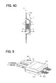
- FIG. 4A is a front view showing an example of another element module
- FIG. 4B is a bottom view of the element module shown in FIG. 4A to see through an interior;
- FIG. 4C is a sectional view taken along the alternate long and short dash line IVC-IVC of FIG. 4B ;
- FIG. 5 is a perspective view showing an outward appearance of a power conversion device using the element module of FIG. 4A through FIG. 4C ;
- FIG. 6A is a sectional view of a power conversion device showing another example of the configuration of the power conversion device using the element module shown in FIG. 1A through FIG. 1C ;
- FIG. 6B is a sectional view of a power conversion device showing another example of the configuration of the power conversion device using the element module shown in FIG. 4A through FIG. 4C ;
- FIG. 7A is a circuit diagram showing an example of a configuration and a usage pattern of a power conversion device additionally provided with a snubber circuit
- FIG. 7B is a perspective view showing an outward appearance of the power conversion device shown in FIG. 7A ;
- FIG. 7C is a schematic front view of the power conversion device when viewed in a direction indicated by an arrow A of FIG. 7B ;
- FIG. 8A is a perspective view showing an outward appearance of still another example of the power conversion device.
- FIG. 8B is a front view of the power conversion device shown in FIG. 8A when viewed in a direction indicated by an arrow A;
- FIG. 8C is an enlarged view of the snubber circuit in the power conversion device shown in FIG. 8B ;
- FIG. 9A is a top view showing another example of an actual configuration of the snubber circuit in the middle of fabrication
- FIG. 9B is a front view of the snubber circuit shown in FIG. 9A ;
- FIG. 9C is an enlarged front view of the completed snubber circuit shown in FIG. 9B ;
- FIG. 10A is a top view showing still another example of the actual configuration of the snubber circuit during fabrication
- FIG. 10B is a front view of the snubber circuit shown in FIG. 10A ;
- FIG. 10C is an enlarged front view of the completed snubber circuit shown in FIG. 10B ;
- FIG. 11A is a schematic view of a power conversion device, which is the power conversion device shown in FIG. 6A provided with the snubber circuit;
- FIG. 11B is a schematic view of a power conversion device, which is the power conversion device shown in FIG. 6B provided with the snubber circuit;
- FIG. 12 is a top view of an inverter using an in-vehicle three-phase motor as a load, which is an example application of the power conversion device shown in FIG. 11A or FIG. 11B .
- a power conversion device of the present disclosure includes two serially-connected SW elements of an upper arm and a lower arm and supplies power to a load from a connection point of the two SW elements by converting a voltage and a current from a DC power supply.
- FIG. 1A through FIG. 1C are views showing an example of an element module of a SW element used in the power conversion device of the present disclosure.
- FIG. 1A is a front view of an element module 10 .
- FIG. 1B is a bottom view of the element module 10 to see through an interior.
- FIG. 1C is a sectional view taken along the alternate long and short dash line IC-IC of FIG. 1B .
- FIG. 2A through FIG. 2C show an example of the power conversion device of the present disclosure using the SW element (element module 10 ) of FIG. 1A through FIG. 1C .
- FIG. 2A is a circuit diagram showing an example of a configuration and a usage pattern of a power conversion device 100 encircled by an alternate long and short dash line.
- FIG. 2B is a perspective view showing an outward appearance of the power conversion device 100 .
- FIG. 2C is a schematic front view when viewed in a direction indicated by an arrow A of FIG. 2B . Portions of FIG. 2A through FIG. 2C same as portions of FIG. 1A through FIG. 1C are labeled with same reference numerals.
- the power conversion device 100 of FIG. 2A through FIG. 2C is installed to a vehicle, for example, an automobile, and applied as a drive device to drive a motor or the like.
- the power conversion device 100 encircled by the alternate long and short dash line includes two serially-connected SW elements (element modules 10 H and 10 L) of an upper arm and a lower arm.
- the SW elements shown in the circuit diagram of FIG. 2A are IGBTs (Insulated Gate Bipolar Transistors).
- a FWD (Flywheel Diode) is connected in anti-parallel with the IGBT.
- the power conversion device 100 supplies power to a load L from a connection point of the two SW elements of the upper arm and the lower arm by converting a voltage and a current from a DC power supply via a smoothing capacitor C.
- the two SW elements of the upper arm and the lower arm forming the power conversion device 100 of FIG. 2A through FIG. 2C are formed, respectively, of element modules 10 H and 10 L molded with resin in the shape of a flat rectangular parallelepiped, and have the same structure as the element module 10 shown in FIG. 1A through FIG. 1C .
- the element module 10 of FIG. 1A through FIG. 1C includes an IGBT element chip 1 and a FWD element chip 2 made of silicon (Si) and disposed like a plane. Both surfaces of the respective element chips 1 and 2 are sandwiched between a pair of lead frames 3 and 4 functioning as electrodes and heat sinks.
- the lead frames 3 and 4 are made of a typical lead frame material, a good example of which is a plate of nickel-plated copper alloy.
- the IGBT element chip 1 and the FWD element chip 2 may be made, for example, of silicon carbide (SiC).
- the IGBT and the FWD are formed of separate element chips 1 and 2 , respectively.
- the IGBT and the FWD may be formed of a single element chip.
- the lead frame 3 is bonded to a collector electrode of the IGBT element chip 1 and a cathode electrode of the anti-parallel FWD element chip 2 with solder 5 , and functions as a high-potential positive electrode (+).
- the lead frame 4 is bonded to an emitter electrode of the IGBT element chip 1 and an anode electrode of the anti-parallel FWD element chip 2 with the solder 5 via copper blocks 6 used for height adjustment, and functions as a low-potential negative electrode ( ⁇ ).
- a pair of the lead frames 3 and 4 , the element chips 1 and 2 disposed between the lead frames 3 and 4 , and the copper blocks 6 are encapsulated with mold resin 7 .
- the mold resin 7 is made of a normal mold material, such as epoxy resin, and shaped by transfer molding using a die.
- the element module 10 has a double-sided heat sink configuration by which heat is released from the both surfaces of the respective element chips 1 and 2 via the lead frames 3 and 4 .
- the heat sink 3 h connected to the positive electrode of the SW element is disposed on one flat surface of the rectangular parallelepiped made of the mold resin 7 and the heat sink 4 h connected to the negative electrode is disposed on an opposite flat surface in such a manner that the respective outer surfaces are exposed.
- end portions of the lead frames 3 and 4 are extracted from one lateral surface S 1 (front surface of FIG. 1A ) of the rectangular parallelepiped made of the mold resin 7 as described below and function as terminals 3 t and 4 t , respectively. That is to say, the positive terminal (+) 3 t coupled to the heat sink 3 h connected to the positive electrode (+) of the SW element and the negative terminal ( ⁇ ) 4 t coupled to the heat sink 4 h connected to the negative electrode ( ⁇ ) are extracted from the one lateral surface S 1 of the flat rectangular parallelepiped so as not to overlap each other in a thickness direction of the rectangular parallelepiped.
- the positive terminal 3 t and the negative terminal 4 t are extracted from the one lateral surface S 1 at a same height H 1 in the thickness direction.
- the alternate long and two short dashed line of FIG. 1A is a bisector of the element module 10 in the thickness direction and therefore the positive terminal 3 t and the negative terminal 4 t are extracted from the center in the thickness direction.
- signal lines 200 connected to a control electrode of the SW element are extracted from the other lateral surface S 2 opposing the lateral surface S 1 , from which the positive terminal 3 t and the negative terminal 4 t are extracted.
- an alternate long and two short dashed line of FIG. 1B is a bisector of the other lateral surface S 2 in a direction orthogonal to the thickness direction and the signal lines 200 are extracted from one of two regions divided by the bisector.
- the element modules 10 H and 10 L which are two SW elements of the same structure as the element module 10 of FIG. 1A through FIG. 1C described above, are stacked inversely to each other as shown in FIG. 2B . More specifically, in the power conversion device 100 , an insulating layer 20 is present between the element modules 10 H and 10 L to electrically isolate the one from the other, and the element modules 10 H and 10 L are stacked in the thickness direction in such a manner that the lateral surfaces S 1 (front surface shown in FIG. 1A ), from each of which the positive terminal (+) and the negative terminal ( ⁇ ) are extracted, are aligned parallel to each other in a same orientation.
- the positive terminal (+) of one SW element and the negative terminal ( ⁇ ) of the other SW element are disposed so as to overlap each other in the thickness direction.
- the positive terminal and the negative terminal are electrically connected by a metal member 30 in the vicinity of the lateral surfaces S 1 to form an O terminal (output terminal) connected to the load L.
- the positive terminal (+) of the SW element as the upper arm forms a P terminal (high-potential terminal) connected to a high potential side of the DC power supply
- the negative terminal ( ⁇ ) of the SW element as the lower arm forms an N terminal (low-potential terminal) connected to a low potential side of the DC power supply.
- the power conversion device 100 shown in FIG. 2A through FIG. 2C by way of example supplies power in units of two serially-connected SW elements of the upper arm and the lower arm, and supplies power to the load L from the connection point (O terminal) of the two SW elements.
- the power conversion device inverter
- the power conversion device is formed of serially-connected SW elements in three units corresponding to respective phases U, V and W, and supplies AC power to the three-phase motor as an inductive load from a battery of the DC power supply.
- the power conversion device 100 of FIG. 2A through FIG. 2C adopts the double-sided heat-sinking element module 10 shown in FIG. 1A through FIG. 1C . That is to say, the two serially-connected SW elements of the upper arm and the lower arm are formed, respectively, of the element modules 10 H and 10 L each molded with resin in the shape of a flat rectangular parallelepiped. As are shown in FIG. 1A through FIG.
- the element modules 10 H and 10 L have a structure in which the heat sink 3 h connected to the positive electrode (+) of the SW element is disposed on one flat surface of the rectangular parallelepiped and the heat sink 4 h connected to the negative electrode ( ⁇ ) is disposed on the opposite flat surface in such a manner that the respective outer surfaces are exposed.
- the double-sided heat-sinking element modules 10 H and 10 L as the SW elements, high radiation performance can be exerted as described below in comparison, for example, with a single-sided heat-sinking element module in which a heat sink is disposed on only one surface of a flat rectangular parallelepiped.
- the element modules 10 H and 10 L forming the power conversion device 100 are SW elements of the upper arm and the lower arm, which are separately molded with resin.
- the element modules 10 H and 10 L are compact modules in comparison, for example, with a module in which two SW elements of the upper arm and the lower arm are integrally molded with resin or a module in which three SW elements corresponding to the respective phases U, V, and W of the upper arms are integrally molded with resin.
- the element modules 10 H and 10 L can be attached at a high degree of accuracy, and even when a temperature rises due to heat generated in the SW elements, deformation caused by warpage or the like becomes smaller.
- the power conversion device 100 shown in FIG. 2A through FIG. 2C by way of example adopts a structure described below for the respective element modules 10 H and 10 L of the SW elements of the upper arm and the lower arm with the aim of restricting a surge voltage. That is, as are shown in FIG. 1A through FIG. 1C , each of the element modules 10 H and 10 L has a structure in which the positive terminal (+) coupled to the positive electrode of the SW element and the negative terminal ( ⁇ ) coupled to the negative electrode are extracted from one lateral surface S 1 so as not to overlap each other in the thickness direction of the flat rectangular parallelepiped made of the mold resin 7 . As are shown in FIG. 2B and FIG.
- the element modules 10 H and 10 L corresponding to the upper arm and the lower arm, respectively, are stacked in the thickness direction via the insulating layer 20 in such a manner that the respective lateral surfaces S 1 , from which the corresponding positive terminal and negative terminal are extracted, are aligned parallel to each other in the same orientation.
- the positive terminal (+) of one SW element and the negative terminal ( ⁇ ) of the other SW element are disposed so as to overlap each other in the thickness direction. That is to say, the positive terminal and the negative terminal are in a locational relation such that the positive terminal and the negative terminal overlap at least partially when projected onto one plane in the thickness direction of the flat rectangular parallelepiped.
- the positive terminal and the negative terminal are electrically connected in the vicinity of the lateral surfaces S 1 , from each of which the positive terminal and the negative terminal are extracted, to form the O terminal connected to the load L.
- the positive terminal (+) of the SW element of the upper arm forms the P terminal connected to a high potential side of the DC power supply and the negative terminal ( ⁇ ) of the SW element of the lower arm forms the N terminal connected to a low potential side of the DC power supply.
- the locational relation of the two element modules 10 H and 10 L forming the power conversion device 100 as described above is aimed at restricting the surge voltage ⁇ V by making the inductance Ld of the power-supply circuit smaller. That is to say, regarding the positive terminal and the negative terminal disposed so as to overlap, as is shown in FIG. 2B , a current flows in an opposite direction at the positive terminal of the SW element of the upper arm forming the P terminal and at the negative terminal of the SW element of the lower arm forming the N terminal. Hence, an effect of reducing inductance by cancelling out magnetic fluxes is exerted.
- the inductance reducing effect obtained by canceling out magnetic fluxes is exerted as well.
- the surge voltage ⁇ V can be restricted by making the inductance Ld of the power-supply circuit smaller in the power conversion device 100 of FIG. 2A through FIG. 2C .
- magnetic energy stored in the inductance Ld is reduced as the inductance Ld becomes smaller.
- resonance with a latent parasitic capacitance component in an Ld path is damped early and a period during which ringing occurs can be shortened, that is, a ringing restricting effect can be obtained.
- the two element modules 10 H and 10 L forming the power conversion device are compact modules in which SW elements of the upper arm and the lower arm are molded separately with resin, and can be attached at a high degree of accuracy. Even when a temperature rises due to heat generated in the SW elements, deformation caused by warpage becomes smaller. In particular, deformation of a metal material, such as the electrodes, becomes smaller, too. Hence, the inductance reducing effect obtained by cancelling out magnetic fluxes described above can be exerted in a reliable manner between the positive terminal of one SW element and the negative terminal of the other SW element. In the event of failure in one of the two SW elements due to poor manufacturing or heat generation, only the failed element module has to be replaced. Hence, a fabrication yield and a service life of the power conversion device can be improved.
- the power conversion device 100 shown in FIG. 2A through FIG. 20 by way of example will now be described in detail.
- the positive terminal (+) and the negative terminal ( ⁇ ) are in a locational relation such that either one terminal covers the other in the thickness direction. That is to say, the positive terminal and the negative terminal are in the locational relation such that one covers the other when projected onto one plane in the thickness direction of the flat rectangular parallelepiped.
- the two element modules 10 H and 10 L in the power conversion device 100 of FIG. 2A through FIG. 2C are of the same structure and the positive terminal and the negative terminal are of an identical shape. Hence, when the two element modules 10 H and 10 L are stacked, as is shown in FIG.
- the positive terminal and the negative terminal are in a locational relation such that the both coincide perfectly when projected onto one plane in the thickness direction of the flat rectangular parallelepiped. Consequently, the inductance reducing effect obtained by cancelling out magnetic fluxes as described above can be exerted to the maximum extent possible.
- the element modules of the two SW elements corresponding to the respective upper and lower arms in the power conversion device are of the same structure not only from the viewpoint of matching the characteristics of the SW elements and reducing the manufacturing costs, but also from the viewpoint of restricting the surge voltage.
- the signal lines 200 connected to the control electrodes of the SW elements are extracted from the lateral surfaces S 2 opposing the lateral surfaces St from which the corresponding positive terminal and negative terminal are extracted. Accordingly, even when the two element modules 10 H and 10 L are stacked as above, as is shown in FIG. 2B , a direction in which the positive terminals and the negative terminals are extracted and a direction in which the signal lines 200 are extracted are opposite. Consequently, wiring connection to the respective terminals and the signal lines 200 becomes easier.
- the signal lines 200 are extracted from the lateral surface S 2 in one of two regions divided by the bisector in a direction orthogonal to the thickness direction. Accordingly, even when the two element modules 10 H and 10 L are stacked as described above, as is shown in FIG. 2B , the signal lines of the upper arm and the signal lines of the lower arm can be prevented from overlapping. Consequently, wiring connection to the respective signal lines becomes easier.
- FIG. 3A and FIG. 3B are perspective views showing outward appearances of power conversion devices 101 and 102 , respectively.
- element modules 10 H and 10 L same as those used in the power conversion device 100 of FIG. 2A through FIG. 2C are used and stacked inversely to each other via the insulating layer 20 in the same manner as in the power conversion device 100 .
- the metal member 30 is inserted between the positive terminal and the negative terminal which together form the O terminal, and the positive terminal and the negative terminal are electrically connected in the vicinity of the lateral surfaces S 1 .
- the metal member 30 between the positive terminal and the negative terminal not only electrically connects the positive terminal and the negative terminal but also functions as a spacer to fix an interval in the thickness direction.
- an insulating member 31 functioning as a spacer is also inserted between a set of the positive terminal and the negative terminal forming the P terminal and the N terminal, respectively, in order to fix an interval in the thickness direction between the positive terminal and the negative terminal disposed so as to overlap. Accordingly, the interval between the positive terminals and the negative terminals remains invariable even when an external force or heat is applied. Consequently, the inductance reducing effect obtained by cancelling out magnetic fluxes as described above can be exerted in a stable manner.
- the metal member 30 is replaced with a metal member 32 substantially shaped like a capital “U” when viewed in a direction indicated by an arrow A, and the positive terminal and the negative terminal which together form the O terminal are electrically connected from the outside.
- the metal member 32 also becomes capable of functioning as a spacer to fix an interval in the thickness direction between the positive terminal and the negative terminal.
- FIG. 4A through FIG. 4C are views showing an example of another element module of SW elements used in the power conversion device of the present disclosure.
- FIG. 4A is a front view of an element module 11 and
- FIG. 4B is a bottom view of the element module 11 to see through an interior.
- FIG. 4C is a sectional view taken along the alternate long and short dash line IVC-IVC of FIG. 4B .
- Portions of the element module 11 of FIG. 4A through FIG. 4C same as the portions of the element module 11 of FIG. 1A through FIG. 1C are labeled with same reference numerals.
- FIG. 5 is a perspective view showing an outward appearance of a power conversion device 103 , which is an example of the power conversion device of the present disclosure using the SW element (element module 11 ) of FIG. 4A through FIG. 4C .
- element modules 11 H and 11 L of two SW elements as an upper arm and a lower arm of the same structure as the element module 11 of FIG. 4A through FIG. 4C are stacked inversely to each other via an insulating layer 20 .
- a difference of the element module 11 of the SW element shown in FIG. 4 A through FIG. 4C from the element module 10 of the SW element shown in FIG. 1A through FIG. 1C is a height H 2 of a positive terminal (+) 3 ta and a negative terminal ( ⁇ ) 4 ta extracted from a lateral surface S 1 of a rectangular parallelepiped made of mold resin 7 .
- the positive terminal 3 t and the negative terminal 4 t are at the same height H 1 in the thickness direction, and extracted from positions on a bisector in the thickness direction of the element module 10 indicated by the alternate long and two short dashes line, that is, from the center in the thickness direction.
- the positive terminal 3 ta and the negative terminal 4 ta are extracted from the same height H 2 in the thickness direction in an upper region of two regions divided in the thickness direction by the bisector indicated by an alternate long and two short dashes line of FIG. 4A .
- the positive terminal (+) and the negative terminal ( ⁇ ) in the locational relation to overlap each other can be disposed in closer proximity to each other in comparison with the power conversion device 100 of FIG. 2A through FIG. 2C .
- the inductance reducing effect obtained by cancelling out magnetic fluxes described above with the power conversion device 100 of FIG. 2A through FIG. 2C which is exerted by letting a current flow in an opposite direction, can be enhanced further.
- the element module 11 of FIG. 4A through FIG. 4C is different from the element module 10 of FIG. 1A through FIG. 1C in that a groove 7 a running through the lateral surface S 1 of the rectangular parallelepiped made of the mold resin 7 in the thickness direction is provided between the positive terminal (+) and the negative terminal ( ⁇ ).
- the inductance Ld becomes larger when the positive terminal 3 ta and the negative terminal 4 ta are apart.
- a creeping discharge which readily occurs between the positive terminal and the negative terminal when a space between the two terminals is narrowed, can be avoided.
- FIG. 6A and FIG. 6B are sectional views of power converter devices 104 and 105 , respectively.
- FIG. 6A shows another example of the configuration of the power conversion device using the element module 10 of FIG. 1A through FIG. 1C
- FIG. 6B shows another example of the configuration of the power conversion device using the element module 11 of FIG. 4A through FIG. 4C .
- elements modules 10 H and 10 L as the upper arm and the lower arm of the same structure as the element module 10 shown in FIG. 1A through FIG. 10 are stacked inversely in the same manner as in the power conversion device 100 of FIG. 2A through FIG. 20 .
- element modules 11 H and 11 L of the upper arm and the lower arm of the same structure as the element module 11 shown in FIG. 4A through FIG. 4C are stacked inversely in the same manner as in the power conversion device 103 of FIG. 5 .
- the element module 10 shown in FIG. 1A through FIG. 1C and the element module 11 shown in FIG. 4A through FIG. 4C are double-sided heat-sinking element modules each having the heat sinks 3 h and 4 h disposed, respectively, on one and opposite flat surfaces of the rectangular parallelepiped made of the mold resin 7 .
- the power conversion device 104 and 105 shown in FIG. 6A and FIG. 6B , respectively, are therefore configured in such a manner that the element modules 10 H and 10 L are disposed and the element modules 11 H and 11 L are disposed between water-cooling coolers 50 via insulating layers 21 .
- the insulating layers 21 can adopt, for example, a configuration as follows. That is, a triple-layer insulating layer made up of a layer of thermal grease, a layer of a ceramic substrate (Si 3 N 4 , AlN, Al 2 O 3 , or the like), and another layer of thermal grease is interposed between the heat sink and the water-cooling cooler.
- a heat-sinking and insulating sheet for example, epoxy-based resin mixed with inorganic filler, such as Al 2 O 3 , BN, and AlN, so as to have high thermal conductivity
- inorganic filler such as Al 2 O 3 , BN, and AlN
- the positive terminal (+) and the negative terminal ( ⁇ ) in the locational relation to overlap each other can be in closer proximity to each other in the power conversion device 105 of FIG. 6B than in the power conversion device 104 of FIG. 6A .
- the configuration of the power conversion device 105 of FIG. 6B is more preferable than the configuration of the power conversion device 104 of FIG. 6A .
- a snubber circuit can be electrically connected between the positive terminal and the negative terminal forming the P terminal and the N terminal, respectively, in order to further reduce the surge voltage ⁇ V in addition to the inductance reducing effect obtained by cancelling out magnetic fluxes.
- FIG. 7A through FIG. 7C show an example of a power conversion device which is the power conversion device 100 shown in FIG. 2A through FIG. 2 C additionally provided with a snubber circuit.
- FIG. 7A is a circuit diagram showing an example of a configuration and a usage pattern of a power conversion device 110 encircled by an alternate long and short dash line.
- FIG. 7B is a perspective view showing an outward appearance of the power conversion device 110 .
- FIG. 7C is a schematic front view when viewed in a direction indicated by an arrow A of FIG. 7B .
- Portions of the power conversion device 110 of FIG. 7A through FIG. 7C same as the portions of the power conversion device 100 of FIG. 2A through FIG. 2C are labeled with same reference numerals.
- the power conversion device 110 encircled by the alternate long and short dash line in the circuit diagram of FIG. 7A includes two serially-connected SW elements (element modules 10 H and 10 L) of an upper arm and a lower arm.
- the power conversion device 110 supplies power to a load L from a connection point of the two SW elements of the upper arm and the lower arm by converting a voltage and a current from a DC power supply via a smoothing capacitor C.
- a snubber circuit 40 which is made up of a capacitor Cs and a resistor Rs connected in series, is connected next to lateral surfaces S 1 between a P terminal and an N terminal in the power conversion device 110 of FIG. 7A .
- the snubber circuit 40 of an actual configuration as described below is additionally provided between the positive terminal (+) and the negative terminal ( ⁇ ) forming the P terminal and the N terminal, respectively, in the power conversion device 100 of FIG. 2B and FIG. 2C .
- the snubber circuit 40 in the power conversion device 110 of FIG. 7A through FIG. 7C includes a metal member 33 substantially shaped like a capital “U” when viewed in a direction indicated by an arrow A of FIG. 7B and provided with cut portions at midpoints, and surface-mounted capacitor elements 41 and resistor elements 42 , electrodes of which are connected to opposite sides of the cut portions.
- the snubber circuit 40 configured as shown in the drawings are electrically connected between the positive terminal and the negative terminal forming the P terminal and the N terminal, respectively, in the vicinity of the lateral surfaces S 1 .
- the snubber circuit 40 may be fastened with screws as described below, or joined by brazing (soldering) or welding.
- the snubber circuit 40 in the power conversion device 110 shown in FIG. 7B and FIG. 7C is to connect the P and N terminals of the two stacked element modules 10 H and 10 L with a separate member other than the element modules, and is therefore exposed to the outside of the element modules. Hence, heat generated in the snubber circuit 40 can be released satisfactorily in a radiation path different from a radiation path of heat generated in the SW elements via the heat sinks coupled to the positive terminal and the negative terminal extracted to the outside and by means of heat dissipation to air.
- the snubber circuit 40 in the power conversion device 110 shown in FIG. 7A is an RC snubber circuit in which the resistor Rs is connected to the capacitor Cs in series. It should be appreciated, however, that the snubber circuit 40 is not limited to the RC snubber circuit, and a certain reducing effect of the surge voltage ⁇ V can be obtained even when the snubber circuit 40 is a C snubber circuit having the capacitor Cs alone. Alternatively, the snubber circuit 40 may be an RCD snubber circuit in which a diode is connected to the resistor Rs in parallel.
- the surge voltage ⁇ V expressed by Equation (1) above can be reduced as described below by letting the capacitor element of the snubber circuit absorb energy accumulated in the inductance Ld of the power-supply circuit.
- the surge voltage ⁇ V when the snubber circuit is connected as expressed by Equation (2) above can be restricted to a sufficiently small value in comparison with the surge voltage ⁇ V when the snubber circuit is not connected as expressed by Equation (1) above. That is to say, in Equation (2) above, the first term in the right side relating to the inductance Ld of the power-supply circuit is a term inside the square root. Hence, by using a capacitor element having a predetermined capacitance value, the first term in the right side can be made smaller than the second term in the right side relating to the inductance Ls of the snubber circuit. Also, as is shown in FIG. 7B , the wiring (loop) has a short length.
- the inductance Ls of the snubber circuit has a sufficiently small value in comparison with the inductance Ld of the power-supply circuit.
- the second term in the right side of Equation (2) above therefore takes a value sufficiently smaller than the value of the right side of the Equation (1) above.
- the positive terminal and the negative terminal disposed so as to overlap a current flows in an opposite direction at the positive terminal of the upper arm forming the P terminal and the negative terminal of the lower arm forming the N terminal, and therefore the reducing effect of the inductance Ld obtained by cancelling out magnetic fluxes as described above is exerted. Accordingly, the first term in the right side of Equation (2) above can be made smaller than the second term using a capacitor element having a relatively small capacitance value Cs. Also, in the power conversion device described above, the positive terminal of the upper arm forming the P terminal and the negative terminal of the lower arm forming the N terminal are disposed so as to overlap.
- the snubber circuit connected between the positive terminal and the negative terminal can be formed with the shortest wiring length. Consequently, the inductance Ls of the snubber circuit, which is the second term in the right side of Equation (2) above, can be also reduced to a minimum and an effect obtained by connecting the snubber circuit can be exerted to the maximum extent possible.
- the resistance value Rs of the resistor connected to the capacitor element in series has an appropriate value.
- a surge that needs to be reduced cannot be restricted much.
- a current is not consumed by parasitic inductance and the capacitor element in the snubber circuit alone (current is stored in the parasitic inductance) and a resistor that consumes the current becomes necessary.
- the resistance value Rs is too small, the LC resonance readily occurs, which becomes another problem.
- the resistance value Rs is too large, a surge occurring in the SW elements is not bypassed to the snubber circuit side and the snubber circuit no longer functions.
- the power conversion device 110 of FIG. 7A through FIG. 7C to which the snubber circuit 40 including the capacitor Cs having an appropriate capacitance value and the resistor Rs having an appropriate resistance value and connected to the capacitor Cs in series is connected, is thus capable of restricting the surge voltage ⁇ V and the ringing more effectively than the power conversion device 100 of FIG. 2A through FIG. 2C .
- FIG. 8A through FIG. 8C show still another example of the power conversion device.
- FIG. 8A is a perspective view showing an outward appearance of a power conversion device 111 .
- FIG. 8B is a front view when viewed in a direction indicated by an arrow A of FIG. 8A .
- FIG. 8C is an enlarged view of a snubber circuit 40 shown in FIG. 8B .
- the snubber circuit 40 same as the snubber circuit 40 used in the power conversion device 110 of FIG. 7A through FIG. 7C is connected between a P terminal and an N terminal where the insulting member 31 functioning as the spacer in the power conversion device 101 shown in FIG. 3A is inserted.
- a P terminal Tp, an N terminal Tn, and an O terminal To which are connected to a predetermined positive terminal (+) and a predetermined negative terminal ( ⁇ ) with screws, are shown.
- screw through-holes Ka indicated by a dotted line, cut portions Kt connected to electrodes of a capacitor element 41 and resistor elements 42 on both sides are shown.
- FIG. 9A through FIG. 9C and FIG. 10A through FIG. 10C are views showing other examples of the actual configuration of the snubber circuit.
- FIG. 9A and FIG. 9B show a snubber circuit 40 a in the middle of fabrication and FIG. 10A and FIG. 10B show a snubber circuit 40 b also in the middle of fabrication.
- FIG. 9A and FIG. 10A are top views and FIG. 9B and FIG. 10B are front views.
- FIG. 9C and FIG. 10C are enlarged front views showing the completed snubber circuits 40 a and 40 b , respectively.
- the surface-mounted resistor elements 42 are used as the resistor Rs in the circuit diagram of FIG. 7A .
- resistor portions 42 a and 42 b are used as the resistor Rs in the circuit diagram of FIG. 7A .
- the resistor portions 42 a and 42 b are trimmed resistor portions, sectional areas of which are reduced at a midpoint of a current path by making incisions to a metal member 33 a substantially shaped like a capital “U”.
- the snubber circuit 40 a shown in FIG. 9A and FIG. 9B is in a state in which two surface-mounted capacitor elements 41 a are mounted on the plate-like metal member 33 a before bending and cutting are applied.
- Each of dotted lines B 1 and B 2 of FIG. 9A indicates a position at which bending is applied.
- the metal member 33 a substantially shaped like a capital “U” shown in FIG. 9C is formed by bending the metal member 33 a at a right angle toward the back of the sheet surface along the dotted lines B 1 and B 2 .
- broken lines K 1 through K 4 and T 1 through T 4 of FIG. 9A are lines each indicating a position at which an incision is made and a length of the incision.
- the lower cut portion Kt of the capacitor element 41 a shown in FIG. 9C is formed by cutting into the metal member 33 a along the broken lines K 1 through K 4 of FIG. 9A . Also, the trimmed resistor portions 42 a and 42 b , the sectional areas of which are reduced at a midpoint in the current path, are formed by cutting into the metal member 33 a along the broken lines T 1 through T 4 of FIG. 9A .
- the cutting along the broken lines K 1 through K 4 and T 1 through T 4 is applied by laser processing after the metal member 33 a is bent along the dotted lines B 1 and B 2 and the snubber circuit 40 a is attached between the positive terminal (+) and the negative terminal ( ⁇ ) of the stacked element modules 10 H and 10 L.
- the resistor Rs of the trimmed resistor portions 42 a and 42 b can be adjusted as needed in post-processing. Most of a SW loss in the snubber circuit is consumed (heat generation) at the resistor and breaking is concerned for a resistor formed of a thin film. However, because a thick lead frame is used in the configuration of the trimmed resistor portions 42 a and 42 b , no concern on breaking is raised.
- both of surface-mounted resistor elements 42 c and trimmed resistor portions 42 d and 42 e are used as the resistor Rs in the circuit diagram of FIG. 7A .
- the snubber circuit 40 b shown in FIG. 10A and FIG. 10B is in a state in which two surface-mounted capacitor elements 41 b and two surface-mounted resistor elements 42 c are mounted on a plate-like metal member 33 b .
- Cut portions Kt shown in FIG. 10C are provided under the capacitor element 41 b and under the resistor elements 42 c at different positions by cutting into the metal member 33 b along broken lines K 1 through K 8 of FIG. 10A .
- the trimmed resistor portions 42 d and 42 e are provided by cutting into the metal member 33 b along broken lines T 5 through T 8 of FIG. 10A .
- the resistor Rs of FIG. 7A connected to the capacitor element in series may be either a surface-mounted resistor element or trimmed resistor portions, the sectional areas of which are reduced at a midpoint in the current path.
- a surface-mounted resistor element and trimmed resistor portions may be combined.
- the resistance value Rs can be adjusted after the snubber circuit is attached between the predetermined terminals in the power conversion device.
- the resistance value Rs can be adjusted by providing trimmed resistor portions after the snubber circuit is attached.
- the surface-mounted capacitor elements and resistor elements used in the snubber circuits 40 , 40 a and 40 b have a small parasitic inductance component. It is therefore preferable to use the surface-mounted capacitor elements and resistor elements having a short length in a direction of the current path (having a small L to W ratio). Further, from the thermal viewpoint, it is preferable to apply a configuration to divide a required resistance value Rs, for example, to (Rs/n) ⁇ n (in serial connection) and apply a configuration to divide a required capacitance value Cs, for example, to (Cs/n) ⁇ n (in parallel connection).
- FIG. 11A and FIG. 11B are schematic views of power conversion devices 112 and 113 , respectively.
- a snubber circuit 40 c is attached to the power conversion device 104 shown in FIG. 6A .
- a snubber circuit 40 d is attached to the power conversion device 105 shown in FIG. 6B .
- capacitors and resistors making up the snubber circuits 40 c and 40 d are omitted for ease of illustration and only metal members 33 c and 33 d in a current path are schematically shown.
- a positive terminal (+) and a negative terminal ( ⁇ ) in a locational relation to overlap each other can be in closer proximity to each other than in the power conversion device 112 of FIG. 11A as in the power conversion devices 104 and 105 of FIG. 6A and FIG. 6B , respectively.
- the metal member 33 d forming the snubber circuit 40 d in the power conversion device 113 of FIG. 11B can be shorter in comparison with the metal member 33 c forming the snubber circuit 40 c in the power conversion device 112 of FIG. 11A .
- the parasitic inductance Ls of the snubber circuit can be smaller in the power conversion device 113 of FIG. 11B than in the power conversion device 112 of FIG. 11A .
- the power conversion devices 112 and 113 of FIG. 11A and FIG. 11B are not only capable of releasing heat generated in the snubber circuit 40 c and 40 d to outside air, but also capable of releasing the heat to the water-cooling coolers 50 via the heat sinks exposed to the outer surfaces of the element modules and the insulating layers.
- FIG. 12 is a top view of an inverter 114 using an in-vehicle three-phase motor as a load, which is an example application of the power conversion device shown in FIG. 11A or FIG. 11B by way of example.
- the inverter 114 shown in FIG. 12 includes three power conversion devices 114 u , 114 v , and 114 w corresponding to phases U, V, and W, respectively, each of which is of the same structure as the power conversion device 112 or 113 shown in FIG. 11A or FIG. 11B , respectively.
- the three power conversion devices 114 u , 114 v , and 114 w are aligned in parallel on the sheet surface and configured in such a manner that two element modules as an upper arm and a lower arm forming each of the power conversion devices 114 u , 114 v , and 114 w , are sandwiched between water-cooling coolers 50 common in all the phases as are shown in FIG.
- alpha-numeral 200 a denotes signal lines of the upper arm and alpha-numeral 200 b denotes signal lines of the lower arm.
- circuits which drive multiple loads and step up and down a power-supply voltage can be provided integrally in a compact size.
- any of the power conversion devices described above is a power conversion device capable of achieving three requirements to restrict a surge voltage, ensure high radiation performance of SW elements, and restrict ringing at the same time.
- the power conversion devices described above are suitably employed in a vehicle for which a power conversion device having high power density and a small power loss is required and restriction of a surge voltage becomes a problem when a current, a voltage, and a SW speed of the SW elements are increased.
Landscapes
- Engineering & Computer Science (AREA)
- Power Engineering (AREA)
- Microelectronics & Electronic Packaging (AREA)
- Physics & Mathematics (AREA)
- Thermal Sciences (AREA)
- Inverter Devices (AREA)
Abstract
Description
ΔV=Ld×(dl/dt) (1)
where Ld is inductance of a power-supply circuit indicated by a broken line in
ΔV=I×√(Ld/Cs)+Ls×(dl/dt) (2)
where Ls is inductance of the snubber circuit and Cs is a capacitance value of the capacitor element of the snubber circuit as shown in
ζ=(Rs/2)×√(Cs/Ld) (3).
Cs=Ld×(I/δV)2 (4)
Rs=√(Ld/Cs) (5)
Claims (16)
Applications Claiming Priority (3)
| Application Number | Priority Date | Filing Date | Title |
|---|---|---|---|
| JP2013-187550 | 2013-09-10 | ||
| JP2013187550A JP6127847B2 (en) | 2013-09-10 | 2013-09-10 | Power converter |
| PCT/JP2014/004463 WO2015037203A1 (en) | 2013-09-10 | 2014-09-01 | Power conversion device |
Publications (2)
| Publication Number | Publication Date |
|---|---|
| US20160211741A1 US20160211741A1 (en) | 2016-07-21 |
| US9729044B2 true US9729044B2 (en) | 2017-08-08 |
Family
ID=52665335
Family Applications (1)
| Application Number | Title | Priority Date | Filing Date |
|---|---|---|---|
| US14/915,290 Active US9729044B2 (en) | 2013-09-10 | 2014-09-01 | Power conversion device having two serially-connected switching elements |
Country Status (4)
| Country | Link |
|---|---|
| US (1) | US9729044B2 (en) |
| JP (1) | JP6127847B2 (en) |
| DE (1) | DE112014004147B4 (en) |
| WO (1) | WO2015037203A1 (en) |
Cited By (2)
| Publication number | Priority date | Publication date | Assignee | Title |
|---|---|---|---|---|
| US20220089032A1 (en) * | 2020-09-24 | 2022-03-24 | Audi Ag | Control of the active discharge of a high-voltage intermediate circuit |
| US20240243014A1 (en) * | 2019-08-01 | 2024-07-18 | Semiconductor Components Industries, Llc | Electronic device including a polymer support layer |
Families Citing this family (24)
| Publication number | Priority date | Publication date | Assignee | Title |
|---|---|---|---|---|
| WO2015145679A1 (en) | 2014-03-27 | 2015-10-01 | 株式会社日立製作所 | Power conversion unit, power conversion apparatus, and power conversion apparatus manufacturing method |
| DE102014111421A1 (en) * | 2014-08-11 | 2016-02-11 | Woodward Kempen Gmbh | Low-inductance circuit arrangement of an inverter |
| JP6499066B2 (en) * | 2015-03-24 | 2019-04-10 | 株式会社東芝 | Semiconductor device, inverter circuit, drive device, vehicle, and elevator |
| JP6676888B2 (en) * | 2015-06-19 | 2020-04-08 | 株式会社明電舎 | Power converter |
| JP6493171B2 (en) * | 2015-11-18 | 2019-04-03 | 株式会社デンソー | Power converter |
| JP6448759B1 (en) * | 2017-12-26 | 2019-01-09 | 三菱電機株式会社 | Power converter |
| JP7069885B2 (en) * | 2018-03-15 | 2022-05-18 | 株式会社デンソー | Semiconductor device |
| JP7159609B2 (en) * | 2018-05-15 | 2022-10-25 | 株式会社デンソー | semiconductor equipment |
| DE102018212438A1 (en) | 2018-07-25 | 2020-01-30 | Infineon Technologies Ag | SEMICONDUCTOR HOUSING WITH ELECTROMAGNETIC SHIELDING STRUCTURE AND METHOD FOR THE PRODUCTION THEREOF |
| DE102018126972A1 (en) | 2018-07-25 | 2020-01-30 | Infineon Technologies Ag | SEMICONDUCTOR HOUSING WITH OVERLAPPING ELECTRICALLY CONDUCTIVE AREAS AND METHOD FOR THE PRODUCTION THEREOF |
| DE102018212436A1 (en) | 2018-07-25 | 2020-01-30 | Infineon Technologies Ag | SEMICONDUCTOR HOUSING WITH SYMMETRICALLY ARRANGED POWER CONNECTIONS AND METHOD FOR THE PRODUCTION THEREOF |
| DE102018212443A1 (en) * | 2018-07-25 | 2020-01-30 | Infineon Technologies Ag | Semiconductor package with passive electrical component and method for its production |
| JP7364499B2 (en) | 2020-03-10 | 2023-10-18 | 株式会社日立製作所 | Power conversion unit and power conversion device |
| US20230197584A1 (en) * | 2020-05-26 | 2023-06-22 | Rohm Co., Ltd. | Mounting structure for semiconductor module |
| JP7508322B2 (en) * | 2020-09-29 | 2024-07-01 | 株式会社日立製作所 | Power conversion unit, power conversion device, and method for inspecting power conversion unit |
| CN112467982A (en) * | 2020-11-06 | 2021-03-09 | 广州小鹏汽车科技有限公司 | Power supply circuit, circuit board and switching power supply |
| WO2022107439A1 (en) * | 2020-11-17 | 2022-05-27 | 日立Astemo株式会社 | Power semiconductor module |
| DE102022200878A1 (en) | 2022-01-26 | 2023-07-27 | Zf Friedrichshafen Ag | STACKED DIODE POWER SEMICONDUCTOR MODULE |
| DE102022202254A1 (en) | 2022-03-04 | 2023-02-23 | Zf Friedrichshafen Ag | Modular half-bridge module |
| JP2024015613A (en) * | 2022-07-25 | 2024-02-06 | 株式会社 日立パワーデバイス | Power semiconductor module and motor drive system using it |
| US12610818B2 (en) * | 2023-02-07 | 2026-04-21 | Semiconductor Components Industries, Llc | Single switch direct cooling assemblies and related methods |
| EP4468584A1 (en) * | 2023-05-25 | 2024-11-27 | Siemens Energy Global GmbH & Co. KG | Cell based modular energy dissipating resistor for medium and high voltage applications |
| US20250253216A1 (en) * | 2024-02-07 | 2025-08-07 | Tesla, Inc. | Semiconductor package design with terminals for connecting to external capacitor |
| WO2025196941A1 (en) * | 2024-03-19 | 2025-09-25 | 三菱電機株式会社 | Semiconductor device |
Citations (14)
| Publication number | Priority date | Publication date | Assignee | Title |
|---|---|---|---|---|
| JPH09215343A (en) | 1996-01-30 | 1997-08-15 | Hitachi Ltd | Inverter device |
| US20030022464A1 (en) | 2001-07-26 | 2003-01-30 | Naohiko Hirano | Transfer-molded power device and method for manufacturing transfer-molded power device |
| JP2003124406A (en) | 2001-08-06 | 2003-04-25 | Denso Corp | Semiconductor device |
| US20040183188A1 (en) * | 2002-12-25 | 2004-09-23 | Denso Corporation | Semiconductor module and semiconductor device |
| JP2005287267A (en) | 2004-03-31 | 2005-10-13 | Mitsubishi Electric Corp | Power converter |
| US20060232942A1 (en) * | 2005-03-31 | 2006-10-19 | Hitachi Industrial Equipment Systems Co., Ltd | Electric circuit module as well as power converter and vehicle-mounted electric system that include the module |
| JP2008218455A (en) | 2007-02-28 | 2008-09-18 | Denso Corp | Lead frame and lead frame storage jig |
| JP2009100514A (en) | 2007-10-15 | 2009-05-07 | Mitsubishi Electric Corp | Power converter |
| JP2009130044A (en) | 2007-11-21 | 2009-06-11 | Denso Corp | Manufacturing method of semiconductor device |
| JP2009225612A (en) | 2008-03-18 | 2009-10-01 | Mitsubishi Electric Corp | Power module |
| US20100090668A1 (en) * | 2008-10-13 | 2010-04-15 | Girdhar Dev A | Stacked Field Effect Transistor Configurations |
| JP2010153527A (en) | 2008-12-25 | 2010-07-08 | Denso Corp | Device for cooling semiconductor module |
| US20120218716A1 (en) * | 2011-02-28 | 2012-08-30 | Kabushiki Kaisha Toyota Jidoshokki | Semiconductor device |
| US20130003305A1 (en) * | 2011-06-30 | 2013-01-03 | Stmicroelectronics S.R.L. | Half-bridge electronic device with common heat sink on mounting surface |
Family Cites Families (5)
| Publication number | Priority date | Publication date | Assignee | Title |
|---|---|---|---|---|
| JP2003110064A (en) | 2001-07-26 | 2003-04-11 | Denso Corp | Semiconductor device |
| JP2004208411A (en) * | 2002-12-25 | 2004-07-22 | Denso Corp | Semiconductor module for half bridge circuit |
| US8125781B2 (en) | 2004-11-11 | 2012-02-28 | Denso Corporation | Semiconductor device |
| JP2010153523A (en) * | 2008-12-25 | 2010-07-08 | Renesas Technology Corp | Manufacturing method of semiconductor device, and semiconductor device |
| CN103313566A (en) | 2012-03-08 | 2013-09-18 | 鸿富锦精密工业(深圳)有限公司 | Fan fixing device |
-
2013
- 2013-09-10 JP JP2013187550A patent/JP6127847B2/en active Active
-
2014
- 2014-09-01 US US14/915,290 patent/US9729044B2/en active Active
- 2014-09-01 DE DE112014004147.5T patent/DE112014004147B4/en active Active
- 2014-09-01 WO PCT/JP2014/004463 patent/WO2015037203A1/en not_active Ceased
Patent Citations (14)
| Publication number | Priority date | Publication date | Assignee | Title |
|---|---|---|---|---|
| JPH09215343A (en) | 1996-01-30 | 1997-08-15 | Hitachi Ltd | Inverter device |
| US20030022464A1 (en) | 2001-07-26 | 2003-01-30 | Naohiko Hirano | Transfer-molded power device and method for manufacturing transfer-molded power device |
| JP2003124406A (en) | 2001-08-06 | 2003-04-25 | Denso Corp | Semiconductor device |
| US20040183188A1 (en) * | 2002-12-25 | 2004-09-23 | Denso Corporation | Semiconductor module and semiconductor device |
| JP2005287267A (en) | 2004-03-31 | 2005-10-13 | Mitsubishi Electric Corp | Power converter |
| US20060232942A1 (en) * | 2005-03-31 | 2006-10-19 | Hitachi Industrial Equipment Systems Co., Ltd | Electric circuit module as well as power converter and vehicle-mounted electric system that include the module |
| JP2008218455A (en) | 2007-02-28 | 2008-09-18 | Denso Corp | Lead frame and lead frame storage jig |
| JP2009100514A (en) | 2007-10-15 | 2009-05-07 | Mitsubishi Electric Corp | Power converter |
| JP2009130044A (en) | 2007-11-21 | 2009-06-11 | Denso Corp | Manufacturing method of semiconductor device |
| JP2009225612A (en) | 2008-03-18 | 2009-10-01 | Mitsubishi Electric Corp | Power module |
| US20100090668A1 (en) * | 2008-10-13 | 2010-04-15 | Girdhar Dev A | Stacked Field Effect Transistor Configurations |
| JP2010153527A (en) | 2008-12-25 | 2010-07-08 | Denso Corp | Device for cooling semiconductor module |
| US20120218716A1 (en) * | 2011-02-28 | 2012-08-30 | Kabushiki Kaisha Toyota Jidoshokki | Semiconductor device |
| US20130003305A1 (en) * | 2011-06-30 | 2013-01-03 | Stmicroelectronics S.R.L. | Half-bridge electronic device with common heat sink on mounting surface |
Non-Patent Citations (1)
| Title |
|---|
| International Search Report and Written Opinion of the International Searching Authority dated Nov. 18, 2014 Issued in the corresponding International Application No. PCT/JP2014/004463 (and English translation). |
Cited By (3)
| Publication number | Priority date | Publication date | Assignee | Title |
|---|---|---|---|---|
| US20240243014A1 (en) * | 2019-08-01 | 2024-07-18 | Semiconductor Components Industries, Llc | Electronic device including a polymer support layer |
| US20220089032A1 (en) * | 2020-09-24 | 2022-03-24 | Audi Ag | Control of the active discharge of a high-voltage intermediate circuit |
| US11780334B2 (en) * | 2020-09-24 | 2023-10-10 | Audi Ag | Control of the active discharge of a high-voltage intermediate circuit |
Also Published As
| Publication number | Publication date |
|---|---|
| DE112014004147B4 (en) | 2023-02-23 |
| WO2015037203A1 (en) | 2015-03-19 |
| JP6127847B2 (en) | 2017-05-17 |
| DE112014004147T5 (en) | 2016-07-07 |
| JP2015056925A (en) | 2015-03-23 |
| US20160211741A1 (en) | 2016-07-21 |
Similar Documents
| Publication | Publication Date | Title |
|---|---|---|
| US9729044B2 (en) | Power conversion device having two serially-connected switching elements | |
| US20240332122A1 (en) | Power module and fabrication method of the same, graphite plate, and power supply equipment | |
| US10778113B2 (en) | Intelligent power module, electric vehicle, and hybrid car | |
| JP5169353B2 (en) | Power module | |
| JP6591556B2 (en) | Power converter | |
| JP5447453B2 (en) | Switching module | |
| US8755188B2 (en) | Half-bridge electronic device with common auxiliary heat sink | |
| JP6318563B2 (en) | Bus bar and power conversion device using the same | |
| US10186980B2 (en) | Power conversion device with staggered power semiconductor modules | |
| JP2011160519A (en) | Power conversion apparatus | |
| JP5704121B2 (en) | Protection circuit for semiconductor module with snubber capacitor | |
| US11450647B2 (en) | Semiconductor module and semiconductor device including the same | |
| JP2014199829A (en) | Semiconductor module and inverter mounting the same | |
| JP6745991B2 (en) | Semiconductor power module | |
| US20190318999A1 (en) | Semiconductor device | |
| US20200211954A1 (en) | Semiconductor module | |
| KR20190065768A (en) | Power module using stack structure and 3 phase driving module for electric vehicle using the same | |
| KR20180087330A (en) | Metal slug for double sided cooling of power module | |
| JP7829421B2 (en) | Power converter | |
| JP7088094B2 (en) | Semiconductor equipment | |
| CN116157990B (en) | Power conversion device | |
| JP2024177699A (en) | Power conversion device and method for manufacturing the same | |
| JP7159609B2 (en) | semiconductor equipment | |
| WO2022102412A1 (en) | Power conversion device | |
| HK1142179A1 (en) | Power conversion device |
Legal Events
| Date | Code | Title | Description |
|---|---|---|---|
| AS | Assignment |
Owner name: DENSO CORPORATION, JAPAN Free format text: ASSIGNMENT OF ASSIGNORS INTEREST;ASSIGNORS:ISHINO, HIROSHI;JINSEI, YOUSUKE;IKEGAME, ATSUSHI;SIGNING DATES FROM 20160218 TO 20160219;REEL/FRAME:037848/0093 |
|
| STCF | Information on status: patent grant |
Free format text: PATENTED CASE |
|
| MAFP | Maintenance fee payment |
Free format text: PAYMENT OF MAINTENANCE FEE, 4TH YEAR, LARGE ENTITY (ORIGINAL EVENT CODE: M1551); ENTITY STATUS OF PATENT OWNER: LARGE ENTITY Year of fee payment: 4 |
|
| MAFP | Maintenance fee payment |
Free format text: PAYMENT OF MAINTENANCE FEE, 8TH YEAR, LARGE ENTITY (ORIGINAL EVENT CODE: M1552); ENTITY STATUS OF PATENT OWNER: LARGE ENTITY Year of fee payment: 8 |