JP7088094B2 - Semiconductor equipment - Google Patents
Semiconductor equipment Download PDFInfo
- Publication number
- JP7088094B2 JP7088094B2 JP2019051427A JP2019051427A JP7088094B2 JP 7088094 B2 JP7088094 B2 JP 7088094B2 JP 2019051427 A JP2019051427 A JP 2019051427A JP 2019051427 A JP2019051427 A JP 2019051427A JP 7088094 B2 JP7088094 B2 JP 7088094B2
- Authority
- JP
- Japan
- Prior art keywords
- metal plate
- semiconductor element
- terminal
- electrically connected
- semiconductor device
- Prior art date
- Legal status (The legal status is an assumption and is not a legal conclusion. Google has not performed a legal analysis and makes no representation as to the accuracy of the status listed.)
- Active
Links
Images


Classifications
-
- H—ELECTRICITY
- H01—ELECTRIC ELEMENTS
- H01L—SEMICONDUCTOR DEVICES NOT COVERED BY CLASS H10
- H01L23/00—Details of semiconductor or other solid state devices
- H01L23/34—Arrangements for cooling, heating, ventilating or temperature compensation ; Temperature sensing arrangements
- H01L23/42—Fillings or auxiliary members in containers or encapsulations selected or arranged to facilitate heating or cooling
- H01L23/433—Auxiliary members in containers characterised by their shape, e.g. pistons
- H01L23/4334—Auxiliary members in encapsulations
-
- H—ELECTRICITY
- H01—ELECTRIC ELEMENTS
- H01L—SEMICONDUCTOR DEVICES NOT COVERED BY CLASS H10
- H01L23/00—Details of semiconductor or other solid state devices
- H01L23/02—Containers; Seals
- H01L23/04—Containers; Seals characterised by the shape of the container or parts, e.g. caps, walls
- H01L23/043—Containers; Seals characterised by the shape of the container or parts, e.g. caps, walls the container being a hollow construction and having a conductive base as a mounting as well as a lead for the semiconductor body
- H01L23/051—Containers; Seals characterised by the shape of the container or parts, e.g. caps, walls the container being a hollow construction and having a conductive base as a mounting as well as a lead for the semiconductor body another lead being formed by a cover plate parallel to the base plate, e.g. sandwich type
-
- H—ELECTRICITY
- H01—ELECTRIC ELEMENTS
- H01L—SEMICONDUCTOR DEVICES NOT COVERED BY CLASS H10
- H01L23/00—Details of semiconductor or other solid state devices
- H01L23/28—Encapsulations, e.g. encapsulating layers, coatings, e.g. for protection
- H01L23/31—Encapsulations, e.g. encapsulating layers, coatings, e.g. for protection characterised by the arrangement or shape
- H01L23/3107—Encapsulations, e.g. encapsulating layers, coatings, e.g. for protection characterised by the arrangement or shape the device being completely enclosed
-
- H—ELECTRICITY
- H01—ELECTRIC ELEMENTS
- H01L—SEMICONDUCTOR DEVICES NOT COVERED BY CLASS H10
- H01L23/00—Details of semiconductor or other solid state devices
- H01L23/34—Arrangements for cooling, heating, ventilating or temperature compensation ; Temperature sensing arrangements
- H01L23/36—Selection of materials, or shaping, to facilitate cooling or heating, e.g. heatsinks
- H01L23/367—Cooling facilitated by shape of device
-
- H—ELECTRICITY
- H01—ELECTRIC ELEMENTS
- H01L—SEMICONDUCTOR DEVICES NOT COVERED BY CLASS H10
- H01L23/00—Details of semiconductor or other solid state devices
- H01L23/34—Arrangements for cooling, heating, ventilating or temperature compensation ; Temperature sensing arrangements
- H01L23/36—Selection of materials, or shaping, to facilitate cooling or heating, e.g. heatsinks
- H01L23/373—Cooling facilitated by selection of materials for the device or materials for thermal expansion adaptation, e.g. carbon
- H01L23/3735—Laminates or multilayers, e.g. direct bond copper ceramic substrates
-
- H—ELECTRICITY
- H01—ELECTRIC ELEMENTS
- H01L—SEMICONDUCTOR DEVICES NOT COVERED BY CLASS H10
- H01L23/00—Details of semiconductor or other solid state devices
- H01L23/48—Arrangements for conducting electric current to or from the solid state body in operation, e.g. leads, terminal arrangements ; Selection of materials therefor
- H01L23/488—Arrangements for conducting electric current to or from the solid state body in operation, e.g. leads, terminal arrangements ; Selection of materials therefor consisting of soldered or bonded constructions
- H01L23/492—Bases or plates or solder therefor
-
- H—ELECTRICITY
- H01—ELECTRIC ELEMENTS
- H01L—SEMICONDUCTOR DEVICES NOT COVERED BY CLASS H10
- H01L23/00—Details of semiconductor or other solid state devices
- H01L23/48—Arrangements for conducting electric current to or from the solid state body in operation, e.g. leads, terminal arrangements ; Selection of materials therefor
- H01L23/488—Arrangements for conducting electric current to or from the solid state body in operation, e.g. leads, terminal arrangements ; Selection of materials therefor consisting of soldered or bonded constructions
- H01L23/495—Lead-frames or other flat leads
- H01L23/49541—Geometry of the lead-frame
- H01L23/49562—Geometry of the lead-frame for devices being provided for in H01L29/00
-
- H—ELECTRICITY
- H01—ELECTRIC ELEMENTS
- H01L—SEMICONDUCTOR DEVICES NOT COVERED BY CLASS H10
- H01L23/00—Details of semiconductor or other solid state devices
- H01L23/48—Arrangements for conducting electric current to or from the solid state body in operation, e.g. leads, terminal arrangements ; Selection of materials therefor
- H01L23/488—Arrangements for conducting electric current to or from the solid state body in operation, e.g. leads, terminal arrangements ; Selection of materials therefor consisting of soldered or bonded constructions
- H01L23/495—Lead-frames or other flat leads
- H01L23/49575—Assemblies of semiconductor devices on lead frames
-
- H—ELECTRICITY
- H01—ELECTRIC ELEMENTS
- H01L—SEMICONDUCTOR DEVICES NOT COVERED BY CLASS H10
- H01L23/00—Details of semiconductor or other solid state devices
- H01L23/52—Arrangements for conducting electric current within the device in operation from one component to another, i.e. interconnections, e.g. wires, lead frames
- H01L23/538—Arrangements for conducting electric current within the device in operation from one component to another, i.e. interconnections, e.g. wires, lead frames the interconnection structure between a plurality of semiconductor chips being formed on, or in, insulating substrates
- H01L23/5385—Assembly of a plurality of insulating substrates
-
- H—ELECTRICITY
- H01—ELECTRIC ELEMENTS
- H01L—SEMICONDUCTOR DEVICES NOT COVERED BY CLASS H10
- H01L25/00—Assemblies consisting of a plurality of individual semiconductor or other solid state devices ; Multistep manufacturing processes thereof
- H01L25/03—Assemblies consisting of a plurality of individual semiconductor or other solid state devices ; Multistep manufacturing processes thereof all the devices being of a type provided for in the same subgroup of groups H01L27/00 - H01L33/00, or in a single subclass of H10K, H10N, e.g. assemblies of rectifier diodes
- H01L25/04—Assemblies consisting of a plurality of individual semiconductor or other solid state devices ; Multistep manufacturing processes thereof all the devices being of a type provided for in the same subgroup of groups H01L27/00 - H01L33/00, or in a single subclass of H10K, H10N, e.g. assemblies of rectifier diodes the devices not having separate containers
- H01L25/07—Assemblies consisting of a plurality of individual semiconductor or other solid state devices ; Multistep manufacturing processes thereof all the devices being of a type provided for in the same subgroup of groups H01L27/00 - H01L33/00, or in a single subclass of H10K, H10N, e.g. assemblies of rectifier diodes the devices not having separate containers the devices being of a type provided for in group H01L29/00
- H01L25/072—Assemblies consisting of a plurality of individual semiconductor or other solid state devices ; Multistep manufacturing processes thereof all the devices being of a type provided for in the same subgroup of groups H01L27/00 - H01L33/00, or in a single subclass of H10K, H10N, e.g. assemblies of rectifier diodes the devices not having separate containers the devices being of a type provided for in group H01L29/00 the devices being arranged next to each other
-
- H—ELECTRICITY
- H01—ELECTRIC ELEMENTS
- H01L—SEMICONDUCTOR DEVICES NOT COVERED BY CLASS H10
- H01L2224/00—Indexing scheme for arrangements for connecting or disconnecting semiconductor or solid-state bodies and methods related thereto as covered by H01L24/00
- H01L2224/01—Means for bonding being attached to, or being formed on, the surface to be connected, e.g. chip-to-package, die-attach, "first-level" interconnects; Manufacturing methods related thereto
- H01L2224/26—Layer connectors, e.g. plate connectors, solder or adhesive layers; Manufacturing methods related thereto
- H01L2224/31—Structure, shape, material or disposition of the layer connectors after the connecting process
- H01L2224/33—Structure, shape, material or disposition of the layer connectors after the connecting process of a plurality of layer connectors
- H01L2224/331—Disposition
- H01L2224/3318—Disposition being disposed on at least two different sides of the body, e.g. dual array
- H01L2224/33181—On opposite sides of the body
-
- H—ELECTRICITY
- H01—ELECTRIC ELEMENTS
- H01L—SEMICONDUCTOR DEVICES NOT COVERED BY CLASS H10
- H01L2224/00—Indexing scheme for arrangements for connecting or disconnecting semiconductor or solid-state bodies and methods related thereto as covered by H01L24/00
- H01L2224/01—Means for bonding being attached to, or being formed on, the surface to be connected, e.g. chip-to-package, die-attach, "first-level" interconnects; Manufacturing methods related thereto
- H01L2224/34—Strap connectors, e.g. copper straps for grounding power devices; Manufacturing methods related thereto
- H01L2224/39—Structure, shape, material or disposition of the strap connectors after the connecting process
- H01L2224/40—Structure, shape, material or disposition of the strap connectors after the connecting process of an individual strap connector
- H01L2224/401—Disposition
- H01L2224/40151—Connecting between a semiconductor or solid-state body and an item not being a semiconductor or solid-state body, e.g. chip-to-substrate, chip-to-passive
- H01L2224/40221—Connecting between a semiconductor or solid-state body and an item not being a semiconductor or solid-state body, e.g. chip-to-substrate, chip-to-passive the body and the item being stacked
- H01L2224/40245—Connecting between a semiconductor or solid-state body and an item not being a semiconductor or solid-state body, e.g. chip-to-substrate, chip-to-passive the body and the item being stacked the item being metallic
-
- H—ELECTRICITY
- H01—ELECTRIC ELEMENTS
- H01L—SEMICONDUCTOR DEVICES NOT COVERED BY CLASS H10
- H01L23/00—Details of semiconductor or other solid state devices
- H01L23/34—Arrangements for cooling, heating, ventilating or temperature compensation ; Temperature sensing arrangements
- H01L23/36—Selection of materials, or shaping, to facilitate cooling or heating, e.g. heatsinks
Description
本開示は、半導体装置に関する。 The present disclosure relates to semiconductor devices.
従来、半導体装置の一例として電気回路装置がある。この電気回路装置は、正極側電極と負極側電極とを積層させる構造を有している。また、電気回路装置は、正極側電極と負極側電極とを積層させるために、正極側電極及び負極側電極に中間電極を積層させている。 Conventionally, there is an electric circuit device as an example of a semiconductor device. This electric circuit device has a structure in which a positive electrode side electrode and a negative electrode side electrode are laminated. Further, in the electric circuit device, in order to laminate the positive electrode side electrode and the negative electrode side electrode, the intermediate electrode is laminated on the positive electrode side electrode and the negative electrode side electrode.
電気回路装置は、正極側電極と負極側電極とを積層させることで配線のインダクタンスの低減が期待できる。しかしながら、電気回路装置は、正極側電極及び負極側電極に加えて、中間電極を積層させているため、体格が大きくなるという問題がある。 In the electric circuit device, the inductance of the wiring can be expected to be reduced by laminating the positive electrode side electrode and the negative electrode side electrode. However, since the electric circuit device has an intermediate electrode laminated in addition to the positive electrode side electrode and the negative electrode side electrode, there is a problem that the physique becomes large.
本開示は、上記問題点に鑑みなされたものであり、インダクタンスを低減しつつ、体格が大きくなることを抑制できる半導体装置を提供することを目的とする。 The present disclosure has been made in view of the above problems, and an object of the present disclosure is to provide a semiconductor device capable of suppressing an increase in body shape while reducing an inductance.
上記目的を達成するために本開示は、
第1半導体素子(11)と、
第1半導体素子と直列接続された第2半導体素子(12)と、
第1端子(31、312、313)と、
第1端子との間で電流が流れる第2端子(41、412、413、414)と、
第1半導体素子と第2半導体素子の両方に対向配置され、第2端子と電気的に接続された第1金属板(40、402)と、
第1金属板との間に第1半導体素子が配置された状態で、第1金属板と対向配置され、第1端子と電気的に接続された第2金属板(30、302)と、
第1金属板との間に第2半導体素子が配置された状態で、第1金属板と対向配置された第3金属板(70)と、を備え、
第2半導体素子は、第3金属板側の電極が第3金属板と電気的に接続され、第1金属板側の電極が第1金属板と電気的に接続され、
第1半導体素子は、第2金属板側の電極が第2金属板と電気的に接続され、第1金属板側の電極が第3金属板と電気的に接続されるとともに、絶縁体(61、513、514、206a、208a)によって第1金属板と電気的に絶縁された状態で熱的に接続され、
第1半導体素子、第2半導体素子、第1金属板、第2金属板、第3金属板を覆う封止樹脂部(20、202、206、208)を備えており、
第1金属板は、第1半導体素子及び第2半導体素子と対向する面の反対面が封止樹脂部から露出し、
第2金属板は、第1半導体素子と対向する面の反対面が封止樹脂部から露出し、
第3金属板は、第2半導体素子と対向する面の反対面が封止樹脂部から露出している半導体装置。
To achieve the above objectives, this disclosure is:
The first semiconductor element (11) and
The second semiconductor element (12) connected in series with the first semiconductor element,
First terminal (31, 312, 313) and
The second terminal (41, 421, 413, 414) through which a current flows between the first terminal and
A first metal plate (40, 402) arranged to face both the first semiconductor element and the second semiconductor element and electrically connected to the second terminal .
With the first semiconductor element arranged between the first metal plate, the second metal plate (30, 302) arranged to face the first metal plate and electrically connected to the first terminal ,
A third metal plate (70) arranged to face the first metal plate with the second semiconductor element arranged between the first metal plate is provided.
In the second semiconductor element, the electrode on the third metal plate side is electrically connected to the third metal plate, and the electrode on the first metal plate side is electrically connected to the first metal plate.
In the first semiconductor element, the electrode on the second metal plate side is electrically connected to the second metal plate, the electrode on the first metal plate side is electrically connected to the third metal plate, and the insulator (61). , 513, 514, 206a, 208a) are thermally connected to the first metal plate in an electrically insulated state.
It is provided with a sealing resin portion (20, 202, 206, 208) that covers the first semiconductor element, the second semiconductor element, the first metal plate, the second metal plate, and the third metal plate.
In the first metal plate, the opposite surface of the surface facing the first semiconductor element and the second semiconductor element is exposed from the sealing resin portion.
In the second metal plate, the opposite surface of the surface facing the first semiconductor element is exposed from the sealing resin portion.
The third metal plate is a semiconductor device in which the opposite surface of the surface facing the second semiconductor element is exposed from the sealing resin portion.
このように、本開示は、第1端子から第2端子、もしくは、第2端子から第1端子へと電流が流れる。前者の場合、本開示は、第1端子、第2金属板、第1半導体素子、第3金属板、第2半導体素子、第1金属板、第2端子の順で電流が流れる電流経路が形成されている。後者の場合、本開示は、第2端子、第1金属板、第2半導体素子、第3金属板、第1半導体素子、第2金属板、第1端子の順で電流が流れる電流経路が形成されている。 As described above, in the present disclosure, a current flows from the first terminal to the second terminal or from the second terminal to the first terminal. In the former case, in the present disclosure, a current path through which current flows in the order of the first terminal, the second metal plate, the first semiconductor element, the third metal plate, the second semiconductor element, the first metal plate, and the second terminal is formed. Has been done. In the latter case, in the present disclosure, a current path through which current flows in the order of the second terminal, the first metal plate, the second semiconductor element, the third metal plate, the first semiconductor element, the second metal plate, and the first terminal is formed. Has been done.
そして、本開示は、第2金属板から第3金属板への電流経路が、第1金属板の電流経路と対向配置され、電流の向きが逆向きとなっている。 In the present disclosure, the current path from the second metal plate to the third metal plate is arranged to face the current path of the first metal plate, and the direction of the current is opposite.
よって、本開示は、第1端子から第2端子までの電流経路において、電流経路が対向配置され、電流の向きが逆向きとなる区間を増やすことができ配線のインダクタンスを低減できる。さらに、本開示は、中間電極を用いることなくインダクタンスを低減できるため、体格が大きくなることを抑制できる。 Therefore, in the present disclosure, in the current path from the first terminal to the second terminal, the current paths are arranged to face each other, the section in which the direction of the current is opposite can be increased, and the inductance of the wiring can be reduced. Further, in the present disclosure, since the inductance can be reduced without using the intermediate electrode, it is possible to suppress the increase in body size.
また、上記目的を達成するさらなる特徴は、
第1半導体素子(11)と、
第1半導体素子と直列接続された第2半導体素子(12)と、
第1端子(315、317)と、
第1端子との間で電流が流れる第2端子(415、417)と、
第1半導体素子と第2半導体素子の両方に対向配置され、第1端子と電気的に接続された第1金属板(30、307)と、
第1金属板との間に第1半導体素子と第2半導体素子が配置された状態で、第1半導体素子と第2半導体素子の両方に対向配置された第2金属板(70)と、を備え、
第1半導体素子は、第2金属板側の電極が第2金属板と電気的に接続され、第1金属板側の電極が第1金属板と電気的に接続されるとともに、正極金属板を介して第1端子と電気的に接続され、
第2半導体素子は、第2金属板側の電極が第2金属板と電気的に接続され、第1金属板側の電極が第2端子と電気的に接続され、且つ、絶縁体(515、207a、209a)によって第1金属板と電気的に絶縁された状態で熱的に接続されたことにある。
Further features that achieve the above objectives are
The first semiconductor element (11) and
The second semiconductor element (12) connected in series with the first semiconductor element,
With the first terminal (315, 317),
The second terminal (415, 417) through which a current flows between the first terminal and
A first metal plate (30, 307) arranged to face both the first semiconductor element and the second semiconductor element and electrically connected to the first terminal.
With the first semiconductor element and the second semiconductor element arranged between the first metal plate, the second metal plate (70) arranged to face both the first semiconductor element and the second semiconductor element, and the second metal plate (70). Prepare,
In the first semiconductor element, the electrode on the second metal plate side is electrically connected to the second metal plate, the electrode on the first metal plate side is electrically connected to the first metal plate, and the positive electrode metal plate is formed. It is electrically connected to the first terminal via
In the second semiconductor element, the electrode on the second metal plate side is electrically connected to the second metal plate, the electrode on the first metal plate side is electrically connected to the second terminal, and the insulator (515, 207a, 209a) is thermally connected to the first metal plate in a state of being electrically insulated.
このように、本開示は、第1端子から第2端子、もしくは、第2端子から第1端子へと電流が流れる。前者の場合、本開示は、第1端子、第1金属板、第1半導体素子、第2金属板、第2半導体素子、第2端子の順で電流が流れる電流経路が形成されている。後者の場合、本開示は、本開示は、第2端子、第2半導体素子、第2金属板、第1半導体素子、第1金属板、第1端子の順で電流が流れる電流経路が形成されている。 As described above, in the present disclosure, a current flows from the first terminal to the second terminal or from the second terminal to the first terminal. In the former case, in the present disclosure, a current path through which a current flows in the order of a first terminal, a first metal plate, a first semiconductor element, a second metal plate, a second semiconductor element, and a second terminal is formed. In the latter case, in the present disclosure, a current path through which current flows in the order of the second terminal, the second semiconductor element, the second metal plate, the first semiconductor element, the first metal plate, and the first terminal is formed. ing.
そして、第1金属板の電流経路は、第2金属板の電流経路と対向して逆向きの電流が流れる。このため、本開示は、第1端子から第2端子までの電流経路において、電流経路が対向配置され、電流の向きが逆向きとなる区間を増やすことができ配線のインダクタンスを低減できる。さらに、本開示は、中間電極を用いることなくインダクタンスを低減できるため、体格が大きくなることを抑制できる。 Then, in the current path of the first metal plate, a current flows in the opposite direction to the current path of the second metal plate. Therefore, in the present disclosure, in the current path from the first terminal to the second terminal, the current paths are arranged to face each other, the section in which the direction of the current is opposite can be increased, and the inductance of the wiring can be reduced. Further, in the present disclosure, since the inductance can be reduced without using the intermediate electrode, it is possible to suppress the increase in body size.
なお、特許請求の範囲、及びこの項に記載した括弧内の符号は、一つの態様として後述する実施形態に記載の具体的手段との対応関係を示すものであって、本開示の技術的範囲を限定するものではない。 The scope of claims and the reference numerals in parentheses described in this section indicate the correspondence with the specific means described in the embodiment described later as one embodiment, and the technical scope of the present disclosure. Is not limited to.
以下において、図面を参照しながら、本開示を実施するための複数の形態を説明する。各形態において、先行する形態で説明した事項に対応する部分には同一の参照符号を付して重複する説明を省略する場合がある。各形態において、構成の一部のみを説明している場合は、構成の他の部分については先行して説明した他の形態を参照し適用することができる。なお、以下においては、互いに直交する3方向をX方向、Y方向、Z方向と示す。 Hereinafter, a plurality of embodiments for carrying out the present disclosure will be described with reference to the drawings. In each form, the same reference numerals may be given to the parts corresponding to the matters described in the preceding forms, and duplicate explanations may be omitted. In each form, when only a part of the configuration is described, the other parts of the configuration can be applied with reference to the other forms described above. In the following, the three directions orthogonal to each other are referred to as the X direction, the Y direction, and the Z direction.
(第1実施形態)
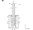
図1、図2、図3を用いて、第1実施形態の半導体装置101に関して説明する。半導体装置101は、第1半導体素子11、第2半導体素子12、正極金属板30、正極端子31、負極金属板40、負極端子41、出力金属板70、出力端子71などを備えている。半導体装置101は、2in1パッケージ構造をなしていると言える。半導体装置101は、例えば、インバータやコンバータなどの電力変換装置に適用することができる。
(First Embodiment)
The
なお、本実施形態では、負極金属板40が第1金属板に相当し、正極金属板30が第2金属板に相当し、出力金属板70が第3金属板に相当する。また、本実施形態では、正極端子31が第1端子に相当し、負極端子41が第2端子に相当する。
In the present embodiment, the
また、半導体装置101は、これらの構成要素が封止樹脂部20で覆われている。詳述すると、封止樹脂部20は、電気絶縁性の部材によって構成されており、半導体素子11、12と、正極金属板30と、負極金属板40と、出力金属板70とを覆っている。つまり、封止樹脂部20は、これらの構成要素と接しながら、これらの構成要素を封止していると言える。
Further, in the
本実施形態では、一例として、第1半導体素子11を上アーム半導体素子とし、第2半導体素子12を下アーム半導体素子とする半導体装置101を採用している。また、本実施形態では、半導体素子11、12の一例として、IGBT(Insulated‐Gate Bipolar Transistor)とダイオードを一体化したRC-IGBTを採用している。半導体素子11、12は、両面に電極を有する素子である。また、第1半導体素子11、第2半導体素子12は、半導体スイッチング素子である。しかしながら、本開示は、半導体素子11、12としてMOSFETを採用でき、もしくはIGBTとダイオードを上下アームそれぞれで1素子ずつ配置した計4素子の構成を採用することもできる。
In this embodiment, as an example, a
第1半導体素子11と第2半導体素子12は、直列接続されている。第1半導体素子11は、コレクタ電極が正極端子31と電気的に接続されており、エミッタ電極が第2半導体素子12のコレクタ電極と電気的に接続されている。第2半導体素子12は、コレクタ電極が第1半導体素子11のエミッタ電極と電気的に接続されており、エミッタ電極が負極端子41と電気的に接続されている。
The
図1に示すように、第1半導体素子11と第2半導体素子12は、XY平面において矩形状をなしており、X方向に並んで配置されている。また、図2、図3に示すように、第1半導体素子11と第2半導体素子12は、Z方向に厚みを有している。このため、第1半導体素子11と第2半導体素子12は、直方体状をなしていると言える。半導体素子11、12は、一方の面にコレクタ電極が形成されており、他方の面(反対面)にエミッタ電極が形成されている。
As shown in FIG. 1, the
第1半導体素子11と第2半導体素子12は、互いのコレクタ電極が同じ方向を向くように配置されている。よって、第1半導体素子11と第2半導体素子12は、互いのエミッタ電極が同じ方向を向くように配置されている。つまり、第1半導体素子11と第2半導体素子12は、エミッタ電極が負極金属板40と対向するように配置されている。
The
図2、図3に示すように、第1半導体素子11は、負極金属板40と正極金属板30との間に配置されている。第1半導体素子11は、コレクタ電極が正極金属板30と対向配置されている。コレクタ電極は、導電性の接続部材を介して、正極金属板30と電気的及び機械的に接続されている。なお、本開示では、導電性の接続部材の一例として、はんだを採用する。しかしながら、導電性の接続部材は、はんだに限定されず、銀ペーストなどであっても採用できる。
As shown in FIGS. 2 and 3, the
第1半導体素子11は、エミッタ電極が第2絶縁配線基板60の第1金属体62と対向配置されている。エミッタ電極は、はんだを介して、第1金属体62と電気的及び機械的に接続されている。エミッタ電極は、はんだ、第1金属体62を介して、出力金属板70と電気的に接続されている。また、エミッタ電極は、第1金属体62、はんだ、出力金属板70を介して、第2半導体素子12のコレクタ電極と電気的に接続されている。さらに、第1半導体素子11のエミッタ電極は、第2絶縁配線基板60の第2絶縁基板61によって、負極金属板40と電気的に絶縁されている。第2絶縁基板61は、絶縁体に相当する。
In the
なお、第1半導体素子11のコレクタ電極は、正極金属板側の電極に相当する。第1半導体素子11のエミッタ電極は、負極金属板側の電極に相当する。また、第2絶縁配線基板60に関しては、後程詳しく説明する。
The collector electrode of the
一方、第2半導体素子12は、負極金属板40と出力金属板70との間に配置されている。第2半導体素子12は、コレクタ電極が出力金属板70と対向配置されている。コレクタ電極は、はんだを介して、出力金属板70と電気的及び機械的に接続されている。また、第2半導体素子12は、エミッタ電極が負極金属板40と対向配置されている。エミッタ電極は、はんだ及びターミナル80を介して、負極金属板40と電気的及び機械的に接続されている。なお、第2半導体素子12のコレクタ電極は、出力金属板側の電極に相当する。第2半導体素子12のエミッタ電極は、負極金属板側の電極に相当する。ターミナル80は、例えば銅やアルミニウムなどの金属によって構成されたブロック体である。
On the other hand, the
正極金属板30は、例えば銅やアルミニウムなどの金属によって構成されている。正極金属板30は、例えば直方体状のブロック体である。本実施形態では、半導体素子11、12よりもZ方向の厚さが十分に厚く、XY平面における面積が広い正極金属板30を採用している。よって、半導体装置101は、正極金属板30の対向領域内に第1半導体素子11がおさまるように配置することができる。また、正極金属板30は、Z方向において、負極金属板40と対向配置されている。さらに、正極金属板30は、負極金属板40との間に第1半導体素子11が配置された状態で、負極金属板40と対向配置されていると言える。
The positive
図2に示すように、正極金属板30は、はんだを介して、正極端子31と電気的及び機械的に接続されている。よって、正極金属板30は、正極端子31と同電位となる。また、正極金属板30は、電流経路の一部としての機能を有している。
As shown in FIG. 2, the positive
正極金属板30は、第1半導体素子11のコレクタ電極とはんだを介して接続されているため、第1半導体素子11と熱的に接続されているとも言える。よって、正極金属板30は、第1半導体素子11から発せられた熱がはんだを介して伝達される。そして、正極金属板30は、第1半導体素子11との対向面の反対面が封止樹脂部20から露出している。このため、正極金属板30は、第1半導体素子11から伝達された熱を、封止樹脂部20から露出した露出面から放熱することができる。このように、正極金属板30は、ヒートシンクとしての機能を有している。なお、露出面は、周囲の封止樹脂部20と面一、もしくは、周囲の封止樹脂部20よりも突出している。また、露出面は、放熱面とも言える。
Since the positive
出力金属板70は、正極金属板30と同じ材料で構成されており、正極金属板30と同様の厚みを有している。しかしながら、図1に示すように、出力金属板70は、出力端子71と一体物として構成されている。出力金属板70は、例えば直方体状のブロック体をなしている。出力端子71は、出力金属板70の一部から突出した部位である。よって、出力金属板70は、出力端子71と同電位となる。また、出力金属板70は、電流経路の一部としての機能を有している。なお、出力端子71と出力金属板70は、別体に構成された金属体が、はんだなどで接続されていてもよい。
The
本実実施形態では、XY平面における面積が正極金属板30よりも広い出力金属板70を採用している。詳述すると、出力金属板70は、正極金属板30とY方向の長さが同様であり、正極金属板30よりもX方向の長さが長い。よって、第2半導体素子12は、出力金属板70の対向領域内におさまるように設けられている。また、出力金属板70は、第2半導体素子12との対向面に、第1金属体62を接続するための領域を形成することができる。
In the present embodiment, the
出力金属板70は、正極金属板30と同様、Z方向において、負極金属板40と対向配置されている。出力金属板70は、負極金属板40との間に第2半導体素子12が配置された状態で、負極金属板40と対向配置されている。また、出力金属板70は、X方向において、正極金属板30と並んで配置されている。出力金属板70と正極金属板30は、封止樹脂部20を介して隣り合って配置されている。このため、出力金属板70と正極金属板30は、封止樹脂部20によって電気的に絶縁されている。
Like the positive
出力金属板70は、第2半導体素子12のコレクタ電極とはんだを介して接続しているため、第2半導体素子12と熱的に接続されていると言える。よって、出力金属板70は、第2半導体素子12から発せられた熱がはんだを介して伝達される。そして、出力金属板70は、第2半導体素子12との対向面の反対面が封止樹脂部20から露出している。このため、出力金属板70は、第2半導体素子12から伝達された熱を、封止樹脂部20から露出した露出面から放熱することができる。このように、出力金属板70は、ヒートシンクとしての機能を有している。なお、露出面は、周囲の封止樹脂部20と面一、もしくは、周囲の封止樹脂部20よりも突出している。
Since the
負極金属板40は、正極金属板30と同じ材料で構成されており、正極金属板30と同様の形状及び厚みを有している。しかしながら、負極金属板40は、XY平面における面積が正極金属板30や出力金属板70よりも広い。詳述すると、負極金属板40は、正極金属板30や出力金属板70とY方向の長さが同様であり、正極金属板30や出力金属板70よりもX方向の長さが長い。また、負極金属板40のX方向の長さは、正極金属板30のX方向の長さと、出力金属板70のX方向の長さとを加算した長さよりも長い。
The negative
よって、半導体装置101は、負極金属板40の対向領域内に、第1半導体素子11と第2半導体素子12の両方がおさまるように配置することができる。また、半導体装置101は、負極金属板40の対向領域内に、正極金属板30と出力金属板70の両方がおさまるように配置することができる。このように、負極金属板40は、第1半導体素子11と第2半導体素子12の両方に対向配置されている。
Therefore, the
図2に示すように、負極金属板40は、はんだを介して、負極端子41と電気的及び機械的に接続されている。よって、負極金属板40は、負極端子41と同電位となる。また、負極金属板40は、電流経路の一部としての機能を有している。
As shown in FIG. 2, the negative
負極金属板40は、第2半導体素子12のエミッタ電極とはんだを介して接続されているため、第2半導体素子12と熱的に接続されていると言える。また、負極金属板40は、第2絶縁配線基板60の第2金属体63とはんだを介して接続されている。第2絶縁配線基板60は、第1金属体62に、第1半導体素子11のエミッタ電極が接続されている。後程説明するが、第1金属体62と第2金属体63は、第2絶縁基板61の表裏面に形成された金属体である。第1半導体素子11で発せられた熱は、第2絶縁配線基板60を介して負極金属板40に伝達される。このため、負極金属板40は、第2絶縁基板61によって、第1半導体素子11のエミッタ電極と電気的に絶縁された状態で熱的に接続されていると言える。従って、負極金属板40は、第1半導体素子11から発せられた熱と、第2半導体素子12から発せられた熱が伝達される。
Since the negative
そして、負極金属板40は、第2半導体素子12との対向面の反対面が封止樹脂部20から露出している。このため、負極金属板40は、両半導体素子11、12から伝達された熱を、封止樹脂部20から露出した露出面から放熱することができる。このように、負極金属板40は、ヒートシンクとしての機能を有している。
The surface of the negative
正極端子31と負極端子41は、半導体装置101の外部に設けられた装置や回路と、半導体装置101とを電気的に接続するための端子である。つまり、極端子31と負極端子41は、外部接続用端子である。
The
極端子31と負極端子41は、対向配置されている。図1、図2に示すように、正極端子31は、第2半導体素子12よりも第1半導体素子11側に偏った位置に配置されている。正極端子31は、Y方向において、第1半導体素子11と隣り合って配置されているとも言える。言い換えると、正極端子31は、XY平面のY方向において、第1半導体素子11と並んで配置されている。負極端子41は、正極端子31との間で電流が流れる端子であり、正極端子31と対向配置されている。よって、負極端子41は、XY平面において、第1半導体素子11に対してY方向側に配置されている。
The
正極端子31と負極端子41は、互いに電気的に絶縁するために、電気絶縁性の部材である第1絶縁基板51を間に配置した状態で対向配置されている。また、本実施形態では、一例として、第1絶縁基板51の表裏面に形成された金属体で構成されたと正極端子31と負極端子41を採用している。つまり、正極端子31と負極端子41は、第1絶縁配線基板50における第1絶縁基板51の表裏面に形成された金属体である。第1絶縁基板51は、絶縁板に相当する。
In order to electrically insulate the
第1絶縁配線基板50は、窒化ケイ素などのセラミックスで構成された第1絶縁基板51の表裏面に、銅などの金属体で正極端子31と負極端子41が形成されて一体化された基板である。つまり、第1絶縁配線基板50は、第1絶縁基板51の一方の面に形成された金属体が正極端子31を含んでおり、第1絶縁基板51の他方の面に形成された金属体が負極端子41を含んでいる。正極端子31、負極端子41は、例えば、第1絶縁基板51上に形成された金属体をパターニングすることで形成される。
The first
第1絶縁配線基板50は、一端が正極電極板30と負極電極板40との対向領域に配置されており、その他の部位が対向領域外に配置されている。なお、第1絶縁配線基板50は、第1絶縁基板51としてセラミックスを採用しているため熱伝導率が良好である。
One end of the first
半導体装置101は、第1絶縁配線基板50を備えることで、正極端子31、第1絶縁基板51、負極端子41を一つの部品で構成することができる。また、半導体装置101は、第1絶縁基板51によって、正極端子31と負極端子41との間の電気絶縁性を確保しつつ、正極端子31と負極端子41とを対向配置(平行に配置)することができる。
The
なお、第1絶縁配線基板50は、一部が封止樹脂部20で覆われ、その他の部位が封止樹脂部20から露出している。第1絶縁配線基板50は、少なくとも正極端子31の一部と、少なくとも負極端子41の一部が封止樹脂部20から露出している。本開示は、極端子31と負極端子41が対向配置されていなくてもよい。また、本開示は、正極端子31が第2半導体素子12よりも第1半導体素子11側に偏った位置に配置されていなくてもよい。
The first
第2絶縁配線基板60は、窒化ケイ素などのセラミックスで構成された第2絶縁基板61の表裏面に、銅などの金属体で第1金属体62と第2金属体63が形成されて一体化された基板である。第2絶縁配線基板60は、第2絶縁基板61の一方の面に形成された金属体が第1金属体62を含んでおり、第2絶縁基板61の他方の面に形成された金属体が第2金属体63を含んでいる。第1金属体62と第2金属体63とは、第2絶縁基板61によって電気的に絶縁されている。第1金属体62と第2金属体63は、例えば、第2絶縁基板61上に形成された金属体をパターニングすることで形成される。
The second
第2絶縁配線基板60は、第1半導体素子11に対向する位置、及び出力金属板70の端部に対向する位置に配置されている。つまり、第2絶縁配線基板60は、第1半導体素子11の上方から、出力金属板70の端部の上方にわたって設けられている。また、第1金属体62は、第1半導体素子11に対向する位置、及び出力金属板70の端部に対向する位置に配置されている。そして、第1金属体62には、第1半導体素子11のエミッタ電極と、出力金属板70が電気的に接続されている。一方、第2金属体63は、負極電極板40と電気的に接続されている。
The second
第2絶縁配線基板60は、上記のように、第2絶縁基板61としてセラミックスを採用しているため熱伝導率が良好である。よって、第1半導体素子11から発せられた熱は、はんだ、第2絶縁配線基板60を介して負極電極板40に伝達されやすい。このため、第1半導体素子11のエミッタ電極は、第2絶縁基板61によって、負極金属板40と電気的に絶縁された状態で、負極金属板40と熱的に接続されていると言える。しかしながら、第1半導体素子11で発せられた熱は、第2絶縁基板61としてセラミックスを採用していなくても、負極金属板40に伝達される。
As described above, the second
第1金属体62は、第1半導体素子11におけるエミッタ電極と出力金属板70とを電気的に接続する接続部に相当する。第1金属体62は、図3に示すように、エミッタ電極と対向する対向部、及び出力金属板70と対向する対向部との間が、両対向部よりも窪んだ凹部62aを含んでいる。つまり、凹部62aは、第1金属体62における、Z方向の厚みが周辺よりも薄い部位である。凹部62aは、少なくとも第1半導体素子11の端部におけるY方向の全域に対向する位置に設けられている。これによって、第1金属体62は、第1半導体素子11のコレクタ電極や正極金属板30との絶縁距離を確保しやすくなる。
The
ここで、図2、図3を用いて、半導体装置101の動作に関して説明する。図2、図3における破線矢印は、正極端子から負極端子の間の概略的な電流の流れ(電流経路)を示している。なお、電流の向きはインバータ動作状態によるため、正極から負極の向きとは限らない。
Here, the operation of the
半導体装置101は、正極端子31から負極端子41へと電流が流れる。詳述すると、半導体装置101は、正極端子31、正極金属板30、第1半導体素子11、第1金属体62、出力金属板70、第2半導体素子12、ターミナル80、負極金属板40、負極端子41の順で電流が流れる電流経路が形成されている。なお、半導体装置101は、N字タイプの接続構造を有していると言える。また、半導体装置101は、各構成要素間を電気的に接続しているはんだにも電流が流れる。しかしながら、ここでは、説明を簡略化するために、省略している。
In the
そして、半導体装置101は、図2に示すように、正極端子31から正極金属板30への電流経路が、負極金属板40から負極端子41への電流経路と対向配置され、電流の向きが逆向きとなっている。また、半導体装置101は、図3に示すように、正極金属板30から出力金属板70への電流経路が、負極金属板40の電流経路と対向配置され、電流の向きが逆向きとなっている。詳述すると、半導体装置101は、正極金属板30から第1金属体62を介する出力金属板70への電流経路が、負極金属板40から第2金属体63への電流経路と対向配置され、電流の向きが逆向きとなっている。
Then, as shown in FIG. 2, in the
よって、本開示は、正極端子31から負極端子41までの電流経路において、電流経路が対向配置され、電流の向きが逆向きとなる区間を増やすことができ配線のインダクタンスを低減できる。さらに、本開示は、中間電極を用いることなくインダクタンスを低減できるため、体格が大きくなることを抑制できる。また、半導体装置101は、電流ループを小さくすることができ電気的特性を優れたものとすることができるとも言える。
Therefore, in the present disclosure, in the current path from the
以上、本開示の好ましい実施形態について説明した。しかしながら、本開示は、上記実施形態に何ら制限されることはなく、本開示の趣旨を逸脱しない範囲において、種々の変形が可能である。以下に、本開示のその他の形態として、第2~第5実施形態、変形例1~7に関して説明する。上記実施形態及び第2~第5実施形態、変形例1~7は、夫々単独で実施することも可能であるが、適宜組み合わせて実施することも可能である。本開示は、実施形態において示された組み合わせに限定されることなく、種々の組み合わせによって実施可能である。 The preferred embodiments of the present disclosure have been described above. However, the present disclosure is not limited to the above-described embodiment, and various modifications can be made without departing from the spirit of the present disclosure. Hereinafter, as other embodiments of the present disclosure, the second to fifth embodiments and the modified examples 1 to 7 will be described. The above-described embodiment, the second to fifth embodiments, and the modified examples 1 to 7 can be carried out individually, but can also be carried out in combination as appropriate. The present disclosure is not limited to the combinations shown in the embodiments, but can be carried out by various combinations.
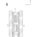
(第2実施形態)
図4を用いて、第2実施形態の半導体装置102に関して説明する。半導体装置102は、主に、第1絶縁配線基板50を用いない点が半導体装置101と異なる。半導体装置102は、半導体装置101と同様に、N字タイプの接続構造を有している。なお、図4は、図2に相当する断面図である。
(Second Embodiment)
The
半導体装置102は、正極金属板302と正極端子312とが一体的に構成された金属部材と、負極金属板402と負極端子412とが一体的に構成された金属部材とを備えている。正極端子312と負極端子412は、対向配置されており、封止樹脂部202で電気的に絶縁されている。
The
半導体装置102は、半導体装置101と同様の効果を奏することができる。さらに、半導体装置102は、正極端子312と負極端子412とを封止樹脂部202で電気的に絶縁している。このため、半導体装置102は、半導体装置101よりも、正極端子312と負極端子412との絶縁距離を長くすることができる。また、半導体装置102は、第1絶縁配線基板50が不要になり、半導体装置101よりも低コスト化できるメリットもある。
The
(第3実施形態)
図5を用いて、第3実施形態の半導体装置103に関して説明する。半導体装置103は、主に、絶縁配線基板503を用いる点が半導体装置101と異なる。半導体装置103は、半導体装置101と同様に、N字タイプの接続構造を有している。なお、図5は、図2に相当する断面図である。
(Third Embodiment)
The
絶縁配線基板503は、絶縁基板513の一方の面に形成された金属体が第1金属体62と正極端子313を含んでおり、絶縁基板513の他方の面に形成された金属体が負極端子413を含んでいる。負極端子413は、第1実施形態の第2金属体63と負極端子41とが一体化されたものとみなすことができる。絶縁配線基板503は、第1絶縁配線基板50や第2絶縁配線基板60と同様の材料によって構成することができ、同様の方法によって製造することができる。このように、絶縁配線基板503は、第1絶縁配線基板50と第2絶縁配線基板60とが一体的に形成されたものに相当する。なお、絶縁基板513は、絶縁体に相当する。
In the insulating
半導体装置103は、半導体装置101と同様の効果を奏することができる。さらに、半導体装置103は、絶縁配線基板503を有しているため、絶縁基板513と、第1金属体62と、正極端子313と、負極端子413とを一体物とすることができる。また、半導体装置103は、第1絶縁配線基板50と第2絶縁配線基板60の二つの絶縁配線基板を用いる必要がない。
The
(第4実施形態)
図6~図9を用いて、第4実施形態の半導体装置104に関して説明する。半導体装置104は、主に、絶縁配線基板504を用いる点が半導体装置101と異なる。半導体装置104は、半導体装置101と同様に、N字タイプの接続構造を有している。なお、本実施形態では、図面が煩雑になることを抑制するために、封止樹脂部20の図示を省略している。
(Fourth Embodiment)
The
図6に示すように、半導体装置104は、絶縁配線基板504、第1信号端子S1、第2信号端子S2を備えている。絶縁配線基板504は、絶縁基板514の一方の面に形成された金属体と、絶縁基板514の他方の面に形成された金属体とを含んでいる。絶縁配線基板504は、第1絶縁配線基板50や第2絶縁配線基板60と同様の材料によって構成することができ、同様の方法によって製造することができる。
As shown in FIG. 6, the
図6、図7、図8、図9に示すように、絶縁基板514の一方の面に形成された金属体は、第1金属体62と正極端子に加えて、信号用金属体524を含んでいる。なお、半導体装置104の正極端子は、半導体装置103の正極端子313と同様の構成を有している。
As shown in FIGS. 6, 7, 8 and 9, the metal body formed on one surface of the insulating
絶縁基板514は、複数の信号用金属体524が設けられている。図7に示すように、信号用金属体524は、例えば、半導体素子11、12のゲート電極に電気的に接続され、且つ、信号用端子S2(S1)に電気的に接続されている。
The insulating
なお、半導体装置104は、半導体素子11、12の温度を検出するための感温ダイオードなどを備えていてもよい。この場合、信号用端子S1、S2は、感温ダイオードと電気的に接続されたものを含んでいてもよい。
The
詳述すると、絶縁基板514は、Y方向に沿う複数の信号用金属体524が、X方向に並んで設けられている。また、絶縁基板514は、第1半導体素子11を基準として、正極端子とは反対側に、複数の信号用金属体524が設けられている。さらに、絶縁基板514は、第2半導体素子12を基準として、出力端子71とは反対側に、複数の信号用金属体524が設けられている。つまり、絶縁基板514の一方の面は、Y方向において、信号用金属体524、第1金属体62、正極端子がこの順番で並んで配置され、且つ、信号用金属体524、接続用金属体534がこの順番で並んで配置されている。
More specifically, the insulating
一方、絶縁基板514の他方の面に形成された金属体は、図8、図9に示すように、負極端子414を含んでいる。負極端子414は、負極端子413と同様、正極端子と対向配置されている。負極端子414と正極端子は、絶縁基板514によって電気的に絶縁されている。負極端子414としての金属体は、封止樹脂部20から突出する位置に加えて、第1半導体素子11の対向領域から第2半導体素子12の対向領域にわたって設けられており、一体的に設けられている。
On the other hand, the metal body formed on the other surface of the insulating
さらに、図9に示すように、負極端子414は、接続用金属体534と一体的に設けられている。絶縁基板514は、第2半導体素子12に対向する位置に貫通穴514aが形成されている。接続用金属体534は、貫通穴514aに設けられており、且つ、絶縁基板514の一方の面側と他方の面側とにわたって設けられている。
Further, as shown in FIG. 9, the
負極端子414及び接続用金属体534は、はんだを介して、負極金属板40と電気的及び機械的に接続されている。また、接続用金属体534は、はんだを介して、第2半導体素子12のエミッタ電極と電気的及び機械的に接続されている。これによって、第2半導体素子12のエミッタ電極は、負極端子414と電気的に接続されている。
The
半導体装置104は、半導体装置101と同様の効果を奏することができる。また、半導体装置104は、XY平面において、左右均等に絶縁配線基板504を配置できるため、応力バランスがとりやすい。つまり、半導体装置104は、構成要素間の線膨張係数差による応力が局所的に発生することを抑制できる。詳述すると、半導体装置104は、半導体素子11、12や、各接続部に応力が発生することを抑制できる。よって、半導体装置104は、応力が局所的に発生する場合よりも、電気的な信頼性を向上できる。
The
さらに、半導体装置104は、絶縁配線基板504が第1金属体62及び接続用金属体534に加えて、信号用金属体524を有している。このため、半導体装置104は、絶縁配線基板504と半導体素子11、12との接続と同時に、絶縁配線基板504と第1信号端子S1及び第2信号端子S2の接続を行うことができる。
Further, in the
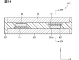
(第5実施形態)
図10~図12を用いて、第5実施形態の半導体装置105に関して説明する。半導体装置105は、主に、半導体素子11、12の配置が半導体装置101と異なる。半導体装置105は、半導体装置101と異なり、U字タイプの接続構造を有している。なお、本実施形態では、図面が煩雑になることを抑制するために、封止樹脂部20の図示を省略している。
(Fifth Embodiment)
The
半導体装置105は、上アーム半導体素子としての第1半導体素子11と、第1半導体素子と直列接続された下アーム半導体素子としての第2半導体素子12とを備えている。半導体装置105は、第1半導体素子11と第2半導体素子12が逆向きに配置されている。
The
つまり、半導体素子11、12は、第1半導体素子11のエミッタ電極と、第2半導体素子12のコレクタ電極が同じ方向を向くように配置されている。よって、半導体素子11、12は、第1半導体素子11のコレクタ電極と、第2半導体素子12のエミッタ電極が同じ方向を向くように配置されている。
That is, the
このため、図12に示すように、半導体装置105は、第1半導体素子11のエミッタ電極と第2半導体素子12のコレクタ電極が出力金属板70と対向配置されている。また、半導体装置105は、第1半導体素子11のコレクタ電極と第2半導体素子12のエミッタ電極が正極金属板30と対向配置されている。
Therefore, as shown in FIG. 12, in the
図11に示すように、半導体装置105は、絶縁配線基板505を備えている。絶縁配線基板505は、第1絶縁配線基板50などと同様に、窒化ケイ素などのセラミックスで構成された絶縁基板515の表裏面に、銅などの金属体が形成されて一体化された基板である。絶縁配線基板505は、第2半導体素子12の対向領域から、封止樹脂部20の外部にわたって設けられている。これによって、絶縁配線基板505は、後程説明する正極端子315と負極端子415を外部接続用端子とすることができる。
As shown in FIG. 11, the
絶縁配線基板505は、絶縁基板515の一方の面に形成された金属体が正極端子315を含んでおり、絶縁基板515の他方の面に形成された金属体が負極端子415を含んでいる。このように、半導体装置105は、半導体装置103と同様、絶縁配線基板505に正極端子315と負極端子415が形成されている。よって、正極端子315と負極端子415は、絶縁基板515を介して対向配置されており、絶縁基板515によって電気的に絶縁されている。
In the
また、図10に示すように、絶縁配線基板505は、第1半導体素子よりも前記第2半導体素子側に偏った位置に配置されている。このため、正極端子315と負極端子415は、第1半導体素子11よりも第2半導体素子12側に偏った位置に配置されている。つまり、正極端子315と負極端子415は、XY平面のY方向において、第2半導体素子12と並んで配置されている。
Further, as shown in FIG. 10, the
図11、図12に示すように、半導体装置105は、正極金属板30と出力金属板70とが対向配置されている。正極金属板30と出力金属板70は、第1実施形態と同様の材料、同様の形状である。しかしながら、本実施形態では、第1実施形態と異なり、正極金属板30と出力金属板70とが同じ体格を有している。正極金属板30は、第1金属板に相当する。出力金属板70は、第2金属板に相当する。
As shown in FIGS. 11 and 12, in the
正極金属板30は、第1半導体素子11と第2半導体素子12の両方に対向配置され、正極端子315と電気的に接続されている。正極金属板30は、はんだを介して、正極端子315と電気的及び機械的に接続されている。なお、本開示は、正極端子315と負極端子415が、第1半導体素子11よりも第2半導体素子12側に偏った位置に配置されていなくてもよい。また、本開示は、正極端子315と負極端子415が対向配置されていなくてもよい。
The positive
出力金属板70は、正極金属板30との間に第1半導体素子11と第2半導体素子12が配置された状態で、第1半導体素子11と第2半導体素子12の両方に対向配置されている。なお、出力金属板70は、図10に示すように、出力端子71が設けられている。
The
封止樹脂部20は、第1実施形態と同様、第1半導体素子11、第2半導体素子12、正極金属板30、出力金属板70を覆う。そして、正極金属板30と出力金属板70は、第1半導体素子11及び第2半導体素子12と対向する面の反対面が封止樹脂部20から露出する。
The sealing
第1半導体素子11は、出力金属板70側の電極であるエミッタ電極が出力金属板70と電気的に接続されている。詳述すると、第1半導体素子11のエミッタ電極は、はんだを介してターミナル80と電気的及び機械的に接続されている。そして、ターミナル80は、はんだを介して、出力金属板70と電気的及び機械的に接続されている。
In the
また、第1半導体素子11は、正極金属板30側の電極であるコレクタ電極が、はんだを介して正極金属板30と電気的に接続されている。正極金属板30は、上記のように、正極端子315と電気的に接続されている。よって、第1半導体素子11のコレクタ電極は、正極金属板30を介して正極金属板30と電気的に接続されている。
Further, in the
第2半導体素子12は、出力金属板70側の電極であるコレクタ電極が、はんだを介して出力金属板70と電気的に接続されている。また、第2半導体素子12は、正極金属板30側の電極であるエミッタ電極が、はんだを介して負極端子415と電気的に接続されている。上記のように、負極端子415は、絶縁基板515によって正極端子315及び正極金属板30と電気的に絶縁されている。このため、第2半導体素子12のエミッタ電極は、絶縁基板515によって正極金属板30と電気的に絶縁された状態で熱的に接続されている。
In the
ここで、図10~図12を用いて、半導体装置105の動作に関して説明する。図10~図12における破線矢印は、概略的な電流の流れ(電流経路)を示している。
Here, the operation of the
半導体装置105は、正極端子315から負極端子415へと電流が流れる。詳述すると、半導体装置105は、正極端子315、正極金属板30、第1半導体素子11、ターミナル80、出力金属板70、第2半導体素子12、負極端子415の順で電流が流れる電流経路が形成されている。
In the
そして、正極端子315の電流経路は、負極端子415の電流経路と対向して逆向きの電流が流れる。また、正極金属板30の電流経路は、出力金属板70の電流経路と対向して逆向きの電流が流れる。このため、半導体装置105は、半導体装置101と同様の効果を奏することができる。
Then, the current path of the
ところで、例えば半導体装置101は、半導体素子11、12に対向する一方側に、正極金属板30と出力金属板70の二つの金属板が配置されている。このため、半導体装置101は、正極金属板30と出力金属板70との絶縁を確保する必要がある。そこで、半導体装置101は、正極金属板30と出力金属板70とを離して配置している。つまり、半導体装置101は、正極金属板30と出力金属板70とを絶縁するための絶縁スペースが必要である。
By the way, for example, in the
これに対して、半導体装置105は、各半導体素子11、12に対向する一方側に、正極金属板30が配置され、他方側に出力金属板70が配置されている。このように、半導体装置105は、X方向に金属板が配置されていないため、X方向に並ぶ金属板同士の絶縁を確保する必要がない。
On the other hand, in the
よって、半導体装置105は、絶縁スペースが必要ない分、半導体装置101よりも体格を小型化できる。なお、図10の二点鎖線は、X方向における、半導体装置101と半導体装置105との体格差を示している。
Therefore, the
(変形例1)
図13を用いて、変形例1における半導体装置106に関して説明する。半導体装置106は、主に、第1半導体素子11のエミッタ電極と負極金属板40とを絶縁する部材が半導体装置101と異なる。図13は、図3に相当する断面図である。
(Modification 1)
The
半導体装置106は、正極金属板30などと同様の材料によって構成された接続部材606を備えている。接続部材606は、第1半導体素子11のエミッタ電極と、出力金属板70とを電気的に接続する部材である。つまり、半導体装置106は、第1金属体62のかわりに、接続部材606を備えている。
The
封止樹脂部206は、封止樹脂部20と同様に、半導体素子11、12などを覆っている。しかしながら、封止樹脂部206は、接続部材606と負極金属板40との間に形成された介在部206aを含んでいる。接続部材606と負極金属板40は、介在部206aによって電気的に絶縁されている。つまり、第1半導体素子11のエミッタ電極は、介在部206aによって、負極金属板40と電気的に絶縁されている。
The sealing
介在部206aの厚みは、接続部材606と負極金属板40とを電気的に絶縁でき、且つ、第1半導体素子11で発せられた熱が負極金属板40に伝達される程度であればよい。また、介在部206aの厚みは、接続部材606と負極金属板40とを電気的に絶縁できる範囲で、できるだけ薄い方が、第1半導体素子11で発せられた熱が負極金属板40に伝達されやすいので好ましい。なお、介在部206aは、絶縁体に相当する。
The thickness of the intervening
半導体装置106は、半導体装置101と同様の効果を奏することができる。さらに、半導体装置106は、絶縁配線基板を備えることなく、封止樹脂部206によって電気絶縁性を確保することができる。
The
(変形例2)
図14、図15を用いて、変形例2における半導体装置107に関して説明する。半導体装置107は、主に、第2半導体素子12のエミッタ電極と正極金属板307とを絶縁する部材が半導体装置105と異なる。図14は、図12に相当する断面図である。図15は、図11に相当する断面図である。
(Modification 2)
The
図15に示すように、半導体装置107は、正極金属板307と正極端子317とが一体的に構成された金属部材と、負極金属板407と負極端子417とが一体的に構成された金属部材とを備えている。これらの金属部材は、正極金属板30などと同様の材料によって構成されている。
As shown in FIG. 15, the
負極金属板407は、第2半導体素子12のエミッタ電極と対向配置されており、第2半導体素子12のエミッタ電極とはんだを介して電気的に接続されている。また、負極金属板407は、第2半導体素子12のエミッタ電極と対向している面の反対面が、正極金属板307と対向している。
The negative
図14、図15に示すように、封止樹脂部207は、封止樹脂部20と同様に、半導体素子11、12などを覆っている。しかしながら、封止樹脂部207は、正極金属板307と負極金属板407との間に形成された介在部207aを含んでいる。正極金属板307と負極金属板407は、介在部207aによって電気的に絶縁されている。つまり、第2半導体素子12は、エミッタ電極が負極金属板407と電気的に接続され、且つ、介在部207aによって正極金属板307と電気的に絶縁されている。
As shown in FIGS. 14 and 15, the sealing
介在部207aの厚みは、正極金属板307と負極金属板407とを電気的に絶縁でき、且つ、第2半導体素子12で発せられた熱が正極金属板307に伝達される程度であればよい。また、介在部207aの厚みは、正極金属板307と負極金属板407とを電気的に絶縁できる範囲で、できるだけ薄い方が、第2半導体素子12で発せられた熱が正極金属板307に伝達されやすいので好ましい。なお、介在部207aは、絶縁体に相当する。
The thickness of the intervening
半導体装置107は、半導体装置101と同様の効果を奏することができる。さらに、半導体装置107は、絶縁配線基板を備えることなく、封止樹脂部207によって電気絶縁性を確保することができる。
The
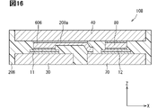
(変形例3)
図16を用いて、変形例3における半導体装置108に関して説明する。半導体装置108は、第1半導体素子11のエミッタ電極と負極金属板40とを絶縁する部材が半導体装置106と異なる。図16は、図3に相当する断面図である。
(Modification 3)
The
半導体装置108は、絶縁性接着剤208aによって、接続部材606と負極金属板40とが機械的に接続されている。このように、接続部材606と負極金属板40は、絶縁性接着剤208aによって電気的に絶縁されている。つまり、第1半導体素子11のエミッタ電極は、絶縁性接着剤208aによって、負極金属板40と電気的に絶縁されている。絶縁性接着剤208aは、絶縁体に相当する。
In the
絶縁性接着剤208aは、熱伝導率が高い程、第1半導体素子11のエミッタ電極と負極金属板40とを熱的に接続しやすくなるので好ましい。つまり、絶縁性接着剤208aは、熱伝導率が高い程、第1半導体素子11で発せられた熱が負極金属板40に伝達されやすいので好ましい。
The insulating
半導体装置108は、半導体装置106と同様の効果を奏することができる。さらに、半導体装置108は、封止樹脂部206と別部材の絶縁性接着剤208aで接続部材606と負極金属板40とを電気的に絶縁している。このため、半導体装置108は、半導体装置106よりも、第1半導体素子11のエミッタ電極と負極金属板40との間の熱の伝わりやすさを調整しやすい。
The
(変形例4)
図17を用いて、変形例4における半導体装置109に関して説明する。半導体装置109は、正極金属板307と負極金属板407とを絶縁する部材が半導体装置107と異なる。図17は、図14に相当する断面図である。
(Modification example 4)
The
半導体装置109は、絶縁性接着剤209aによって、正極金属板307と負極金属板407とが機械的に接続されている。このように、正極金属板307と負極金属板407は、絶縁性接着剤209aによって電気的に絶縁されている。つまり、第2半導体素子12のエミッタ電極は、絶縁性接着剤209aによって、正極金属板307と電気的に絶縁されている。絶縁性接着剤209aは、絶縁性接着剤208aであり、絶縁体に相当する。
In the
半導体装置109は、半導体装置107と同様の効果を奏することができる。さらに、半導体装置109は、封止樹脂部209と別部材の絶縁性接着剤209aで正極金属板307と負極金属板407とを電気的に絶縁している。このため、半導体装置109は、半導体装置107よりも、第2半導体素子12のエミッタ電極と正極金属板307との間の熱の伝わりやすさを調整しやすい。
The
ここまでに説明した半導体装置は、冷却器1010、1020に取り付けられてもよい。そこで、図18、図19、図20を用いて、半導体装置が冷却器1010と1020に取り付けられた構成の一例として、変形例5、6、7に関して説明する。半導体装置が冷却器1010と1020に取り付けられた構造体は、半導体モジュールとも言える。なお、冷却器1010、1020は、例えば、特開2018-101666号公報に記載されたものなどを採用することができる。
The semiconductor device described so far may be attached to the
変形例5は、図18に示すように、半導体装置101が第1冷却器1010と第2冷却器1020に取り付けられた構成をなしている。図18は、図3に相当する断面図である。
As shown in FIG. 18, the modification 5 has a configuration in which the
第1冷却器1010と第2冷却器1020は、銅やアルミニウムなどの金属によって構成されており、冷却水などの冷媒が流れる流路が形成されている。半導体装置101は、第1冷却器1010と第2冷却器1020とで挟み込まれている。
The
半導体装置101は、負極金属板40側に、第1絶縁体1030、第1外面金属体1040、第1冷却器1010がこの順番で積層配置されている。半導体モジュールは、負極金属板40と第1絶縁体1030が接しており、第1絶縁体1030と第1外面金属体1040とが接しており、第1外面金属体1040と第1冷却器1010とが接している。半導体装置101は、第1絶縁体1030によって、負極金属板40と第1冷却器1010が電気的に絶縁されている。なお、負極金属板40、第1絶縁体1030、第1外面金属体1040は、絶縁配線基板によって形成されていてもよい。
In the
半導体装置101は、負極金属板40側に、第1絶縁体1030、第1外面金属体1040、第1冷却器1010がこの順番で積層配置されている。よって、半導体装置101は、第1絶縁体1030によって、負極金属板40と第1冷却器1010が電気的に絶縁されている。なお、負極金属板40、第1絶縁体1030、第1外面金属体1040は、絶縁配線基板によって形成されていてもよい。
In the
また、半導体装置101は、正極金属板30及び出力金属板70側に、第2絶縁体1050、第2外面金属体1060、第2冷却器1020がこの順番で積層配置されている。半導体モジュールは、正極金属板30及び出力金属板70と第2絶縁体1050が接しており、第2絶縁体1050と第2外面金属体1060とが接しており、第2外面金属体1060と第2冷却器1020とが接している。半導体装置101は、第2絶縁体1050によって、正極金属板30及び出力金属板70と第2冷却器1020が電気的に絶縁されている。なお、正極金属板30、出力金属板70、第2絶縁体1050、第2外面金属体1060は、絶縁配線基板によって形成されていてもよい。
Further, in the
これによって、半導体装置101は、冷却器1010、1020と電気的に絶縁しつつ、冷却器1010、1020によって冷却することができる。
Thereby, the
変形例6は、図19に示すように、半導体装置104が第1冷却器1010と第2冷却器1020に取り付けられた構成をなしている。図19は、図8、図9に相当する断面図である。変形例6の半導体モジュールは、半導体装置104が変形例5の半導体モジュールと異なる。よって、変形例6の半導体モジュールは、変形例5と同様の効果を奏することができる。
As shown in FIG. 19, the modification 6 has a configuration in which the
変形例7は、図20に示すように、半導体装置105が第1冷却器1010と第2冷却器1020に取り付けられた構成をなしている。図20は、図12に相当する断面図である。変形例7の半導体モジュールは、半導体装置105が変形例5の半導体モジュールと異なる。よって、変形例7の半導体モジュールは、変形例5と同様の効果を奏することができる。
As shown in FIG. 20, the modification 7 has a configuration in which the
11…第1半導体素子、12…第2半導体素子、20…封止樹脂部、31…正極端子、30…正極金属板、41…負極端子、40…負極金属板、50…第1絶縁配線基板、51…第1絶縁基板、60…第2絶縁配線基板、61…第2絶縁基板、62…第1金属体、62a…凹部、63…第2金属体、71…出力端子、70…出力金属板、80…ターミナル、101~109…半導体装置 11 ... 1st semiconductor element, 12 ... 2nd semiconductor element, 20 ... Sealing resin part, 31 ... Positive terminal, 30 ... Positive metal plate, 41 ... Negative terminal, 40 ... Negative metal plate, 50 ... 1st insulated wiring substrate , 51 ... 1st insulated substrate, 60 ... 2nd insulated wiring substrate, 61 ... 2nd insulated substrate, 62 ... 1st metal body, 62a ... recess, 63 ... 2nd metal body, 71 ... output terminal, 70 ... output metal Plate, 80 ... Terminal, 101-109 ... Semiconductor device
Claims (15)
前記第1半導体素子と直列接続された第2半導体素子(12)と、
第1端子(31、312、313)と、
前記第1端子との間で電流が流れる第2端子(41、412、413、414)と、
前記第1半導体素子と前記第2半導体素子の両方に対向配置され、前記第2端子と電気的に接続された第1金属板(40、402)と、
前記第1金属板との間に前記第1半導体素子が配置された状態で、前記第1金属板と対向配置され、前記第1端子と電気的に接続された第2金属板(30、302)と、
前記第1金属板との間に前記第2半導体素子が配置された状態で、前記第1金属板と対向配置された第3金属板(70)と、を備え、
前記第2半導体素子は、前記第3金属板側の電極が前記第3金属板と電気的に接続され、前記第1金属板側の電極が前記第1金属板と電気的に接続され、
前記第1半導体素子は、前記第2金属板側の電極が前記第2金属板と電気的に接続され、前記第1金属板側の電極が前記第3金属板と電気的に接続されるとともに、絶縁体(61、513、514、206a、208a)によって前記第1金属板と電気的に絶縁された状態で熱的に接続され、
前記第1半導体素子、前記第2半導体素子、前記第1金属板、前記第2金属板、前記第3金属板を覆う封止樹脂部(20、202、206、208)を備えており、
前記第1金属板は、前記第1半導体素子及び前記第2半導体素子と対向する面の反対面が前記封止樹脂部から露出し、
前記第2金属板は、前記第1半導体素子と対向する面の反対面が前記封止樹脂部から露出し、
前記第3金属板は、前記第2半導体素子と対向する面の反対面が前記封止樹脂部から露出している半導体装置。 The first semiconductor element (11) and
A second semiconductor element (12) connected in series with the first semiconductor element,
First terminal (31, 312, 313) and
The second terminal (41, 412, 413, 414) through which a current flows between the first terminal and the terminal
A first metal plate (40, 402) arranged to face both the first semiconductor element and the second semiconductor element and electrically connected to the second terminal .
A second metal plate (30, 302) arranged facing the first metal plate and electrically connected to the first terminal in a state where the first semiconductor element is arranged between the first metal plate and the first metal plate. )When,
A third metal plate (70) arranged to face the first metal plate in a state where the second semiconductor element is arranged between the first metal plate and the first metal plate is provided.
In the second semiconductor element, the electrode on the third metal plate side is electrically connected to the third metal plate, and the electrode on the first metal plate side is electrically connected to the first metal plate.
In the first semiconductor element, the electrode on the second metal plate side is electrically connected to the second metal plate, and the electrode on the first metal plate side is electrically connected to the third metal plate. , Thermally connected to the first metal plate by an insulator (61, 513, 514, 206a, 208a) in a state of being electrically insulated.
A sealing resin portion (20, 202, 206, 208) that covers the first semiconductor element, the second semiconductor element, the first metal plate, the second metal plate, and the third metal plate is provided.
In the first metal plate, the opposite surface of the surface facing the first semiconductor element and the second semiconductor element is exposed from the sealing resin portion.
In the second metal plate, the opposite surface of the surface facing the first semiconductor element is exposed from the sealing resin portion.
The third metal plate is a semiconductor device in which the opposite surface of the surface facing the second semiconductor element is exposed from the sealing resin portion.
前記第2端子は、前記第1端子と対向配置されている請求項1に記載の半導体装置。 The first terminal is arranged at a position biased toward the first semiconductor element with respect to the second semiconductor element.
The semiconductor device according to claim 1 , wherein the second terminal is arranged to face the first terminal.
前記第1半導体素子と直列接続された第2半導体素子(12)と、
第1端子(315、317)と、
前記第1端子との間で電流が流れる第2端子(415、417)と、
前記第1半導体素子と前記第2半導体素子の両方に対向配置され、前記第1端子と電気的に接続された第1金属板(30、307)と、
前記第1金属板との間に前記第1半導体素子と前記第2半導体素子が配置された状態で、前記第1半導体素子と前記第2半導体素子の両方に対向配置された第2金属板(70)と、を備え、
前記第1半導体素子は、前記第2金属板側の電極が前記第2金属板と電気的に接続され、前記第1金属板側の電極が前記第1金属板と電気的に接続されるとともに、前記第1金属板を介して前記第1端子と電気的に接続され、
前記第2半導体素子は、前記第2金属板側の電極が前記第2金属板と電気的に接続され、前記第1金属板側の電極が前記第2端子と電気的に接続され、且つ、絶縁体(515、207a、209a)によって前記第1金属板と電気的に絶縁された状態で熱的に接続された半導体装置。 The first semiconductor element (11) and
A second semiconductor element (12) connected in series with the first semiconductor element,
With the first terminal (315, 317),
A second terminal (415, 417) through which a current flows between the first terminal and the terminal
A first metal plate (30, 307) arranged to face both the first semiconductor element and the second semiconductor element and electrically connected to the first terminal.
A second metal plate (2nd metal plate) arranged to face both the first semiconductor element and the second semiconductor element in a state where the first semiconductor element and the second semiconductor element are arranged between the first metal plate and the first metal plate. 70) and
In the first semiconductor element, the electrode on the second metal plate side is electrically connected to the second metal plate, and the electrode on the first metal plate side is electrically connected to the first metal plate. , Electrically connected to the first terminal via the first metal plate,
In the second semiconductor element, the electrode on the second metal plate side is electrically connected to the second metal plate, the electrode on the first metal plate side is electrically connected to the second terminal, and A semiconductor device thermally connected to the first metal plate in a state of being electrically insulated by an insulator (515, 207a, 209a).
前記第1金属板と前記第2金属板は、前記第1半導体素子及び前記第2半導体素子と対向する面の反対面が前記封止樹脂部から露出している請求項3に記載の半導体装置。 A sealing resin portion (207, 209) that covers the first semiconductor element, the second semiconductor element, the first metal plate, and the second metal plate is provided.
The semiconductor device according to claim 3 , wherein the first metal plate and the second metal plate have the opposite surfaces of the first semiconductor element and the surface facing the second semiconductor element exposed from the sealing resin portion. ..
前記絶縁板の一方の面に形成された前記金属体は、前記第1端子を含んでおり、
前記絶縁板の他方の面に形成された前記金属体は、前記第2端子を含んでいる請求項1乃至5のいずれか1項に記載の半導体装置。 It is equipped with an insulated wiring board (50, 503, 504, 505) in which a metal body is formed on the front and back surfaces of the insulating plate.
The metal body formed on one surface of the insulating plate includes the first terminal.
The semiconductor device according to any one of claims 1 to 5 , wherein the metal body formed on the other surface of the insulating plate includes the second terminal.
前記絶縁板は、前記絶縁体を含んでいる請求項1乃至5のいずれか1項に記載の半導体装置。 It is equipped with an insulated wiring board (60, 503, 504, 505) in which a metal body is formed on the front and back surfaces of the insulating plate.
The semiconductor device according to any one of claims 1 to 5 , wherein the insulating plate includes the insulator.
前記絶縁板は、前記絶縁体を含んでおり、
前記絶縁板の一方の面に形成された前記金属体は、前記第1端子を含んでおり、
前記絶縁板の他方の面に形成された前記金属体は、前記第2端子を含んでいる請求項1乃至5のいずれか1項に記載の半導体装置。 It is equipped with an insulated wiring board (503, 504, 505) in which a metal body is formed on the front and back surfaces of the insulating plate.
The insulating plate contains the insulator, and the insulating plate contains the insulator.
The metal body formed on one surface of the insulating plate includes the first terminal.
The semiconductor device according to any one of claims 1 to 5 , wherein the metal body formed on the other surface of the insulating plate includes the second terminal.
前記第1半導体素子と直列接続された第2半導体素子(12)と、
第1端子(31、312、313)と、
前記第1端子との間で電流が流れる第2端子(41、412、413、414)と、
前記第1半導体素子と前記第2半導体素子の両方に対向配置され、前記第2端子と電気的に接続された第1金属板(40、402)と、
前記第1金属板との間に前記第1半導体素子が配置された状態で、前記第1金属板と対向配置され、前記第1端子と電気的に接続された第2金属板(30、302)と、
前記第1金属板との間に前記第2半導体素子が配置された状態で、前記第1金属板と対向配置された第3金属板(70)と、を備え、
前記第2半導体素子は、前記第3金属板側の電極が前記第3金属板と電気的に接続され、前記第1金属板側の電極が前記第1金属板と電気的に接続され、
前記第1半導体素子は、前記第2金属板側の電極が前記第2金属板と電気的に接続され、前記第1金属板側の電極が前記第3金属板と電気的に接続されるとともに、絶縁体(61、513、514、206a、208a)によって前記第1金属板と電気的に絶縁された状態で熱的に接続され、
絶縁板の表裏面に金属体が形成された絶縁配線基板(60、503、504、505)を備えており、
前記絶縁板は、前記絶縁体を含んでいる半導体装置。 The first semiconductor element (11) and
A second semiconductor element (12) connected in series with the first semiconductor element,
First terminal (31, 312, 313) and
The second terminal (41, 412, 413, 414) through which a current flows between the first terminal and the terminal
A first metal plate (40, 402) arranged to face both the first semiconductor element and the second semiconductor element and electrically connected to the second terminal .
A second metal plate (30, 302) arranged facing the first metal plate and electrically connected to the first terminal in a state where the first semiconductor element is arranged between the first metal plate and the first metal plate. )When,
A third metal plate (70) arranged to face the first metal plate in a state where the second semiconductor element is arranged between the first metal plate and the first metal plate is provided.
In the second semiconductor element, the electrode on the third metal plate side is electrically connected to the third metal plate, and the electrode on the first metal plate side is electrically connected to the first metal plate.
In the first semiconductor element, the electrode on the second metal plate side is electrically connected to the second metal plate, and the electrode on the first metal plate side is electrically connected to the third metal plate. , Thermally connected to the first metal plate by an insulator (61, 513, 514, 206a, 208a) in a state of being electrically insulated .
It is equipped with an insulated wiring board (60, 503, 504, 505) in which a metal body is formed on the front and back surfaces of the insulating plate.
The insulating plate is a semiconductor device containing the insulator.
前記第1半導体素子と直列接続された第2半導体素子(12)と、
第1端子(31、312、313)と、
前記第1端子との間で電流が流れる第2端子(41、412、413、414)と、
前記第1半導体素子と前記第2半導体素子の両方に対向配置され、前記第2端子と電気的に接続された第1金属板(40、402)と、
前記第1金属板との間に前記第1半導体素子が配置された状態で、前記第1金属板と対向配置され、前記第1端子と電気的に接続された第2金属板(30、302)と、
前記第1金属板との間に前記第2半導体素子が配置された状態で、前記第1金属板と対向配置された第3金属板(70)と、を備え、
前記第2半導体素子は、前記第3金属板側の電極が前記第3金属板と電気的に接続され、前記第1金属板側の電極が前記第1金属板と電気的に接続され、
前記第1半導体素子は、前記第2金属板側の電極が前記第2金属板と電気的に接続され、前記第1金属板側の電極が前記第3金属板と電気的に接続されるとともに、絶縁体(61、513、514、206a、208a)によって前記第1金属板と電気的に絶縁された状態で熱的に接続され、
絶縁板の表裏面に金属体が形成された絶縁配線基板(503、504、505)を備えており、
前記絶縁板は、前記絶縁体を含んでおり、
前記絶縁板の一方の面に形成された前記金属体は、前記第1端子を含んでおり、
前記絶縁板の他方の面に形成された前記金属体は、前記第2端子を含んでいる半導体装置。 The first semiconductor element (11) and
A second semiconductor element (12) connected in series with the first semiconductor element,
First terminal (31, 312, 313) and
The second terminal (41, 412, 413, 414) through which a current flows between the first terminal and the terminal
A first metal plate (40, 402) arranged to face both the first semiconductor element and the second semiconductor element and electrically connected to the second terminal .
A second metal plate (30, 302) arranged facing the first metal plate and electrically connected to the first terminal in a state where the first semiconductor element is arranged between the first metal plate and the first metal plate. )When,
A third metal plate (70) arranged to face the first metal plate in a state where the second semiconductor element is arranged between the first metal plate and the first metal plate is provided.
In the second semiconductor element, the electrode on the third metal plate side is electrically connected to the third metal plate, and the electrode on the first metal plate side is electrically connected to the first metal plate.
In the first semiconductor element, the electrode on the second metal plate side is electrically connected to the second metal plate, and the electrode on the first metal plate side is electrically connected to the third metal plate. , Thermally connected to the first metal plate by an insulator (61, 513, 514, 206a, 208a) in a state of being electrically insulated .
It is equipped with an insulated wiring board (503, 504, 505) in which a metal body is formed on the front and back surfaces of the insulating plate.
The insulating plate contains the insulator, and the insulating plate contains the insulator.
The metal body formed on one surface of the insulating plate includes the first terminal.
The metal body formed on the other surface of the insulating plate is a semiconductor device including the second terminal.
前記表裏面の前記金属体は、前記貫通穴を介して電気的に接続されている請求項7乃至10のいずれか1項に記載の半導体装置。 The insulated wiring board has a through hole formed in the insulating plate.
The semiconductor device according to any one of claims 7 to 10 , wherein the metal bodies on the front and back surfaces are electrically connected via the through holes.
前記金属体は、前記信号端子と電気的に接続された信号用金属体(524)を含んでいる請求項7乃至11のいずれか1項に記載の半導体装置。 Equipped with signal terminals (S1, S2),
The semiconductor device according to any one of claims 7 to 11 , wherein the metal body includes a metal body for signals (524) electrically connected to the signal terminal.
前記第1半導体素子と直列接続された第2半導体素子(12)と、
第1端子(31、312、313)と、
前記第1端子との間で電流が流れる第2端子(41、412、413、414)と、
前記第1半導体素子と前記第2半導体素子の両方に対向配置され、前記第2端子と電気的に接続された第1金属板(40、402)と、
前記第1金属板との間に前記第1半導体素子が配置された状態で、前記第1金属板と対向配置され、前記第1端子と電気的に接続された第2金属板(30、302)と、
前記第1金属板との間に前記第2半導体素子が配置された状態で、前記第1金属板と対向配置された第3金属板(70)と、を備え、
前記第2半導体素子は、前記第3金属板側の電極が前記第3金属板と電気的に接続され、前記第1金属板側の電極が前記第1金属板と電気的に接続され、
前記第1半導体素子は、前記第2金属板側の電極が前記第2金属板と電気的に接続され、前記第1金属板側の電極が前記第3金属板と電気的に接続されるとともに、絶縁体(61、513、514、206a、208a)によって前記第1金属板と電気的に絶縁された状態で熱的に接続され、
絶縁板の表裏面に金属体が形成された絶縁配線基板(50、503、504、505)を備えており、
前記絶縁板の一方の面に形成された前記金属体は、前記第1端子を含んでおり、
前記絶縁板の他方の面に形成された前記金属体は、前記第2端子を含んでいる半導体装置。 The first semiconductor element (11) and
A second semiconductor element (12) connected in series with the first semiconductor element,
First terminal (31, 312, 313) and
The second terminal (41, 412, 413, 414) through which a current flows between the first terminal and the terminal
A first metal plate (40, 402) arranged to face both the first semiconductor element and the second semiconductor element and electrically connected to the second terminal .
A second metal plate (30, 302) arranged facing the first metal plate and electrically connected to the first terminal in a state where the first semiconductor element is arranged between the first metal plate and the first metal plate. )When,
A third metal plate (70) arranged to face the first metal plate in a state where the second semiconductor element is arranged between the first metal plate and the first metal plate is provided.
In the second semiconductor element, the electrode on the third metal plate side is electrically connected to the third metal plate, and the electrode on the first metal plate side is electrically connected to the first metal plate.
In the first semiconductor element, the electrode on the second metal plate side is electrically connected to the second metal plate, and the electrode on the first metal plate side is electrically connected to the third metal plate. , Thermally connected to the first metal plate by an insulator (61, 513, 514, 206a, 208a) in a state of being electrically insulated .
It is equipped with an insulated wiring board (50, 503, 504, 505) in which a metal body is formed on the front and back surfaces of the insulating plate.
The metal body formed on one surface of the insulating plate includes the first terminal.
The metal body formed on the other surface of the insulating plate is a semiconductor device including the second terminal.
前記第1半導体素子と直列接続された第2半導体素子(12)と、
第1端子(31、312、313)と、
前記第1端子との間で電流が流れる第2端子(41、412、413、414)と、
前記第1半導体素子と前記第2半導体素子の両方に対向配置され、前記第2端子と電気的に接続された第1金属板(40、402)と、
前記第1金属板との間に前記第1半導体素子が配置された状態で、前記第1金属板と対向配置され、前記第1端子と電気的に接続された第2金属板(30、302)と、
前記第1金属板との間に前記第2半導体素子が配置された状態で、前記第1金属板と対向配置された第3金属板(70)と、を備え、
前記第2半導体素子は、前記第3金属板側の電極が前記第3金属板と電気的に接続され、前記第1金属板側の電極が前記第1金属板と電気的に接続され、
前記第1半導体素子は、前記第2金属板側の電極が前記第2金属板と電気的に接続され、前記第1金属板側の電極が前記第3金属板と電気的に接続されるとともに、絶縁体(61、513、514、206a、208a)によって前記第1金属板と電気的に絶縁された状態で熱的に接続され、
絶縁板の表裏面に金属体が形成された絶縁配線基板(60、504)を備えており、
前記絶縁板の一方の面に形成された前記金属体は、前記第1半導体素子における前記第1金属板側の電極と前記第3金属板とを電気的に接続する接続部(62、62a)を含んでおり、
前記接続部は、前記第1金属板側の電極と対向する対向部、及び前記第3金属板と対向する対向部との間が、両対向部よりも窪んだ凹部を含んでいる半導体装置。 The first semiconductor element (11) and
A second semiconductor element (12) connected in series with the first semiconductor element,
First terminal (31, 312, 313) and
The second terminal (41, 412, 413, 414) through which a current flows between the first terminal and the terminal
A first metal plate (40, 402) arranged to face both the first semiconductor element and the second semiconductor element and electrically connected to the second terminal .
A second metal plate (30, 302) arranged facing the first metal plate and electrically connected to the first terminal in a state where the first semiconductor element is arranged between the first metal plate and the first metal plate. )When,
A third metal plate (70) arranged to face the first metal plate in a state where the second semiconductor element is arranged between the first metal plate and the first metal plate is provided.
In the second semiconductor element, the electrode on the third metal plate side is electrically connected to the third metal plate, and the electrode on the first metal plate side is electrically connected to the first metal plate.
In the first semiconductor element, the electrode on the second metal plate side is electrically connected to the second metal plate, and the electrode on the first metal plate side is electrically connected to the third metal plate. , Thermally connected to the first metal plate by an insulator (61, 513, 514, 206a, 208a) in a state of being electrically insulated .
It is equipped with an insulated wiring board (60, 504) in which a metal body is formed on the front and back surfaces of the insulating plate.
The metal body formed on one surface of the insulating plate is a connecting portion (62, 62a) for electrically connecting the electrode on the first metal plate side and the third metal plate in the first semiconductor element. Includes
The connection portion is a semiconductor device including a recessed portion between the facing portion facing the electrode on the first metal plate side and the facing portion facing the third metal plate, which is recessed from both facing portions.
前記第1金属板は、前記第1半導体素子及び前記第2半導体素子と対向する面の反対面が前記封止樹脂部から露出し、
前記第2金属板は、前記第1半導体素子と対向する面の反対面が前記封止樹脂部から露出し、
前記第3金属板は、前記第2半導体素子と対向する面の反対面が前記封止樹脂部から露出している請求項14に記載の半導体装置。
A sealing resin portion (20, 202, 206, 208) that covers the first semiconductor element, the second semiconductor element, the first metal plate, the second metal plate, and the third metal plate is provided.
In the first metal plate, the opposite surface of the surface facing the first semiconductor element and the second semiconductor element is exposed from the sealing resin portion.
In the second metal plate, the opposite surface of the surface facing the first semiconductor element is exposed from the sealing resin portion.
The semiconductor device according to claim 14 , wherein the third metal plate has a surface opposite to the surface facing the second semiconductor element exposed from the sealing resin portion.
Priority Applications (4)
| Application Number | Priority Date | Filing Date | Title |
|---|---|---|---|
| JP2019051427A JP7088094B2 (en) | 2019-03-19 | 2019-03-19 | Semiconductor equipment |
| CN202080021731.8A CN113597671B (en) | 2019-03-19 | 2020-02-05 | Semiconductor device with a semiconductor device having a plurality of semiconductor chips |
| PCT/JP2020/004299 WO2020189065A1 (en) | 2019-03-19 | 2020-02-05 | Semiconductor device |
| US17/475,102 US20220005750A1 (en) | 2019-03-19 | 2021-09-14 | Semiconductor device |
Applications Claiming Priority (1)
| Application Number | Priority Date | Filing Date | Title |
|---|---|---|---|
| JP2019051427A JP7088094B2 (en) | 2019-03-19 | 2019-03-19 | Semiconductor equipment |
Publications (3)
| Publication Number | Publication Date |
|---|---|
| JP2020155536A JP2020155536A (en) | 2020-09-24 |
| JP2020155536A5 JP2020155536A5 (en) | 2021-05-13 |
| JP7088094B2 true JP7088094B2 (en) | 2022-06-21 |
Family
ID=72520703
Family Applications (1)
| Application Number | Title | Priority Date | Filing Date |
|---|---|---|---|
| JP2019051427A Active JP7088094B2 (en) | 2019-03-19 | 2019-03-19 | Semiconductor equipment |
Country Status (4)
| Country | Link |
|---|---|
| US (1) | US20220005750A1 (en) |
| JP (1) | JP7088094B2 (en) |
| CN (1) | CN113597671B (en) |
| WO (1) | WO2020189065A1 (en) |
Citations (1)
| Publication number | Priority date | Publication date | Assignee | Title |
|---|---|---|---|---|
| JP2015185749A (en) | 2014-03-25 | 2015-10-22 | トヨタ自動車株式会社 | semiconductor module |
Family Cites Families (11)
| Publication number | Priority date | Publication date | Assignee | Title |
|---|---|---|---|---|
| JP2002164502A (en) * | 2000-11-28 | 2002-06-07 | Unisia Jecs Corp | Semiconductor device |
| JP2003078093A (en) * | 2001-09-05 | 2003-03-14 | Hitachi Unisia Automotive Ltd | Semiconductor device |
| JP3922698B2 (en) * | 2002-07-26 | 2007-05-30 | 株式会社日立製作所 | Semiconductor device |
| DE112009005537B3 (en) * | 2008-04-09 | 2022-05-12 | Fuji Electric Co., Ltd. | Method of manufacturing a semiconductor device |
| WO2012127696A1 (en) * | 2011-03-24 | 2012-09-27 | 三菱電機株式会社 | Power semiconductor module and power unit device |
| JP5664475B2 (en) * | 2011-06-22 | 2015-02-04 | 株式会社デンソー | Semiconductor device |
| JP5626274B2 (en) * | 2012-06-29 | 2014-11-19 | 株式会社デンソー | Semiconductor device |
| JP6114149B2 (en) * | 2013-09-05 | 2017-04-12 | トヨタ自動車株式会社 | Semiconductor device |
| WO2015121900A1 (en) * | 2014-02-11 | 2015-08-20 | 三菱電機株式会社 | Power semiconductor module |
| JP7069787B2 (en) * | 2018-02-09 | 2022-05-18 | 株式会社デンソー | Semiconductor device |
| JP2019153752A (en) * | 2018-03-06 | 2019-09-12 | トヨタ自動車株式会社 | Semiconductor device |
-
2019
- 2019-03-19 JP JP2019051427A patent/JP7088094B2/en active Active
-
2020
- 2020-02-05 CN CN202080021731.8A patent/CN113597671B/en active Active
- 2020-02-05 WO PCT/JP2020/004299 patent/WO2020189065A1/en active Application Filing
-
2021
- 2021-09-14 US US17/475,102 patent/US20220005750A1/en active Pending
Patent Citations (1)
| Publication number | Priority date | Publication date | Assignee | Title |
|---|---|---|---|---|
| JP2015185749A (en) | 2014-03-25 | 2015-10-22 | トヨタ自動車株式会社 | semiconductor module |
Also Published As
| Publication number | Publication date |
|---|---|
| WO2020189065A1 (en) | 2020-09-24 |
| JP2020155536A (en) | 2020-09-24 |
| US20220005750A1 (en) | 2022-01-06 |
| CN113597671A (en) | 2021-11-02 |
| CN113597671B (en) | 2023-08-22 |
Similar Documents
| Publication | Publication Date | Title |
|---|---|---|
| US6946740B2 (en) | High power MCM package | |
| US7834448B2 (en) | Fluid cooled semiconductor power module having double-sided cooling | |
| WO2013018343A1 (en) | Semiconductor module and inverter having semiconductor module mounted thereon | |
| CN108735692B (en) | Semiconductor device with a semiconductor device having a plurality of semiconductor chips | |
| US20220319975A1 (en) | Semiconductor device | |
| JP2000164800A (en) | Semiconductor module | |
| JP5217884B2 (en) | Semiconductor device | |
| JP2019067949A (en) | Semiconductor device | |
| KR20040007234A (en) | Power semiconductor device | |
| WO2015005181A1 (en) | Power conversion member | |
| JP2019067951A (en) | Semiconductor device | |
| US20230187311A1 (en) | Semiconductor device and manufacturing method thereof | |
| EP2068362B1 (en) | Semiconductor power module with flexible circuit leadframe | |
| JP2022160154A (en) | Semiconductor device | |
| JP7163583B2 (en) | semiconductor equipment | |
| CN111095760B (en) | Power conversion device | |
| CN111354710B (en) | Semiconductor device and method for manufacturing the same | |
| JP2017054842A (en) | Wiring board, semiconductor device, and semiconductor package | |
| JP2021158232A (en) | Semiconductor module | |
| JP7088094B2 (en) | Semiconductor equipment | |
| JP2019212809A (en) | Semiconductor device | |
| JP7077893B2 (en) | Semiconductor device | |
| JP2017054855A (en) | Semiconductor device, and semiconductor package | |
| JP2021141221A (en) | Semiconductor module | |
| JP2020188167A (en) | Semiconductor device |
Legal Events
| Date | Code | Title | Description |
|---|---|---|---|
| A521 | Request for written amendment filed |
Free format text: JAPANESE INTERMEDIATE CODE: A523 Effective date: 20210402 |
|
| A621 | Written request for application examination |
Free format text: JAPANESE INTERMEDIATE CODE: A621 Effective date: 20210402 |
|
| TRDD | Decision of grant or rejection written | ||
| A01 | Written decision to grant a patent or to grant a registration (utility model) |
Free format text: JAPANESE INTERMEDIATE CODE: A01 Effective date: 20220510 |
|
| A61 | First payment of annual fees (during grant procedure) |
Free format text: JAPANESE INTERMEDIATE CODE: A61 Effective date: 20220523 |
|
| R151 | Written notification of patent or utility model registration |
Ref document number: 7088094 Country of ref document: JP Free format text: JAPANESE INTERMEDIATE CODE: R151 |