JP2014199829A - Semiconductor module and inverter mounting the same - Google Patents
Semiconductor module and inverter mounting the same Download PDFInfo
- Publication number
- JP2014199829A JP2014199829A JP2011167683A JP2011167683A JP2014199829A JP 2014199829 A JP2014199829 A JP 2014199829A JP 2011167683 A JP2011167683 A JP 2011167683A JP 2011167683 A JP2011167683 A JP 2011167683A JP 2014199829 A JP2014199829 A JP 2014199829A
- Authority
- JP
- Japan
- Prior art keywords
- substrate
- semiconductor element
- semiconductor
- main surface
- wiring layer
- Prior art date
- Legal status (The legal status is an assumption and is not a legal conclusion. Google has not performed a legal analysis and makes no representation as to the accuracy of the status listed.)
- Withdrawn
Links
Images


Classifications
-
- H—ELECTRICITY
- H01—ELECTRIC ELEMENTS
- H01L—SEMICONDUCTOR DEVICES NOT COVERED BY CLASS H10
- H01L23/00—Details of semiconductor or other solid state devices
- H01L23/34—Arrangements for cooling, heating, ventilating or temperature compensation ; Temperature sensing arrangements
- H01L23/36—Selection of materials, or shaping, to facilitate cooling or heating, e.g. heatsinks
- H01L23/367—Cooling facilitated by shape of device
- H01L23/3675—Cooling facilitated by shape of device characterised by the shape of the housing
-
- H—ELECTRICITY
- H01—ELECTRIC ELEMENTS
- H01L—SEMICONDUCTOR DEVICES NOT COVERED BY CLASS H10
- H01L25/00—Assemblies consisting of a plurality of individual semiconductor or other solid state devices ; Multistep manufacturing processes thereof
- H01L25/16—Assemblies consisting of a plurality of individual semiconductor or other solid state devices ; Multistep manufacturing processes thereof the devices being of types provided for in two or more different main groups of groups H01L27/00 - H01L33/00, or in a single subclass of H10K, H10N, e.g. forming hybrid circuits
-
- H—ELECTRICITY
- H02—GENERATION; CONVERSION OR DISTRIBUTION OF ELECTRIC POWER
- H02M—APPARATUS FOR CONVERSION BETWEEN AC AND AC, BETWEEN AC AND DC, OR BETWEEN DC AND DC, AND FOR USE WITH MAINS OR SIMILAR POWER SUPPLY SYSTEMS; CONVERSION OF DC OR AC INPUT POWER INTO SURGE OUTPUT POWER; CONTROL OR REGULATION THEREOF
- H02M7/00—Conversion of ac power input into dc power output; Conversion of dc power input into ac power output
- H02M7/003—Constructional details, e.g. physical layout, assembly, wiring or busbar connections
-
- H—ELECTRICITY
- H01—ELECTRIC ELEMENTS
- H01L—SEMICONDUCTOR DEVICES NOT COVERED BY CLASS H10
- H01L2224/00—Indexing scheme for arrangements for connecting or disconnecting semiconductor or solid-state bodies and methods related thereto as covered by H01L24/00
- H01L2224/01—Means for bonding being attached to, or being formed on, the surface to be connected, e.g. chip-to-package, die-attach, "first-level" interconnects; Manufacturing methods related thereto
- H01L2224/10—Bump connectors; Manufacturing methods related thereto
- H01L2224/15—Structure, shape, material or disposition of the bump connectors after the connecting process
- H01L2224/16—Structure, shape, material or disposition of the bump connectors after the connecting process of an individual bump connector
- H01L2224/161—Disposition
- H01L2224/16151—Disposition the bump connector connecting between a semiconductor or solid-state body and an item not being a semiconductor or solid-state body, e.g. chip-to-substrate, chip-to-passive
- H01L2224/16221—Disposition the bump connector connecting between a semiconductor or solid-state body and an item not being a semiconductor or solid-state body, e.g. chip-to-substrate, chip-to-passive the body and the item being stacked
- H01L2224/16225—Disposition the bump connector connecting between a semiconductor or solid-state body and an item not being a semiconductor or solid-state body, e.g. chip-to-substrate, chip-to-passive the body and the item being stacked the item being non-metallic, e.g. insulating substrate with or without metallisation
-
- H—ELECTRICITY
- H01—ELECTRIC ELEMENTS
- H01L—SEMICONDUCTOR DEVICES NOT COVERED BY CLASS H10
- H01L2224/00—Indexing scheme for arrangements for connecting or disconnecting semiconductor or solid-state bodies and methods related thereto as covered by H01L24/00
- H01L2224/01—Means for bonding being attached to, or being formed on, the surface to be connected, e.g. chip-to-package, die-attach, "first-level" interconnects; Manufacturing methods related thereto
- H01L2224/26—Layer connectors, e.g. plate connectors, solder or adhesive layers; Manufacturing methods related thereto
- H01L2224/2612—Auxiliary members for layer connectors, e.g. spacers
-
- H—ELECTRICITY
- H01—ELECTRIC ELEMENTS
- H01L—SEMICONDUCTOR DEVICES NOT COVERED BY CLASS H10
- H01L2224/00—Indexing scheme for arrangements for connecting or disconnecting semiconductor or solid-state bodies and methods related thereto as covered by H01L24/00
- H01L2224/01—Means for bonding being attached to, or being formed on, the surface to be connected, e.g. chip-to-package, die-attach, "first-level" interconnects; Manufacturing methods related thereto
- H01L2224/42—Wire connectors; Manufacturing methods related thereto
- H01L2224/47—Structure, shape, material or disposition of the wire connectors after the connecting process
- H01L2224/48—Structure, shape, material or disposition of the wire connectors after the connecting process of an individual wire connector
- H01L2224/4805—Shape
- H01L2224/4809—Loop shape
- H01L2224/48091—Arched
-
- H—ELECTRICITY
- H01—ELECTRIC ELEMENTS
- H01L—SEMICONDUCTOR DEVICES NOT COVERED BY CLASS H10
- H01L2924/00—Indexing scheme for arrangements or methods for connecting or disconnecting semiconductor or solid-state bodies as covered by H01L24/00
- H01L2924/10—Details of semiconductor or other solid state devices to be connected
- H01L2924/11—Device type
- H01L2924/13—Discrete devices, e.g. 3 terminal devices
- H01L2924/1304—Transistor
- H01L2924/1306—Field-effect transistor [FET]
- H01L2924/13062—Junction field-effect transistor [JFET]
-
- H—ELECTRICITY
- H01—ELECTRIC ELEMENTS
- H01L—SEMICONDUCTOR DEVICES NOT COVERED BY CLASS H10
- H01L2924/00—Indexing scheme for arrangements or methods for connecting or disconnecting semiconductor or solid-state bodies as covered by H01L24/00
- H01L2924/10—Details of semiconductor or other solid state devices to be connected
- H01L2924/11—Device type
- H01L2924/13—Discrete devices, e.g. 3 terminal devices
- H01L2924/1304—Transistor
- H01L2924/1306—Field-effect transistor [FET]
- H01L2924/13091—Metal-Oxide-Semiconductor Field-Effect Transistor [MOSFET]
Abstract
Description
本発明は、半導体モジュール、半導体モジュールを備えたインバータに関する。 The present invention relates to a semiconductor module and an inverter provided with the semiconductor module.
近年、電子機器の小型化・高機能化に伴い、電子機器に使用される半導体モジュールのさらなる小型化が求められている。このような要求に応えるために、基板上に複数の半導体素子を高密度に搭載した半導体モジュールが発明されている(たとえば特許文献1)。 In recent years, further downsizing of semiconductor modules used in electronic devices has been demanded along with downsizing and higher functionality of electronic devices. In order to meet such a demand, a semiconductor module in which a plurality of semiconductor elements are mounted on a substrate at a high density has been invented (for example, Patent Document 1).
半導体素子はそのスイッチング動作などにより発熱する。そして、上記のような、半導体素子の高密度化に伴い半導体素子の単位体積当たりの発熱量が増加する傾向にある。半導体素子はその温度が許容値を超えると性能や信頼性に影響を及ぼすため、発生した熱を外部に逃がし、半導体素子の温度を許容値以下に保つ必要がある。 The semiconductor element generates heat due to its switching operation. And as described above, the heat generation amount per unit volume of the semiconductor element tends to increase as the density of the semiconductor element increases. Since the semiconductor element affects performance and reliability when the temperature exceeds an allowable value, it is necessary to release the generated heat to the outside and keep the temperature of the semiconductor element below the allowable value.
本発明はこうした状況に鑑みなされたものであり、その目的は、半導体モジュールの放熱特性を向上させる技術を提供することにある。 This invention is made | formed in view of such a condition, The objective is to provide the technique which improves the thermal radiation characteristic of a semiconductor module.
本発明のある態様の半導体モジュールは、第1の基板と、第1の基板に対して所定の間隔で対向して配置されている第2の基板と、第1の基板と第2の基板の間に設けられ、一方の主面側の発熱量が他方の主面側の発熱量より大きい第1の半導体素子と、第1の基板と第2の基板の間に設けられ、一方の主面側の発熱量が他方の主面側の発熱量より大きい第2の半導体素子とを備える。第1の半導体素子の一方の主面は第1の基板と熱的に接続され、第2の半導体素子の一方の主面は前記第2の基板と熱的に接続される。 A semiconductor module according to an aspect of the present invention includes a first substrate, a second substrate disposed to face the first substrate at a predetermined interval, a first substrate, and a second substrate. The first semiconductor element is provided between the first semiconductor element and the first substrate, the first semiconductor element having a heat generation amount on one main surface side larger than the heat generation amount on the other main surface side. And a second semiconductor element having a heat generation amount on the side larger than that on the other main surface side. One main surface of the first semiconductor element is thermally connected to the first substrate, and one main surface of the second semiconductor element is thermally connected to the second substrate.
この態様によれば、第1の基板および第2の基板の2つの基板から、半導体素子が発する熱を効率的に外部に放熱することができる。 According to this aspect, the heat generated by the semiconductor element can be efficiently radiated to the outside from the two substrates, the first substrate and the second substrate.
本発明の他の態様は、インバータである。当該インバータは、上述したいずれかの態様の半導体モジュールを備える。 Another aspect of the present invention is an inverter. The inverter includes the semiconductor module according to any one of the aspects described above.
この態様によれば、2つの基板から半導体素子が発する熱を効率的に外部に放熱することが可能となり、インバータの放熱性能を向上させることができる。 According to this aspect, it is possible to efficiently dissipate the heat generated by the semiconductor element from the two substrates to the outside, and the heat dissipation performance of the inverter can be improved.
上記態様のインバータにおいて、各半導体素子は、他方の主面より発熱量が大きい主面が、同一位相の半導体素子および異なる位相の半導体素子であって隣り合う半導体素子とそれぞれ異なる基板側を向いて設けられていてもよい。 In the inverter according to the aspect described above, each semiconductor element has a principal surface that generates a larger amount of heat than the other principal surface, which is a semiconductor element having the same phase and a semiconductor element having a different phase and facing a different substrate side from the adjacent semiconductor elements. It may be provided.
本発明によれば、半導体モジュールの放熱特性を向上させることができる。 According to the present invention, the heat dissipation characteristics of the semiconductor module can be improved.
以下、本発明を具現化した実施の形態について図面に基づいて説明する。なお、すべての図面において、同様な構成要素には同様の符号を付し、適宜説明を省略する。 DESCRIPTION OF EXEMPLARY EMBODIMENTS Hereinafter, embodiments of the invention will be described with reference to the drawings. In all the drawings, the same reference numerals are given to the same components, and the description will be omitted as appropriate.
(実施の形態1)
図1は、実施の形態1に係る半導体モジュール200の概略断面を示す。半導体モジュール200は半導体素子10、11、基板40、44、配線層50、54、ヒートスプレッダ60、64、受動素子70、74、制御回路素子80、84、モールド樹脂90を備える。
(Embodiment 1)
FIG. 1 shows a schematic cross section of a
まず、半導体モジュール200の基板40側(図1では下側)の構造から説明する。
First, the structure on the
基板40は、金属層40aおよび絶縁層40bを含む。
The
金属層40aは、金属基板であり、熱伝導性に優れた金属材料、たとえば銅、アルミニウムにより構成される。金属層40aの厚さは、たとえば、約1.5mmである。
The
絶縁層40bは、金属層40aの一方の主面(図1では上側)に形成されている。絶縁層40bには、エポキシ樹脂を主成分とする材料が用いられる。絶縁層40bの厚さは、たとえば、約150μmである。また、熱伝導率を高くするため、絶縁層40bに、銀、ビスマス、銅、アルミニウム、マグネシウム、錫、亜鉛およびこれらの合金などやシリカ、アルミナ、窒化ケイ素、窒化アルミニウムなどを高熱伝導性フィラーとして含有することが好ましい。
The
配線層50a、50b、50c、50d(これらをまとめて配線層50ともいう)は、基板40の一方の主面(図1では上側)に設けられている。配線層50は、導電材料、好ましくは圧延金属、さらには圧延銅により形成される。配線層50の厚さは、たとえば約80μmである。
The
ヒートスプレッダ60は配線層50d上に設けられている。ヒートスプレッダ60には、熱伝導性がよく、また、電気抵抗が小さい材料、たとえば、銅が採用される。
The
半導体素子11は、一方の主面側の発熱量が他方の主面側の発熱量より大きい縦型トランジスタである。ただし、半導体素子11は、これに限らず、たとえば、ダイオード、ICチップなどであってもよい。
The
半導体素子11は、配線層50c上に設けられている。半導体素子11は、一方の主面S11(図1では下側)にエミッタ電極(不図示)およびゲート電極(不図示)を有し、他方の主面にコレクタ電極(不図示)を有する。エミッタ電極を有する主面S11は他方の主面よりも発熱量が大きく、半導体素子11はその主面S11が基板40側を向いて基板40に熱的に接続されている。このため、半導体素子11の主面S11からの熱は、ヒートスプレッダ64および配線層54eを介して基板44にも放熱されるが、主に基板40に放熱される。
The
受動素子70は、基板40の一方の主面(図1では上側)に実装され、配線層50bに接している。受動素子70は、キャパシタや抵抗などである。
The
制御回路素子80は、基板40の一方の主面(図1では上側)に実装され、配線層50aに接している。制御回路素子80は、IC(集積回路)などであり、半導体素子11を制御する。
The
次に、半導体モジュール200の基板44側(図1では上側)の構造を説明する。基板44は、金属層44aおよび絶縁層44bを含む。基板44は、その間に設けられる配線層50、54、ヒートスプレッダ60、64、半導体素子10、11等の厚さによって決まる所定の間隔で基板40に対向して配置されている。
Next, the structure of the
金属層44a、絶縁層44bは、それぞれ金属層40a、絶縁層40bと同様である。
The
配線層54a、54b、54e(これらをまとめて配線層54ともいう)は、基板44の一方の主面(図1では下側)に設けられている。配線層54eは、配線層50c、50dに対向する位置に設けられている。また、本実施の形態では、配線層54a、54bもそれぞれ配線層50a、50bに対向する位置に設けられているが、これらは、ずれて設けられてもよい。配線層54の材料および厚さは配線層50と同じである。
The wiring layers 54a, 54b, 54e (these are collectively referred to as the wiring layer 54) are provided on one main surface (lower side in FIG. 1) of the
ヒートスプレッダ64は配線層54e上であって、配線層50cに対向する位置に設けられている。また、ヒートスプレッダ64の一方の主面(配線層54eと接している面と反対の主面)は、半導体素子11の主面S11と反対の主面と接している。したがって、半導体素子11のコレクタ電極は導電性であるヒートスプレッダ64を介して配線層54eと電気的に接続されている。ヒートスプレッダ64の材料はヒートスプレッダ60と同じである。
The
半導体素子10は配線層54e上に設けられている。半導体素子10は半導体素子11と同様の半導体素子であり、半導体素子11同様、一方の主面S10(図1では上側)にエミッタ電極(不図示)およびゲート電極(不図示)を有し、他方の主面にコレクタ電極(不図示)を有する。そして、発熱量が大きいエミッタ電極を有する主面S10が基板44側を向いて基板44に熱的に接続され、反対側の主面はヒートスプレッダ60に接している。半導体素子10の主面S10からの熱は、ヒートスプレッダ60および配線層50dを介して基板40にも放熱されるが、主に基板44に放熱される。また、主面S10と配線層54eが、すなわち半導体素子10のエミッタ電極と配線層54eが、直に接している。
The
受動素子74、制御回路素子84は、それぞれ受動素子70、制御回路素子80に対応する素子である。受動素子74、制御回路素子84は、基板44の一方の主面(図1では下側)に実装され、それぞれ配線層54b、54aに接している。
The
以上の構成の特徴をまとめると次の通りである。半導体素子10は、主面S10が基板44側を向いて設けられ、半導体素子11は主面S11が基板40側を向いて設けられている。すなわち各半導体素子の発熱量の大きい主面(以下「高発熱主面」とよぶ)はそれぞれ異なる基板側を向いて設けられ、熱的に接続されている。また、半導体素子10のエミッタ電極は配線層54eと直に接し、半導体素子11のコレクタ電極はヒートスプレッダ64を介して配線層54eと電気的に接続されている。すなわち、半導体素子10のエミッタ電極と半導体素子11のコレクタ電極は配線層54eおよびヒートスプレッダ64を介して電気的に接続されている。
The characteristics of the above configuration are summarized as follows. The
(製造方法)
図2は、図1に示した実施の形態1による半導体モジュールの製造プロセスを説明するための断面図である。
(Production method)
FIG. 2 is a cross-sectional view for explaining the manufacturing process of the semiconductor module according to the first embodiment shown in FIG.
まず、図2(a)に示すように、約1.5mmの厚みを有する金属層40aの上に約150μmの厚みを有する絶縁層40bを設けた基板40を準備する。そして、周知のフォトリソグラフィ技術およびエッチング技術を用いて配線層50をパターニングする。配線層50a、50b、50d上に制御回路素子80、受動素子70、ヒートスプレッダ60をそれぞれ搭載し、ヒートスプレッダ60の上にさらに半導体素子10を搭載して、フリップチップ接続する。
First, as shown in FIG. 2A, a
同様に、図2(b)に示すように、約1.5mmの厚みを有する金属層44aの上に約150μmの厚みを有する絶縁層44bを設けた基板44を準備する。そして、基板40と同様にして配線層54をパターニングする。また、基板40と同様にして、配線層54a、54b、54eに制御回路素子84、受動素子74、ヒートスプレッダ64をそれぞれ接続し、ヒートスプレッダ64の上にさらに半導体素子11を接続する。
Similarly, as shown in FIG. 2B, a
次に、図2(c)に示すように、基板44を反転して、半導体素子10の主面S10が配線層54eと、半導体素子11の主面S11が配線層50cとそれぞれ接するように基板40に重ね合わせ、フリップチップ接続する。
Next, as shown in FIG. 2C, the
その後、図2(d)に示すように、これらをモールド樹脂90で封止する。この工程は、トランスファーモールド、インジェクションモールド、ポッティングまたはディッピングにより実現できる。樹脂材料としては、エポキシ樹脂等の熱硬化性樹脂がトランスファーモールドまたはポッティングで実現でき、ポリイミド樹脂、ポリフェニレンサルファイド等の熱可塑性樹脂はインジェクションモールドで実現できる。
Thereafter, as shown in FIG. 2 (d), these are sealed with a
これらの工程により、図1に示した実施の形態1に係る半導体モジュールを製造することができる。 Through these steps, the semiconductor module according to the first embodiment shown in FIG. 1 can be manufactured.
(比較例1)
図3は、実施の形態1と比較すべき、比較例1に係る半導体モジュール210を示す。図1と比較すると、比較例1は1つの基板40で構成されている。また、半導体素子10、11は、それぞれ主面S10、S11の反対側の主面(発熱量の小さい方の主面)のみが基板40と熱的に接続されている。また、半導体素子10のエミッタ電極(不図示)と半導体素子11のコレクタ電極(不図示)はワイヤボンディング130により電気的に接続されている。また、1つの基板40で構成されていることから当然のように、受動素子74、制御回路素子84は基板40に実装されている。
(Comparative Example 1)
FIG. 3 shows a
(比較例2)
図4は、実施の形態1と比較すべき、比較例2に係る半導体モジュール220を示す。図1と比較すると、比較例2の半導体素子10、11は、それぞれの高発熱主面である主面S10、S11がいずれも基板44側を向いて設けられ、熱的に接続されている。また、半導体素子10は、エミッタ電極を有する主面S10が基板44上の配線層(配線層54h)に直に接するように設けられている。同様に、半導体素子11も、エミッタ電極を有する主面S11が基板44上の配線層(配線層54i)に接するように設けられている。すなわち、半導体素子10、11のエミッタ電極を有する主面が同一基板側にあり、逆にいうと、一方の半導体素子のエミッタ電極を有する主面と他方の半導体素子のコレクタ電極を有する主面は同一基板側にない。そのため、これを電気的に接続するために基板40の配線層50と基板44の配線層54とを結ぶ経路110が配線層50j、54jに接するように設けられている。また、受動素子74、制御回路素子84は基板40に実装されている。
(Comparative Example 2)
FIG. 4 shows a
以下、これを踏まえて実施の形態1の効果を説明する。実施の形態1によれば、2つの半導体素子の高発熱主面はそれぞれ異なる基板側を向いて設けられ、熱的に接続されているため、比較例1のように高発熱主面が基板と熱的に接続されていない構成や比較例2のように2つの半導体素子の高発熱主面が同じ基板側を向いて設けられ、熱的に接続されている構成と比べ、半導体素子が発する熱を2つの基板から効率的に外部に放熱することが可能となり、半導体モジュールの放熱性能を向上させることができる。
Hereinafter, the effect of
また、2つの半導体素子の電極が配線層およびヒートスプレッダを介して電気的に接続されるため、比較例1のようなワイヤボンディングによる配線や比較例2のような2つの基板を結ぶ経路が不要となり、製造工程が簡略化される。また、比較例1のようにワイヤボンディングによって配線する場合に必要となるワイヤの引きまわしスペースが不要となるため、小型化が可能となる。 In addition, since the electrodes of the two semiconductor elements are electrically connected via the wiring layer and the heat spreader, wiring by wire bonding as in Comparative Example 1 and a path connecting two substrates as in Comparative Example 2 become unnecessary. The manufacturing process is simplified. Further, since the wire drawing space required for wiring by wire bonding as in Comparative Example 1 is not required, the size can be reduced.
また、本実施の形態では受動素子70、制御回路素子80をそれぞれ受動素子74、制御回路素子84に対向する領域に配置することにより、1つの基板に配置している比較例1および2に比べ小型化が可能となる。
Further, in the present embodiment, the
(実施の形態2)
図5は、実施の形態2に係る半導体モジュールの概略断面を示す。実施の形態1と異なる箇所は、ヒートスプレッダ60、64として蛇腹状に折り曲げた銅板を採用していること、すなわちヒートスプレッダ60、64を弾性体としていることである。
(Embodiment 2)
FIG. 5 shows a schematic cross section of a semiconductor module according to the second embodiment. The difference from the first embodiment is that the
本実施の形態に係る半導体モジュールを製造する工程は、基本的に実施の形態1の半導体モジュールを製造する方法と同じであり、基板44を反転して基板40と重ね合わせフリップ接続する際に、ヒートスプレッダ60、64の弾性力が働くように基板40と基板44とを押し合わせた状態でフリップ接続する点のみ異なる。
The process of manufacturing the semiconductor module according to the present embodiment is basically the same as the method of manufacturing the semiconductor module of the first embodiment. When the
実施の形態2によれば、実施の形態1と同様の効果を奏する。それに加え、ヒートスプレッダの弾性力が働いた状態で半導体素子と配線層を接続するため、両者間に隙間が生まれないように接続することができる。すなわち、半導体素子と配線層とを確実に電気的・熱的に接続することができる。 According to the second embodiment, the same effects as those of the first embodiment are obtained. In addition, since the semiconductor element and the wiring layer are connected in a state where the elastic force of the heat spreader is applied, the connection can be made so that no gap is created between them. That is, the semiconductor element and the wiring layer can be reliably electrically and thermally connected.
(実施の形態3)
図6は、半導体モジュールを適用した実施の形態3に係るインバータ300の回路構成を示す。インバータ300は、三相インバータであって、U相アーム310と、V相アーム320と、W相アーム330とからなる。U相アーム310、V相アーム320およびW相アーム330は、電源ラインと接地ラインとの間に並列に設けられる。ここでは説明の便宜上、電源400および負荷500も描いているが、それらはインバータ300の構成要素には含まれない。
(Embodiment 3)
FIG. 6 shows a circuit configuration of an
U相アーム310は、電源ラインと接地ラインとの間で直列接続された半導体素子10、11からなる。同様に、V相アーム320は半導体素子20、21から、W相アーム330は、半導体素子30、31からなる。本実施の形態では、特に明示した場合を除き、半導体素子10〜31は縦型トランジスタである。
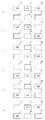
図7は、インバータ300の配線および半導体素子の配置を示す。図7において、配線層54f、54gは配線層50に含まれる配線層であって、配線層54eに対応する配線層である。配線層50、54のうち、実線の配線層は基板40(図7では不図示)に設けられ、点線の配線層は基板44(図7では不図示)に設けられていることを示す。すなわち、配線層50c、50dは基板40に、配線層54e〜54gは基板44に設けられている。また、半導体素子10〜31のうち、実線の半導体素子は高発熱主面が基板40側を向いて基板40に熱的に接続され、点線の半導体素子は高発熱主面が基板44側を向いて基板44に熱的に接続されていることを示す。すなわち、半導体素子10、20、30は基板44側を向いて基板44に熱的に接続され、半導体素子11、21、31は基板40側を向いて基板40に熱的に接続されている。また、図7において、U相端子120、V相端子121、W相端子122はそれぞれ、U、V、W相の出力端子である。
FIG. 7 shows the wiring of the
図8は、インバータ300の各相アームの概略断面図を示す。図8(a)は図7におけるA−A’断面であってU相アームおよびV相アームを含む概略断面を、図8(b)は図7におけるB−B’断面であってはW相アームの概略断面をそれぞれ示す。主面S20、S21、S30、S31はそれぞれ半導体素子20、21、30、31の高発熱主面を示す。図8に示すように、各相アームに含まれる2つの半導体素子は、その高発熱主面がそれぞれ異なる基板側を向いて設けられ、熱的に接続されている。また、ヒートスプレッダ61、62はヒートスプレッダ60に、ヒートスプレッダ65、66はヒートスプレッダ64にそれぞれ対応するヒートスプレッダである。また、配線層54f、54gは配線層54eに対応する配線層である。配線層54fは半導体素子20と半導体素子21を電気的に接続し、配線層54gは半導体素子30と半導体素子31をそれぞれ電気的に接続する。また、U相端子120、V相端子121、W相端子122は、外部の負荷500(図8(a)、図8(b)では不図示)に接続するための端子であり、それぞれ配線層54e、54f、54gに直に接して設けられている。なお、図8(a)、図8(b)では、実施の形態1の図1に示すような受動素子、制御回路素子の図示は省略している。
FIG. 8 is a schematic cross-sectional view of each phase arm of the
図9は、インバータ300により三相交流を生成する際の各半導体素子10〜31のオンオフとその配置関係を示す。図9における半導体素子10〜31の実線と点線の関係は図7と同様である。インバータ300は図示しない制御部により各半導体素子10〜31を図9(a)に示すオンオフ状態から図9(f)に示すオンオフ状態まで切り替えることにより三相交流を生成する。各相アームに含まれる2つの半導体素子の高発熱主面がそれぞれ異なる基板側を向いて設けられていることからも当然のように、高発熱主面が基板40側を向いて設けられている半導体素子と、高発熱主面が基板44側を向いて設けられている半導体素子とで均等にオンになっていることが図9からわかる。
FIG. 9 shows ON / OFF of each of the
以上の構成における電流の流れを図9(a)のオンオフ状態の場合、すなわち半導体素子10、21、30がオンで半導体素子11、20、31がオフの場合を例に説明する。
The current flow in the above configuration will be described by taking the case of the on / off state of FIG. 9A, that is, the case where the
まず、電流の大まかな流れを図6を用いて説明する。電源400からの電流は半導体素子10を通じて負荷500に流れる。同様に電源400からの電流は半導体素子30を通じて負荷500に流れる。負荷500に流れた電流は半導体素子21を通じて電源400に戻る。
First, a rough flow of current will be described with reference to FIG. A current from the
次に、図8(a)、図8(b)を用いて電流の流れをより具体的に説明する。電源400(図8(a)、図8(b)では不図示)からの電流は、入力端子124(図8(a)、図8(b)では不図示)から図8(a)の配線層50dに流れ込む。そして、半導体素子10を通じて配線層54eに流れ、U相端子120から負荷500(図8(a)、図8(b)では不図示)に流れ出る。同様に、電源400からの電流は、図8(b)の半導体素子30を通じて配線層54gに流れ、W相端子122から負荷500に流れ出る。半導体素子10および30を通じて負荷500に流れ出た電流は、図8(a)のV相端子121から配線層54fに流れ込む。そして、半導体素子21を通じて配線層50cに流れ、出力端子125(図8(a)、図8(b)では不図示)から電源400に戻る。
Next, the current flow will be described more specifically with reference to FIGS. 8A and 8B. The current from the power supply 400 (not shown in FIGS. 8A and 8B) is supplied from the input terminal 124 (not shown in FIGS. 8A and 8B) to the wiring in FIG. 8A. Flows into
実施の形態3によれば、各相アームに含まれる2つの半導体素子は高発熱主面がそれぞれ異なる基板側を向いて設けられ、熱的に接続されているため、それぞれの基板から半導体素子が発する熱を効率的に外部に放熱することが可能となり、インバータの放熱性能を向上させることができる。 According to the third embodiment, since the two semiconductor elements included in each phase arm are provided with the high heat generation main surfaces facing different substrate sides and thermally connected, the semiconductor elements are connected from the respective substrates. The generated heat can be efficiently dissipated to the outside, and the heat dissipation performance of the inverter can be improved.
(実施の形態4)
図10は実施の形態4に係るインバータの配線および半導体素子の配置を示し、図11は実施の形態4に係るインバータ300の各相アームの概略断面図を示す。図10、図11(a)〜(b)はそれぞれ図7、図8(a)〜(b)に対応する。実施の形態3と異なる箇所は、半導体素子20と半導体素子21の配置を逆にしていることと、配線層50cと配線層50dの形状が異なることである。
(Embodiment 4)
FIG. 10 shows the wiring of the inverter and the arrangement of the semiconductor elements according to the fourth embodiment, and FIG. 11 shows a schematic sectional view of each phase arm of the
図10に示すように、各半導体素子の高発熱主面は、異なる位相の半導体素子も含め、隣り合う半導体素子とは異なる基板側を向いて設けられ、熱的に接続されている。たとえば、図10に示すように、V相の半導体素子21の高発熱主面は基板40側を向いて設けられ、熱的に接続されている。一方、同じV相の半導体素子20の高発熱主面は基板44側を向いて設けられ、熱的に接続されている。また、U相およびW相の半導体素子であって半導体素子21と隣り合う半導体素子10、30の高発熱主面も基板44側を向いて設けられ、熱的に接続されている。
As shown in FIG. 10, the high heat generation main surface of each semiconductor element is provided facing the substrate side different from the adjacent semiconductor elements, including the semiconductor elements having different phases, and is thermally connected. For example, as shown in FIG. 10, the high heat generating main surface of the V-
また、図11に示すように、各半導体素子10〜31と配線層50、54の電気的な接続関係が実施の形態3と同じとなるように配線層50c、50dが形成されている。より具体的には、配線層50cは、半導体素子21、半導体素子11、半導体素子31がこの順番に配置されるように形成されている。同様に配線層50dは、半導体素子10、半導体素子30、半導体素子20がこの順番に配置されるように形成されている。また、配線層50cと配線層50dは重ならないように形成されている。
Also, as shown in FIG. 11, the wiring layers 50c and 50d are formed so that the electrical connection relationship between the
図12は、インバータ300により三相交流を生成する際の各半導体素子10〜31のオンオフとその配置関係を示す。図12(a)〜図12(f)は実施の形態3における図9(a)〜図9(f)に対応する図であり、実線と点線の関係は図9(a)〜図9(f)と同様である。各半導体素子10〜31を図12(a)に示すオンオフ状態から図12(f)に示すオンオフ状態まで切り替えることにより三相交流を生成する。
FIG. 12 shows ON / OFF of each of the
実施の形態4によれば、実施の形態3と同様の効果を奏する。それに加えて、隣り合う半導体素子の高発熱主面からの熱はそれぞれ異なる基板に主に放熱されるため、半導体素子の間隔を半導体素子1つ分大きく取った場合と同様に、半導体素子から生じた熱が基板の厚さ方向に伝わる間に重なり合って干渉し、局所的に大きな熱が発生する熱干渉を軽減でき、より効率的に放熱することが可能となる。 According to the fourth embodiment, the same effect as in the third embodiment is obtained. In addition, heat from the heat-generating main surfaces of adjacent semiconductor elements is mainly radiated to different substrates, so that the semiconductor elements are generated from the semiconductor elements as in the case where the distance between the semiconductor elements is increased by one semiconductor element. As the heat is transmitted in the thickness direction of the substrate, it overlaps and interferes, so that the heat interference caused by the generation of large heat can be reduced, and heat can be radiated more efficiently.
以上、本発明を実施例をもとに説明した。この実施例は例示であり、それらの各構成要素や各処理プロセスの組合せにいろいろな変形例が可能なこと、またそうした変形例も本発明の範囲にあることは当業者に理解されるところである。 In the above, this invention was demonstrated based on the Example. This embodiment is an exemplification, and it will be understood by those skilled in the art that various modifications can be made to the combination of each component and each processing process, and such modifications are also within the scope of the present invention. .
上述した実施の形態では、基板40、44として金属基板を用いる例を示したが、本発明はこれに限らない。たとえば、一方の基板にISB(Integrated System in Board;登録商標)基板を用いたり、基板内部にメタル板を挟み込んだメタルコア基板を用いてもよい。この場合、基板の熱伝導率が落ちるため熱を外部に放熱する効果は小さくなるが、高い集積能力が得られる。なお、ISB基板については特開2002−110717号公報に詳しい。
In the above-described embodiment, an example in which a metal substrate is used as the
また、図13に示すように、ヒートシンク層41、45およびサーマルビア42、46として金属(たとえばAg)を同時焼成したLTCC(Low Temperature Co-fired Ceramics)基板であってもよい。その場合、基板の厚み方向に貫通するサーマルビアは配線層50、54の無い部分に設ける。これにより絶縁性を保ちつつ、半導体素子が発する熱を外部に放熱することが可能となる。
Further, as shown in FIG. 13, an LTCC (Low Temperature Co-fired Ceramics) substrate obtained by simultaneously firing a metal (for example, Ag) as the heat sink layers 41 and 45 and the
また、上述した実施の形態では、半導体素子と配線層との間にヒートスプレッダを設ける例を示したが、ヒートスプレッダを設けずに、半導体素子の両主面が配線層に直に接するようにしてもよい。 Further, in the above-described embodiment, the example in which the heat spreader is provided between the semiconductor element and the wiring layer has been described. However, both main surfaces of the semiconductor element may be in direct contact with the wiring layer without providing the heat spreader. Good.
実施の形態2では、蛇腹構造のヒートスプレッダ60を各半導体素子の高発熱主面と反対の主面と配線層との間に設けられる例を示したが、高発熱主面と配線層との間に設けられてもよい。
In the second embodiment, the example in which the
また、実施の形態2では、ヒートスプレッダを蛇腹構造の弾性体とする例を示したが、これとは別に、弾性部材を半導体素子と基板との間に設けてもよい。なお、この場合、半導体素子と基板の間に設けられていればよく、半導体素子と弾性部材のいずれかに直に接していなくてもよい。 In the second embodiment, an example in which the heat spreader is an elastic body having a bellows structure has been described. Alternatively, an elastic member may be provided between the semiconductor element and the substrate. In this case, it may be provided between the semiconductor element and the substrate, and may not be in direct contact with either the semiconductor element or the elastic member.
実施の形態3および4では、U、V、W相の三相インバータの例を示したが、本発明はこれに限らない。たとえば、たとえば、単相または三相以外の多相インバータであってもよい。 In the third and fourth embodiments, an example of a U-phase, V-phase, and W-phase three-phase inverter is shown, but the present invention is not limited to this. For example, it may be a multiphase inverter other than a single phase or three phases.
10、11、20、21、30、31 半導体素子、 40、44 基板、 50、54 配線層、 60、64 ヒートスプレッダ、 70、74 受動素子 80、84 制御回路素子、 90 モールド樹脂、 200 半導体モジュール、 300 インバータ。
10, 11, 20, 21, 30, 31 Semiconductor element, 40, 44 Substrate, 50, 54 Wiring layer, 60, 64 Heat spreader, 70, 74
Claims (7)
前記第1の基板に対して所定の間隔で対向して配置されている第2の基板と、
前記第1の基板と前記第2の基板の間に設けられ、一方の主面側の発熱量が他方の主面側の発熱量より大きい第1の半導体素子と、
前記第1の基板と前記第2の基板の間に設けられ、一方の主面側の発熱量が他方の主面側の発熱量より大きい第2の半導体素子と、
を備え、
前記第1の半導体素子の一方の主面が前記第1の基板と熱的に接続し、
前記第2の半導体素子の一方の主面が前記第2の基板と熱的に接続していることを特徴とする半導体モジュール。 A first substrate;
A second substrate disposed facing the first substrate at a predetermined interval;
A first semiconductor element provided between the first substrate and the second substrate, wherein a heat generation amount on one main surface side is larger than a heat generation amount on the other main surface side;
A second semiconductor element provided between the first substrate and the second substrate, wherein a heat generation amount on one main surface side is larger than a heat generation amount on the other main surface side;
With
One main surface of the first semiconductor element is thermally connected to the first substrate;
A semiconductor module, wherein one main surface of the second semiconductor element is thermally connected to the second substrate.
Priority Applications (3)
| Application Number | Priority Date | Filing Date | Title |
|---|---|---|---|
| JP2011167683A JP2014199829A (en) | 2011-07-29 | 2011-07-29 | Semiconductor module and inverter mounting the same |
| PCT/JP2012/004809 WO2013018343A1 (en) | 2011-07-29 | 2012-07-27 | Semiconductor module and inverter having semiconductor module mounted thereon |
| US14/092,322 US9129933B2 (en) | 2011-07-29 | 2013-11-27 | Semiconductor module and an inverter mounting said semiconductor module |
Applications Claiming Priority (1)
| Application Number | Priority Date | Filing Date | Title |
|---|---|---|---|
| JP2011167683A JP2014199829A (en) | 2011-07-29 | 2011-07-29 | Semiconductor module and inverter mounting the same |
Publications (1)
| Publication Number | Publication Date |
|---|---|
| JP2014199829A true JP2014199829A (en) | 2014-10-23 |
Family
ID=47628894
Family Applications (1)
| Application Number | Title | Priority Date | Filing Date |
|---|---|---|---|
| JP2011167683A Withdrawn JP2014199829A (en) | 2011-07-29 | 2011-07-29 | Semiconductor module and inverter mounting the same |
Country Status (3)
| Country | Link |
|---|---|
| US (1) | US9129933B2 (en) |
| JP (1) | JP2014199829A (en) |
| WO (1) | WO2013018343A1 (en) |
Cited By (1)
| Publication number | Priority date | Publication date | Assignee | Title |
|---|---|---|---|---|
| US10076063B2 (en) | 2015-03-10 | 2018-09-11 | Toshiba Memory Corporation | Electronic apparatus |
Families Citing this family (15)
| Publication number | Priority date | Publication date | Assignee | Title |
|---|---|---|---|---|
| EP2963683B1 (en) * | 2013-02-28 | 2017-08-30 | Shindengen Electric Manufacturing Co. Ltd. | Module, module assembly, and module manufacturing method |
| DE102013212446A1 (en) * | 2013-06-27 | 2015-01-15 | Zf Friedrichshafen Ag | Electric circuit and method for producing an electrical circuit for driving a load |
| KR102222988B1 (en) | 2014-09-24 | 2021-03-04 | 삼성전자주식회사 | Multi-stacked structure of semiconductor packages |
| ITUB20153344A1 (en) * | 2015-09-02 | 2017-03-02 | St Microelectronics Srl | ELECTRONIC POWER MODULE WITH IMPROVED THERMAL DISSIPATION AND ITS MANUFACTURING METHOD |
| DE102016215982A1 (en) * | 2016-08-25 | 2018-03-01 | Siemens Aktiengesellschaft | Power module, manufacturing process and power electronics circuit |
| CN107612394B (en) * | 2017-09-12 | 2019-11-22 | 爱士惟新能源技术(江苏)有限公司 | Control processing method for the DC-to-AC converter with H5 topological structure |
| EP3481161A1 (en) * | 2017-11-02 | 2019-05-08 | AT & S Austria Technologie & Systemtechnik Aktiengesellschaft | Component carrier with transistor components arranged side by side |
| EP3598490A1 (en) * | 2018-07-18 | 2020-01-22 | Delta Electronics (Shanghai) Co., Ltd. | Power module |
| US11342241B2 (en) * | 2018-07-18 | 2022-05-24 | Delta Electronics (Shanghai) Co., Ltd | Power module |
| US11444036B2 (en) | 2018-07-18 | 2022-09-13 | Delta Electronics (Shanghai) Co., Ltd. | Power module assembly |
| EP4075498A3 (en) | 2018-07-18 | 2023-03-01 | Delta Electronics (Shanghai) Co., Ltd. | Power module structure |
| CN111384036B (en) * | 2018-12-28 | 2021-07-13 | 台达电子企业管理(上海)有限公司 | Power module |
| US11063525B2 (en) * | 2019-01-07 | 2021-07-13 | Delta Electronics (Shanghai) Co., Ltd. | Power supply module and manufacture method for same |
| TWI672711B (en) * | 2019-01-10 | 2019-09-21 | 健策精密工業股份有限公司 | Insulated metal substrate and manufacturing method thereof |
| EP3751605A1 (en) * | 2019-06-11 | 2020-12-16 | Siemens Aktiengesellschaft | Electronic switching circuit and method for producing same |
Family Cites Families (9)
| Publication number | Priority date | Publication date | Assignee | Title |
|---|---|---|---|---|
| JP3448159B2 (en) | 1996-06-20 | 2003-09-16 | 株式会社東芝 | Power semiconductor device |
| EP2234154B1 (en) * | 2000-04-19 | 2016-03-30 | Denso Corporation | Coolant cooled type semiconductor device |
| JP4192396B2 (en) | 2000-04-19 | 2008-12-10 | 株式会社デンソー | Semiconductor switching module and semiconductor device using the same |
| JP5029078B2 (en) | 2006-03-15 | 2012-09-19 | 株式会社日立製作所 | Power semiconductor device |
| US7557434B2 (en) | 2006-08-29 | 2009-07-07 | Denso Corporation | Power electronic package having two substrates with multiple electronic components |
| JP2008124430A (en) * | 2006-10-18 | 2008-05-29 | Hitachi Ltd | Power semiconductor module |
| JP2008227131A (en) | 2007-03-13 | 2008-09-25 | Renesas Technology Corp | Semiconductor device and its manufacturing method |
| JP5365627B2 (en) * | 2008-04-09 | 2013-12-11 | 富士電機株式会社 | Semiconductor device and manufacturing method of semiconductor device |
| JP2010225720A (en) * | 2009-03-23 | 2010-10-07 | Mitsubishi Electric Corp | Power module |
-
2011
- 2011-07-29 JP JP2011167683A patent/JP2014199829A/en not_active Withdrawn
-
2012
- 2012-07-27 WO PCT/JP2012/004809 patent/WO2013018343A1/en active Application Filing
-
2013
- 2013-11-27 US US14/092,322 patent/US9129933B2/en not_active Expired - Fee Related
Cited By (1)
| Publication number | Priority date | Publication date | Assignee | Title |
|---|---|---|---|---|
| US10076063B2 (en) | 2015-03-10 | 2018-09-11 | Toshiba Memory Corporation | Electronic apparatus |
Also Published As
| Publication number | Publication date |
|---|---|
| WO2013018343A1 (en) | 2013-02-07 |
| US20140077354A1 (en) | 2014-03-20 |
| US9129933B2 (en) | 2015-09-08 |
Similar Documents
| Publication | Publication Date | Title |
|---|---|---|
| JP2014199829A (en) | Semiconductor module and inverter mounting the same | |
| JP5975180B2 (en) | Semiconductor module | |
| CN105612613B (en) | Semiconductor device | |
| JP4973059B2 (en) | Semiconductor device and power conversion device | |
| KR100752239B1 (en) | Power module package structure | |
| WO2014014012A1 (en) | Power semiconductor module | |
| WO2004008532A2 (en) | High power mcm package | |
| CN104659012A (en) | Electronic component with electronic chip between redistribution structure and mounting structure | |
| JP2010129550A (en) | Power semiconductor module | |
| US10763244B2 (en) | Power module having power device connected between heat sink and drive unit | |
| JP5895220B2 (en) | Manufacturing method of semiconductor device | |
| JP2019071412A (en) | Chip package | |
| JP5481104B2 (en) | Semiconductor device | |
| CN111261598A (en) | Packaging structure and power module applicable to same | |
| JP2007123884A (en) | Power circuit package and method of fabricating same | |
| US9748205B2 (en) | Molding type power module | |
| US20150270201A1 (en) | Semiconductor module package and method of manufacturing the same | |
| WO2013118275A1 (en) | Semiconductor device | |
| JP2013041939A (en) | Semiconductor module and inverter mounting the same | |
| US11935807B2 (en) | Plurality of dies electrically connected to a printed circuit board by a clip | |
| JP5039388B2 (en) | Circuit equipment | |
| JP5682511B2 (en) | Semiconductor module | |
| JP2004048084A (en) | Semiconductor power module | |
| KR101897304B1 (en) | Power module | |
| JP6593630B2 (en) | Semiconductor module, drive device including the same, electric power steering device, and vehicle |
Legal Events
| Date | Code | Title | Description |
|---|---|---|---|
| A300 | Application deemed to be withdrawn because no request for examination was validly filed |
Free format text: JAPANESE INTERMEDIATE CODE: A300 Effective date: 20141104 |