US9719959B2 - Hydrogen ion sensor - Google Patents
Hydrogen ion sensor Download PDFInfo
- Publication number
- US9719959B2 US9719959B2 US14/546,476 US201414546476A US9719959B2 US 9719959 B2 US9719959 B2 US 9719959B2 US 201414546476 A US201414546476 A US 201414546476A US 9719959 B2 US9719959 B2 US 9719959B2
- Authority
- US
- United States
- Prior art keywords
- contact
- hydrogen ion
- bipolar junction
- gate insulation
- insulation layer
- Prior art date
- Legal status (The legal status is an assumption and is not a legal conclusion. Google has not performed a legal analysis and makes no representation as to the accuracy of the status listed.)
- Expired - Fee Related, expires
Links
Images


Classifications
-
- G—PHYSICS
- G01—MEASURING; TESTING
- G01N—INVESTIGATING OR ANALYSING MATERIALS BY DETERMINING THEIR CHEMICAL OR PHYSICAL PROPERTIES
- G01N27/00—Investigating or analysing materials by the use of electric, electrochemical, or magnetic means
- G01N27/26—Investigating or analysing materials by the use of electric, electrochemical, or magnetic means by investigating electrochemical variables; by using electrolysis or electrophoresis
- G01N27/28—Electrolytic cell components
- G01N27/30—Electrodes, e.g. test electrodes; Half-cells
-
- G—PHYSICS
- G01—MEASURING; TESTING
- G01N—INVESTIGATING OR ANALYSING MATERIALS BY DETERMINING THEIR CHEMICAL OR PHYSICAL PROPERTIES
- G01N27/00—Investigating or analysing materials by the use of electric, electrochemical, or magnetic means
- G01N27/26—Investigating or analysing materials by the use of electric, electrochemical, or magnetic means by investigating electrochemical variables; by using electrolysis or electrophoresis
- G01N27/403—Cells and electrode assemblies
- G01N27/414—Ion-sensitive or chemical field-effect transistors, i.e. ISFETS or CHEMFETS
Definitions
- the present invention relates to a hydrogen ion sensor, and more particularly, to a CMOS semiconductor hydrogen ion sensor based on a gated lateral bipolar junction transistor (GLBJT).
- a CMOS semiconductor hydrogen ion sensor based on a gated lateral bipolar junction transistor (GLBJT).
- GLBJT gated lateral bipolar junction transistor
- a hydrogen ion sensor is used for a purpose for measuring a concentration (for example, pH) of hydrogen ions for process control, a vivo assay and clinical analysis, an environmental monitoring or the like in various industry fields including chemical industry, public health, agriculture, fishery, and biology-related industry.
- pH is a parameter significantly considered when a characteristic of a solution to be measured is determined, and is an essential factor in understanding a chemical reaction or a chemical characteristic of a solution.
- a pH sensor is used for quantitatively measuring power of hydrogen (pH) that is a logarithm value of a hydrogen ion concentration of a solution to be measured.
- PH power of hydrogen
- the present invention provides a high sensitivity hydrogen ion sensor capable of remarkably improving sensitivity with respect to a hydrogen ion concentration.
- the present invention also provides a high sensitivity hydrogen ion sensor capable of quantitatively sensing the concentration of a trace of hydrogen ion.
- Embodiments of the present invention provide hydrogen ion sensor comprising: a substrate having a well and a first contact, the well having a second, a third, a fourth and a fifth contacts, the second contact having the same conductive type as the well, and the third, the fourth, and the fifth contacts having an opposite conductive type to the well; a first gate insulation layer on a region between the fourth contact and the fifth contact; a second gate insulation layer on a region between the third contact and the fourth contact; and a hydrogen ion sensing unit on the first gate insulation layer, wherein the hydrogen ion sensing unit transfers a voltage level adjusted according to a hydrogen ion concentration of a solution to be measured, to the first gate insulation layer.
- the hydrogen ion sensor may further comprise a first conductive layer on the first gate insulation layer; and a second conductive layer on the second gate insulation layer.
- the first gate insulation layer and the first conductive layer may have a ring shape surrounding the fifth contact
- the second gate insulation layer and the second conductive layer may have a ring shape surrounding the fourth contact
- the hydrogen ion sensing unit may comprise: a reference electrode contacting the solution to be measured, and to which a predetermined reference voltage is applied; a measurement electrode measuring the voltage level adjusted according to the hydrogen ion concentration; and a floating gate on the first gate insulation layer and transferring the voltage level to the first conductive layer.
- the measurement electrode may comprise; a first metal layer; and a passivation layer on the first metal layer, wherein the passivation layer comprises a silicon nitride layer.
- the floating gate may comprise a plurality of second metal layers connected to each other through vias.
- the well, the fourth contact, the fifth contact and the first gate insulation layer may constitute a first field effect transistor
- the well, the second contact, the fourth contact and the fifth contact may constitute a first bipolar junction transistor
- the substrate, the well, the first contact, the second contact and the fifth contact may constitute a second bipolar junction transistor
- the well, the third contact, the fourth contact, and the second gate insulation layer may constitute a second field effect transistor that is connected in a cascode structure to the first field effect transistor and the first bipolar junction transistor.
- the second filed effect transistor may be a field effect transistor of a N-channel type or a P-channel type.
- the first contact may operate as a collector terminal of the second bipolar junction transistor
- the second contact may operate as a base terminal of the first bipolar junction transistor and the second bipolar junction transistor
- the third contact may operate as a drain terminal of the second field effect transistor
- the fourth contact may operate as a drain terminal of the first field effect transistor, a source terminal of the second field effect transistor and a collector terminal of the first bipolar junction transistor
- the fifth contact may operate as a source terminal of the first field effect transistor and an emitter terminal of the first bipolar junction transistor and the second bipolar junction transistor.
- an operating point of the first bipolar junction transistor and the second bipolar junction transistor may be adjusted by a bias current applied on the second contact.
- the hydrogen ion concentration may be detected by detecting an amount of a current flowing through the fifth contact.
- FIG. 1 is a view illustrating a hydrogen ion sensing system including a hydrogen ion sensor according to an embodiment of the present invention
- FIG. 2 is a perspective view illustrating a hydrogen ion sensor according to an embodiment of the present invention
- FIG. 3 is a cross-sectional view illustrating a hydrogen ion sensor according to an embodiment of the present invention
- FIG. 4 is a view illustrating an equivalent circuit diagram of a hydrogen ion sensor according to an embodiment of the present invention
- FIG. 5 is a partial plane view illustrating a hydrogen ion sensor according to an embodiment of the present invention.
- FIG. 6 is a graph showing a change of transconductance of an existing hydrogen ion sensor with respect to each gate voltage
- FIG. 7 is a graph showing a change of transconductance of a hydrogen ion sensor according to an embodiment of the present invention with respect to each gate voltage;
- FIG. 8 is a graph showing a change of an emitter current of an existing hydrogen ion sensor with time
- FIG. 9 is a graph showing a change of an emitter current of a hydrogen ion sensor according to an embodiment of the present invention with time;
- FIG. 10 is a graph showing a comparison between sensitivity of an existing hydrogen ion sensor and sensitivity of a hydrogen ion sensor according to an embodiment of the present invention with time;
- FIG. 11 is a graph showing a change of an emitter current of an existing hydrogen ion sensor with time.
- FIG. 12 is a graph showing a change of an emitter current of a hydrogen ion sensor according to an embodiment of the present invention with time.
- a hydrogen ion sensor comprises a first conductive type substrate; a second conductive type well and a first conductive type first contact in the substrate; a second conductive type second contact, a third, a fourth and a fifth contacts of the first conductive type in the well; a first gate insulation layer on a region between the fourth contact and the fifth contact; a second gate insulation layer on a region between the third contact and the fourth contact; and a hydrogen sensing unit on the first gate insulation layer.
- the fourth contact and the fifth contact constitute a first field effect transistor
- the second contact, the fourth contact and the fifth contact constitute a first bipolar junction transistor
- the first contact, the second contact and the fifth contact constitute a second bipolar junction transistor.
- the hydrogen ion sensor according to an embodiment of the present invention is configured such that the third contact is disposed between the second contact and the fourth contact, and the third contact and the fourth contact constitute a second field effect transistor. Therefore, in the hydrogen ion sensor according to an embodiment of the present invention, since the second field effect transistor (the third and fourth contacts) is formed in a cascode series structure together with the first field effect transistor (the fourth and fifth contacts), the first bipolar junction transistor (the second, fourth and fifth contacts) and the second bipolar junction transistor (the first, second and fifth contacts), a transconductance characteristic of a CMOS element is improved, and thus a sensitivity characteristic with respect to a hydrogen ion is remarkably improved.
- FIG. 1 is a view illustrating a hydrogen ion sensing system including a hydrogen ion sensor according to an embodiment of the present invention.
- a hydrogen ion sensing system 10 may be provided as a semiconductor type hydrogen ion sensing system, and measure a hydrogen ion concentration (for example, pH) of a solution 20 to be measured.
- the solution 20 to be measured may be an electrolyte solution.
- the hydrogen ion sensing system 10 may include a hydrogen ion sensor 100 , a test fixture 200 , a semiconductor parameter analyzer 300 , and an analysis computer 400 .
- the hydrogen ion sensor 100 may be prepared by being manufactured in a chip type through a complementary metal-oxide semiconductor (CMOS) process and bonded on a printed circuit board (PCB), and may be sealed with an epoxy except for a hydrogen sensing unit (see reference numeral 160 of FIG. 2 ).
- CMOS complementary metal-oxide semiconductor
- PCB printed circuit board
- the test fixture 200 may apply a reference voltage to a reference electrode 161 in order to measure a hydrogen ion concentration of a solution 20 to be measured under an electric and optical shield environment, and receive a measurement value of the hydrogen ion sensor 100 outputted according to the hydrogen ion concentration of the solution 20 to be measured and supply the measurement value to the semiconductor parameter analyzer 300 .
- the semiconductor parameter analyzer 300 may measure the hydrogen ion concentration of the solution 20 to be measured by using the measurement value of the hydrogen ion sensor 100 , and supply an analysis result to the analysis computer 400 .
- the analysis computer 400 may display the hydrogen ion concentration of the solution 20 to be measured, or information on various parameters of the CMOS chip on a screen thereof.
- FIG. 2 is a cross-sectional view illustrating a hydrogen ion sensor according to an embodiment of the present invention.
- a hydrogen ion sensor 100 according to an embodiment of the present invention includes a substrate 110 , a well 120 , first to fifth contacts 131 to 135 , a first gate insulation layer 140 , a first conductive layer 141 , a second gate insulation layer 150 , a second conductive layer 151 and a hydrogen ion sensing unit 160 .
- the hydrogen ion sensor 100 has both of a characteristic of a bipolar junction transistor (BJT) and a characteristic of a metal oxide silicon field effect transistor (MOSFET), and may be provided in a gated lateral bipolar junction transistor (GLBJT) structure manufactured using CMOS process. This will be later described in more detail with reference to FIGS. 3 and 4 .
- BJT bipolar junction transistor
- MOSFET metal oxide silicon field effect transistor
- the substrate 110 may be a silicon substrate doped with a first conductive type (for example, a P conductive type) impurity.
- the well 120 may be provided in the substrate 110 .
- the well 120 may be provided in silicon doped with a second conductive type (for example, a N conductive type) impurity different from that of the substrate 110 .
- a Group V element such as phosphorus (P) may be injected into the substrate 110 to form the well 120 .
- the first contact 131 may be provided in an upper portion of a region except for the well 120 among regions on the substrate 110 .
- the first contact 131 may be provided in the silicon substrate doped with a first conductive type (for example, a P conductive type) impurity in the same manner as the substrate 110 .
- a Group III element such as boron (B) may be doped on the substrate 110 to form the first contact 131 .
- the first contact 131 may have a doping concentration higher than that of the substrate 110 . In an embodiment, the first contact 131 may be used as an electrode for forming a ground on the substrate 110 .
- the second to fifth contacts 132 to 135 may be provided on an upper portion of the well 120 .
- the third contact 133 , the fourth contact 134 and the fifth contact 135 may be sequentially provided in a direction directed from the second contact 132 to the fifth contact 135 .
- the fourth contact 134 may be disposed on a position spaced apart from the fifth contact 135 while surrounding the fifth contact 135 in a ring shape
- the third contact 133 may be disposed on a position spaced apart from the fourth contact 134 while surrounding the fourth contact 134 in a ring shape
- the second contact 132 may be disposed on a position spaced apart from the third contact 133 while surrounding the third contact 133 in a ring shape.
- the second contact 132 may be provided in the silicon substrate doped with a second conductive type (for example, a N conductive type) impurity in the same manner as the well 120 .
- a second conductive type for example, a N conductive type
- a Group V element such as phosphorus (P) may be doped on an upper portion the well 110 to form the second contact 132 .
- the second contact 132 may have a doping concentration higher than that of the well 120 .
- the second contact 132 may be used as an electrode supplying electric power (for example, a base current) to the well 120 .
- the third to fifth contacts 133 to 135 may be provided in the silicon doped with a first conductive type (for example, a P conductive type) impurity in the same manner as the substrate 110 .
- a Group III element such as boron (B) may be doped on an upper portion of the well 120 to form third to fifth contacts 133 and 135 .
- the first gate insulation layer 140 may be disposed on a region between the fourth contact 134 and the fifth contact 135 .
- the first conductive layer 141 may be disposed on the first gate insulation layer 140 .
- the first gate insulation layer 140 and the first conductive layer 141 may be formed so as to have a ring shape surrounding the fifth contact 135 .
- the second gate insulation layer 150 may be disposed on a region between the third contact 133 and the fourth contact 134 .
- the second conductive layer 151 may be disposed on the second gate insulation layer 150 .
- the second gate insulation layer 150 and the second conductive layer 151 may be formed so as to have a ring shape surrounding the fourth contact 134 .
- the first and second gate insulation layers 140 and 150 may include silicon oxide (SiO 2 ).
- the first and second conductive layers 141 and 151 may include poly silicon.
- the hydrogen ion sensing unit 160 may be disposed on the first conductive layer 141 .
- the hydrogen ion sensing unit 160 may transfer a voltage level adjusted according to a hydrogen ion concentration of the solution (see reference numeral 20 of FIG. 1 ) to be measured to the first conductive layer 141 and the first gate insulation layer 140 .
- the hydrogen ion sensing unit 160 may include a reference electrode 161 , a measurement electrode 162 and a floating gate 163 .
- the reference electrode 161 may be provided to contact the solution 20 to be measured and to be spaced apart from the measurement electrode 162 .
- a predetermined reference voltage may be applied on the reference electrode 161 .
- the reference electrode 161 may be provided in the form of a conductive material, such as silver (Ag)/silver chloride (AgCl), gold (Au), palladium (Pd), platinum (Pt) or the like, for example, a precious metal.
- a surface potential of the measurement electrode 162 may be adjusted according to a hydrogen ion concentration.
- the surface potential of the measurement electrode 162 is changed according to a hydrogen ion concentration of the solution 20 to be measured by an electrochemical reaction, and thus the hydrogen ion concentration may be measured from a change of a current amount that flows in the fifth contact 135 .
- the measurement electrode 162 may include a metal, such as gold (Au), palladium (Pd) or platinum (Pt).
- the measurement electrode 162 may be formed so as to have an area greater than that of the first conductive layer 141 operating as a gate terminal G, and thus detection performance of the hydrogen ion sensor 100 may be improved.
- the measurement electrode 162 may be provided with a metal layer 1621 and a passivation layer 1622 .
- the passivation layer 1622 may be disposed on an upper portion of the metal layer 1621 , and may be stacked through a method such as a plasma enhanced chemical vapor deposition in a commonly used CMOS process.
- the passivation layer 1622 may include a silicon nitride layer (for example, Si 3 N 4 ) or Al 2 O 3 .
- the passivation layer 1622 may induce a site-binding phenomenon, and a potential of the floating gate 163 may be changed according to a change of the surface potential.
- the floating gate 163 is disposed on the first conductive layer 141 so as to operate as an ion detection gate, and transfers a voltage level applied on the measurement electrode 162 , to the first conductive layer 141 and the first gate insulation layer 140 .
- the floating gate 163 may be comprised of a plurality of metal layers 1632 connected to each other through vias 1631 .
- a floating gate 163 structure is suitably applied to a process having a gate width that is a nano unit compared to an open gate structure.
- FIG. 3 is a cross-sectional view illustrating a hydrogen ion sensor according to an embodiment of the present invention.
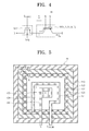
- FIG. 4 is a view illustrating an equivalent circuit diagram of a hydrogen ion sensor according to an embodiment of the present invention.
- the second field effect transistor FET 2 constituted by the well 120 , the third contact 133 , the fourth contact 134 , the second gate insulation layer 150 and the second conductive layer 151 is connected to the first field effect transistor FET 1 and the first bipolar junction transistor BJT 1 in series in a cascode structure.
- the minimum of the hydrogen ion concentration may be quantitatively sensed.
- the well 120 may operate as a body of the first field effect transistor FET 1
- the fourth contact 134 and the fifth contact 135 may operate as a drain terminal and a source terminal of the first field effect transistor FET 1 respectively
- the first gate insulation layer 140 may operate as a gate insulation layer of the first field effect transistor FET 1
- the first conductive layer 141 may operate as a gate terminal of the first field effect transistor FET 1
- the well 120 , the fourth contact 134 , the fifth contact 135 , the first gate insulation layer 140 and the first conductive layer 141 may operate as a P-channel type field effect transistor.
- the first field effect transistor FET 1 may be designed in a N-channel type field effect transistor.
- the well 120 and the second contact 132 may operate as a base terminal B of the first bipolar junction transistor BJT 1
- the fourth contact 134 may operate as a collector terminal C of the first bipolar junction transistor BJT 1
- the fifth contact 135 may operate as an emitter terminal E of the first bipolar junction transistor BJT 1 . Since the collector terminal C and the emitter terminal E of the first bipolar junction transistor BJT 1 constituted by the well 120 , the second contact 132 , the fourth contact 134 and the fifth contact 135 are disposed in a lateral shape, the first bipolar junction transistor BJT 1 may be called a lateral junction transistor.
- the substrate 110 , the well 120 and the second contact 132 may operate as a base terminal B of the second bipolar junction transistor BJT 2
- the first contact 131 may operate as a collector terminal S of the second bipolar junction transistor BJT 2
- the fifth contact 135 may operate as an emitter terminal E of the second bipolar junction transistor BJT 2 . Since the collector terminal S and the emitter terminal E of the second bipolar junction transistor BJT 2 constituted by the substrate 110 , the well 120 , the first contact 131 , the second contact 132 and the fifth contact 135 are disposed in a vertical shape, the second bipolar junction transistor BJT 2 may be called as a vertical junction transistor.
- the well 120 may operate as a body of the second field effect transistor FET 2
- the third contact 133 and the fourth contact 134 may operate as a drain terminal D and a source terminal of the second field effect transistor FET 2
- the second gate insulation layer 150 may operate as a gate insulation layer of the second field effect transistor FET 2
- the second conductive layer 151 may be operate as a gate terminal G CASCODE of the second field effect transistor FET 2
- the well 120 , the third contact 133 , the fourth contact 134 , the second insulation layer 150 and the second conductive layer 151 may operate as a P-channel type effect transistor.
- the second field effect transistor FET 2 may be designed in a N-channel type effect transistor.
- Flows of a channel current C 1 of the first field effect transistor FET 1 , a channel current C 5 of the second field effect transistor FET 2 , an emitter current (Ie) C 2 of the first bipolar junction transistor BJT 1 , a base current C 3 flowing into a base terminal of the first bipolar junction transistor BJT 1 and the second bipolar junction transistor BJT 2 , and a collector current C 4 of the second bipolar junction transistor BJT 2 are illustrated in a dashed line arrow in FIG. 2 .
- a portion except for the hydrogen ion sensing unit 160 that is, a portion including the substrate 110 , the well 120 , the first to fifth contacts 131 to 135 , the first and second gate insulation layers 140 and 160 , and the first and second conductive layers 141 and 151 may be called a transistor unit TR.
- the hydrogen sensing unit 100 may operate in an FET mode, a BJT mode or a hybrid mode.
- the first and second field effect transistors FET 1 and FET 2 may not operate in the BJT mode.
- a positive voltage is applied on the reference electrode 161
- the positive voltage is transferred to the gate terminal of the first field effect transistor FET 1 from the reference electrode 161 through the solution 20 to be measured
- a channel may not be formed in the first field effect transistor FET 1 . Therefore, the first field effect transistor FET 1 may maintain a turn-off state regardless of whether or not a hydrogen ion exists in the solution 20 to be measured.
- the first and second bipolar junction transistors BJT 1 and BJT 2 are forward-biased.
- the hydrogen ion sensor 100 may show an operation characteristic according a structure itself of the hydrogen ion sensor 100 regardless of whether or not a hydrogen ion exists in the solution 20 to be measured. Therefore, the BJT mode may be used as a pilot mode detecting an operation characteristic of the hydrogen ion sensor 100 itself.
- the first and second bipolar junction transistors BJT 1 and BJT 2 do not operate in the FET mode. For example, when a current is introduced into the second contact 132 operating as the base terminal of the first and second bipolar junction transistors BJT 1 and BJT 2 , the first and second bipolar junction transistors BJT 1 and BJT 2 are reverse-biased. When a negative voltage is applied on the reference electrode 161 , a negative voltage is transferred to the gate terminal of the first field effect transistor FET 1 from the reference electrode 161 through the solution 20 to be measured. That is, the first field effect transistor FET 1 may change an amount of a channel current according to a hydrogen ion concentration in the solution 20 to be measured.
- all of the first and second bipolar junction transistors BJT 1 and BJT 2 , and the first and second field effect transistors FET 1 and FET 2 operate.
- the first and second bipolar junction transistors BJT 1 and BJT 2 are forward-biased, and when a negative voltage is applied on the reference electrode 161 at the same time, the first field effect transistor FET 1 changes an amount of a channel current according to a hydrogen ion concentration in the solution 20 to be measured.
- a current flowing between the fifth contact 135 and the fourth contact 134 may be represented in a sum of a current flow by the first and second bipolar junction transistors BJT 1 and BJT 2 and a current flow by the first field effect transistor FET 1 . Therefore, when the first and second bipolar junction transistors BJT 1 and BJT 2 are forward-biased by a base current Ib, the hydrogen ion sensor 100 operates like a depletion type field effect transistor.
- An operating point of the first and second bipolar junction transistors BJT 1 and BJT 2 may be adjusted by a bias current applied on the second contact 132 .
- the fifth contact 135 operating as the emitter terminal E may be provided with a voltage source applying an emitter voltage on the fifth contact 135 .
- the first contact 131 operating as the collector terminal S may be connected to a ground node.
- the fifth contact 135 operating as the emitter terminal E may be used as a sensing node.
- the hydrogen ion sensor 100 may detect the emitter current Ie flowing into the fifth contact 135 to detect a hydrogen ion concentration in the solution 20 to be measured.
- An operating point (or sensitivity) of the hydrogen ion sensor 100 may be adjusted by changing a reference voltage applied on the reference electrode 161 or changing a base current biased to the second contact 132 operating as the base terminal B.
- FIG. 5 is a partial plane view illustrating a hydrogen ion sensor according to an embodiment of the present invention.
- FIG. 5 illustrates a plane layout of a hydrogen ion sensor 100 except for a hydrogen ion sensing unit 160 , that is, a transistor unit TR.
- the transistor unit TR may be manufactured through a CMOS process.
- the fifth contact 135 operating as the emitter terminal E of the first and second bipolar junction transistors BJT 1 and BJT 2 and the source terminal of the first field effect transistor FET 1 is disposed on a center.
- the first gate insulation layer 140 operating as the gate insulation layer of the first field effect transistor FET 1 and the first conductive layer 141 operating as the gate terminal G of the first field effect transistor FET 1 are disposed in a ring shape (for example, a square ring) outside the fifth contact 135 .
- the fourth contact 134 operating as the collector terminal C of the first bipolar junction transistors BJT 1 and the drain terminal of the first field effect transistor FET 1 and the source terminal of the second field effect transistor FET 2 is disposed in a shape ring (for example, a square ring) outside the first conductive layer 141 .
- the second gate insulation layer 150 operating as the gate insulation layer of the second field effect transistor FET 2 and the second conductive layer 151 operating as the gate terminal G CASCODE of the second field effect transistor FET 2 are disposed in a ring shape (for example, a square ring) outside the fourth contact 134 .
- the third contact 133 operating as the drain terminal D of the second field effect transistor FET 2 is disposed in a ring shape (for example, a square ring) outside the second conductive layer 151 .
- the second contact 132 operating as the base terminal of the first and second bipolar junction transistors BJT 1 and BJT 2 is disposed in a ring shape (for example, a square ring) outside the third contact 133 .
- the well 120 operating as the base terminal of the first and second bipolar junction transistors BJT 1 and BJT 2 is disposed outside the second contact 132 .
- the substrate 110 operating as the collector terminal of the second bipolar junction transistor BJT 2 is disposed outside the well 120 .
- the first contact 131 operating as the collector terminal S of the second bipolar junction transistor BJT 2 may be disposed on the substrate 110 .
- FIG. 6 is a graph showing a change of transconductance of an existing hydrogen ion sensor with respect to each gate voltage
- FIG. 7 is a graph showing a change of transconductance of a hydrogen ion sensor according to an embodiment of the present invention with respect to each gate voltage.
- a gated lateral bipolar junction transistor not including the third contact 133 , the second gate insulation layer 150 and the second conductive layer 151 was used as an existing hydrogen ion sensor. That is, the existing hydrogen ion sensor used a structure in which the second field effect transistor FET 2 was not connected to the first field effect transistor FET 1 and the first bipolar junction transistor BJT 1 in a cascode.
- a base current Ib of the base terminal was changed in a range of about ⁇ 150 ⁇ m to about 150 ⁇ m
- a voltage V G of the gate terminal was changed in a range of about ⁇ 12 to about 2 V in a case of the existing hydrogen ion sensor
- a voltage V G of the gate terminal was changed in a range of about ⁇ 4 to about 2 V in a case of the hydrogen ion sensor according to an embodiment of the present invention.
- transconductance g m was improved by about three times greater in average than that of the existing hydrogen ion sensor in which the second field effect transistor was not connected in the cascode. This result means that the hydrogen ion sensor 100 according to an embodiment of the present invention may much more sensitively detect the hydrogen ion.
- FIG. 8 is a graph showing a change of an emitter current of an existing hydrogen ion sensor according to a time
- FIG. 9 is a graph showing a change of an emitter current of a hydrogen ion sensor according to an embodiment of the present invention with time.
- a solution to be measured having a pH of about 5.0, a solution to be measured having a pH of about 7.0 and a solution to be measured having a pH of about 9.18 were sequentially supplied, and an emitter current Ie flowing into the emitter terminal E was measured.
- the concentration of hydrogen ion that is, the higher pH value is, the more an emitter current Ie is increased.
- FIGS. 8 and 9 the lower the concentration of hydrogen ion is, that is, the higher pH value is, the more an emitter current Ie is increased.
- a change width of the emitter current is much greater than that of the existing hydrogen ion sensor in which the second field effect transistor was not connected in the cascode. This means that the hydrogen ion sensor 100 according to an embodiment of the present invention may more sensitively detect a pH change.
- FIG. 10 is a graph showing a comparison between sensitivity of an existing hydrogen ion sensor and sensitivity of a hydrogen ion sensor according to an embodiment of the present invention with time.
- the sensitivity of the hydrogen ion sensor was calculated from a ratio of a change amount of the emitter current Ie with respect to a pH change amount of a solution to be measured. As shown in FIG.
- the sensitivity of the hydrogen ion sensor according to an embodiment of the present invention is improved by about 4.5 times greater than the existing hydrogen ion sensor in which the second field effect transistor (the third contact, the second gate insulation layer and the second conductive layer) was not connected in the cascode.
- FIG. 11 is a graph showing a change of an emitter current of an existing hydrogen ion sensor with time
- FIG. 12 is a graph showing a change of an emitter current of a hydrogen ion sensor according to an embodiment of the present invention with time.
- An emitter current that was measured while pH of a solution to be measured was changed in a range of about 1.68 to about 12.46, and as a result, it may be seen that a change width of an emitter current Ie in the hydrogen ion sensor according to an embodiment of the present invention is improved by about 3 times greater than the existing hydrogen ion sensor in which the second field effect transistor FET 2 was not connected in the cascode.
- the second field effect transistor FET 2 is connected to the first field effect transistor FET 1 and the first and second bipolar junction transistors BJT 1 and BJT 2 in a cascode structure in series, thereby capable of obtaining the hydrogen ion sensor having high sensitivity with respect to a hydrogen ion concentration.
- a high sensitivity hydrogen ion sensor capable of remarkably improving sensitivity with respect to a hydrogen ion concentration.
- a high sensitivity hydrogen ion sensor capable of quantitatively sensing the minimum of a hydrogen ion concentration.
Landscapes
- Health & Medical Sciences (AREA)
- Life Sciences & Earth Sciences (AREA)
- Chemical & Material Sciences (AREA)
- General Physics & Mathematics (AREA)
- Physics & Mathematics (AREA)
- Electrochemistry (AREA)
- Pathology (AREA)
- Analytical Chemistry (AREA)
- Biochemistry (AREA)
- General Health & Medical Sciences (AREA)
- Molecular Biology (AREA)
- Immunology (AREA)
- Chemical Kinetics & Catalysis (AREA)
- Engineering & Computer Science (AREA)
- Microelectronics & Electronic Packaging (AREA)
- Investigating Or Analyzing Materials By The Use Of Electric Means (AREA)
- Power Engineering (AREA)
- Ceramic Engineering (AREA)
- Condensed Matter Physics & Semiconductors (AREA)
- Computer Hardware Design (AREA)
Applications Claiming Priority (2)
| Application Number | Priority Date | Filing Date | Title |
|---|---|---|---|
| KR10-2013-0140109 | 2013-11-18 | ||
| KR1020130140109A KR101515491B1 (ko) | 2013-11-18 | 2013-11-18 | 수소이온 감지센서 |
Publications (2)
| Publication Number | Publication Date |
|---|---|
| US20150137190A1 US20150137190A1 (en) | 2015-05-21 |
| US9719959B2 true US9719959B2 (en) | 2017-08-01 |
Family
ID=53172398
Family Applications (1)
| Application Number | Title | Priority Date | Filing Date |
|---|---|---|---|
| US14/546,476 Expired - Fee Related US9719959B2 (en) | 2013-11-18 | 2014-11-18 | Hydrogen ion sensor |
Country Status (2)
| Country | Link |
|---|---|
| US (1) | US9719959B2 (ko) |
| KR (1) | KR101515491B1 (ko) |
Cited By (2)
| Publication number | Priority date | Publication date | Assignee | Title |
|---|---|---|---|---|
| US10957787B2 (en) | 2019-03-12 | 2021-03-23 | Globalfoundries Singapore Pte. Ltd. | Sensors based on a heterojunction bipolar transistor construction |
| US11016055B2 (en) | 2019-07-09 | 2021-05-25 | Globalfoundries Singapore Pte. Ltd. | Sensors with a front-end-of-line solution-receiving cavity |
Families Citing this family (4)
| Publication number | Priority date | Publication date | Assignee | Title |
|---|---|---|---|---|
| JP6554533B2 (ja) * | 2015-03-02 | 2019-07-31 | 株式会社半導体エネルギー研究所 | 環境センサ |
| US9659979B2 (en) | 2015-10-15 | 2017-05-23 | International Business Machines Corporation | Sensors including complementary lateral bipolar junction transistors |
| JP2019056581A (ja) * | 2017-09-20 | 2019-04-11 | ソニーセミコンダクタソリューションズ株式会社 | 電荷検出センサおよび電位計測システム |
| KR20220107377A (ko) | 2021-01-25 | 2022-08-02 | 금오공과대학교 산학협력단 | 인듐주석 산화물을 이용한 이온 검출 센서 |
Citations (4)
| Publication number | Priority date | Publication date | Assignee | Title |
|---|---|---|---|---|
| KR101050761B1 (ko) | 2010-02-19 | 2011-07-21 | 경북대학교 산학협력단 | 배열형 수평 바이폴라 트랜지스터를 이용한 수소이온 감지소자 |
| KR20110122323A (ko) | 2010-05-04 | 2011-11-10 | 경북대학교 산학협력단 | 이중 게이트를 갖는 수평형 바이폴라 접합 트랜지스터를 이용한 이온 감지소자 |
| KR20120000369A (ko) | 2010-06-25 | 2012-01-02 | 경북대학교 산학협력단 | 바이오 센서 및 이를 이용한 바이오 물질 검출 방법 |
| KR20120038041A (ko) | 2010-10-12 | 2012-04-23 | 경북대학교 산학협력단 | 반도체 소자를 이용한 휘발성 유기화합물 가스 감지장치 및 이를 이용한 휘발성 유기화합물 가스 감지방법 |
-
2013
- 2013-11-18 KR KR1020130140109A patent/KR101515491B1/ko active IP Right Grant
-
2014
- 2014-11-18 US US14/546,476 patent/US9719959B2/en not_active Expired - Fee Related
Patent Citations (5)
| Publication number | Priority date | Publication date | Assignee | Title |
|---|---|---|---|---|
| KR101050761B1 (ko) | 2010-02-19 | 2011-07-21 | 경북대학교 산학협력단 | 배열형 수평 바이폴라 트랜지스터를 이용한 수소이온 감지소자 |
| US8283736B2 (en) * | 2010-02-19 | 2012-10-09 | Kyungpook National University Industry Academic Cooperation | Hydrogen ion sensing device using of arrayed gated lateral BJT |
| KR20110122323A (ko) | 2010-05-04 | 2011-11-10 | 경북대학교 산학협력단 | 이중 게이트를 갖는 수평형 바이폴라 접합 트랜지스터를 이용한 이온 감지소자 |
| KR20120000369A (ko) | 2010-06-25 | 2012-01-02 | 경북대학교 산학협력단 | 바이오 센서 및 이를 이용한 바이오 물질 검출 방법 |
| KR20120038041A (ko) | 2010-10-12 | 2012-04-23 | 경북대학교 산학협력단 | 반도체 소자를 이용한 휘발성 유기화합물 가스 감지장치 및 이를 이용한 휘발성 유기화합물 가스 감지방법 |
Non-Patent Citations (9)
| Title |
|---|
| Kwon et al., "The Characteristics of H + Ion-Sensitive Transistor Driving With MOS Hybrid Mode Operation", IEEE Electron Device Letters, vol. 29, No. 10, Oct. 2008, pp. 1138-1141. |
| Lin et al., "Lateral Complementary Transistor Structure for the Simultaneous Fabrication of Functional Blocks", Proceedings of the IEEE, Dec. 1964, pp. 1491-1496. |
| Parke et al., "Bipolar-FET Hybrid-Mode Operation of Quarter-Micrometer SOI MOSFET's", IEEE Electron Device Letters, vol. 14, No. 5, May 1993, pp. 234-236. |
| Shine et al., "Solid phase radioimmunoassay for human C-reactive protein", Clinicu Chimicu Acta, 117 (1981), pp. 13-23. |
| Wong, "Matching Properties and Applications of Compatible Lateral Bipolar Transistors (CLBTs)", A Thesis Submitted in Partial Fulfillment of the Requirements for the Degree of Master of Philosophy in the Computer Science and Engineering Department, The Chinese University of Hong Kong, Jul. 2001, pp. 1-111. |
| Yuan et al., "Highly sensitive ion sensor based on the MOSFET-BJT hybrid mode of a gated lateral BJT", Sensors and Actuators B 181 (2013), pp. 44-49. |
| Yuan et al., "MOSFET-BJT hybrid mode of the gated lateral bipolar junction transistor for C-reactive protein detection", Biosensors and Bioelectronics 28 (2011) 434-437. |
| Yuan et al., "Room temperature VOC gas detection using a gated lateral BJT with an assembled solvatochromic dye", Sensors and Actuators B 187 (2013), pp. 288-294. |
| Yuan et al., "Sensitivity Alterable Biosensor Based on Gated Lateral BJT for CRP Detection", Journal of Semiconductor Technology and Science, vol. 13, No. 1, Feb. 2013, pp. 434-437. |
Cited By (2)
| Publication number | Priority date | Publication date | Assignee | Title |
|---|---|---|---|---|
| US10957787B2 (en) | 2019-03-12 | 2021-03-23 | Globalfoundries Singapore Pte. Ltd. | Sensors based on a heterojunction bipolar transistor construction |
| US11016055B2 (en) | 2019-07-09 | 2021-05-25 | Globalfoundries Singapore Pte. Ltd. | Sensors with a front-end-of-line solution-receiving cavity |
Also Published As
| Publication number | Publication date |
|---|---|
| KR101515491B1 (ko) | 2015-05-06 |
| US20150137190A1 (en) | 2015-05-21 |
Similar Documents
| Publication | Publication Date | Title |
|---|---|---|
| US9719959B2 (en) | Hydrogen ion sensor | |
| US11008611B2 (en) | Double gate ion sensitive field effect transistor | |
| TWI422818B (zh) | 氫離子感測場效電晶體及其製造方法 | |
| US8283736B2 (en) | Hydrogen ion sensing device using of arrayed gated lateral BJT | |
| CN101501481B (zh) | 纳米结构传感器 | |
| JP6731846B2 (ja) | 電荷検出のための集積センサデバイス | |
| KR101217576B1 (ko) | 바이오 센서 및 그의 구동 방법 | |
| US8698210B2 (en) | Sensor and method for manufacturing the same | |
| WO2010125717A1 (ja) | 化学センサ | |
| US20130056353A1 (en) | Ion sensitive detector | |
| TW201225304A (en) | Chemically sensitive sensor with lightly doped drains | |
| JP2008215974A (ja) | 電界効果トランジスタ型イオンセンサ | |
| EP3042214B1 (en) | Low offset and high sensitivity vertical hall effect sensor | |
| US11293897B2 (en) | High sensitivity ISFET sensor | |
| CN107543853B (zh) | 电化学检测器 | |
| Zhao et al. | Floating-Gate Ion Sensitive Field-Effect Transistor for Chemical and Biological Sensing | |
| US8795511B2 (en) | Configuration, a sensing element with such configuration, electrochemical sensor comprising such sensing element and method for electrochemical sensing using such electrochemical sensor | |
| KR101204333B1 (ko) | 바이오 센서 및 이를 이용한 바이오 물질 검출 방법 | |
| KR101729685B1 (ko) | 이온 농도 검출 방법 및 장치 | |
| KR101128855B1 (ko) | 이중 게이트를 갖는 수평형 바이폴라 접합 트랜지스터를 이용한 이온 감지소자 | |
| US8410530B2 (en) | Sensitive field effect transistor apparatus | |
| US20230133476A1 (en) | Time-Resolved Multi-Gate Ion Sensitive Field Effect Transducer and System and Method of Operating the Same | |
| CN114624308A (zh) | 离子传感设备 | |
| JP2013019851A (ja) | 半導体センサ |
Legal Events
| Date | Code | Title | Description |
|---|---|---|---|
| AS | Assignment |
Owner name: KYUNGPOOK NATIONAL UNIVERSITY INDUSTRY-ACADEMIC CO Free format text: ASSIGNMENT OF ASSIGNORS INTEREST;ASSIGNORS:KANG, SHIN-WON;JEONG, HYUN-MIN;YUN, HYEON-JI;AND OTHERS;REEL/FRAME:034199/0798 Effective date: 20141117 |
|
| STCF | Information on status: patent grant |
Free format text: PATENTED CASE |
|
| FEPP | Fee payment procedure |
Free format text: MAINTENANCE FEE REMINDER MAILED (ORIGINAL EVENT CODE: REM.); ENTITY STATUS OF PATENT OWNER: SMALL ENTITY |
|
| LAPS | Lapse for failure to pay maintenance fees |
Free format text: PATENT EXPIRED FOR FAILURE TO PAY MAINTENANCE FEES (ORIGINAL EVENT CODE: EXP.); ENTITY STATUS OF PATENT OWNER: SMALL ENTITY |
|
| STCH | Information on status: patent discontinuation |
Free format text: PATENT EXPIRED DUE TO NONPAYMENT OF MAINTENANCE FEES UNDER 37 CFR 1.362 |
|
| FP | Lapsed due to failure to pay maintenance fee |
Effective date: 20210801 |