US9655248B2 - Method of manufacturing a wiring board - Google Patents
Method of manufacturing a wiring board Download PDFInfo
- Publication number
- US9655248B2 US9655248B2 US14/468,707 US201414468707A US9655248B2 US 9655248 B2 US9655248 B2 US 9655248B2 US 201414468707 A US201414468707 A US 201414468707A US 9655248 B2 US9655248 B2 US 9655248B2
- Authority
- US
- United States
- Prior art keywords
- insulating layer
- metallic foil
- cavity
- separable
- wiring
- Prior art date
- Legal status (The legal status is an assumption and is not a legal conclusion. Google has not performed a legal analysis and makes no representation as to the accuracy of the status listed.)
- Expired - Fee Related, expires
Links
Images


Classifications
-
- H—ELECTRICITY
- H05—ELECTRIC TECHNIQUES NOT OTHERWISE PROVIDED FOR
- H05K—PRINTED CIRCUITS; CASINGS OR CONSTRUCTIONAL DETAILS OF ELECTRIC APPARATUS; MANUFACTURE OF ASSEMBLAGES OF ELECTRICAL COMPONENTS
- H05K1/00—Printed circuits
- H05K1/18—Printed circuits structurally associated with non-printed electric components
- H05K1/182—Printed circuits structurally associated with non-printed electric components associated with components mounted in printed circuit boards [PCB], e.g. insert-mounted components [IMC]
- H05K1/185—Printed circuits structurally associated with non-printed electric components associated with components mounted in printed circuit boards [PCB], e.g. insert-mounted components [IMC] associated with components encapsulated in the insulating substrate of the PCBs; associated with components incorporated in internal layers of multilayer circuit boards
-
- H01L2224/16225—
-
- H—ELECTRICITY
- H05—ELECTRIC TECHNIQUES NOT OTHERWISE PROVIDED FOR
- H05K—PRINTED CIRCUITS; CASINGS OR CONSTRUCTIONAL DETAILS OF ELECTRIC APPARATUS; MANUFACTURE OF ASSEMBLAGES OF ELECTRICAL COMPONENTS
- H05K2203/00—Indexing scheme relating to apparatus or processes for manufacturing printed circuits covered by H05K3/00
- H05K2203/13—Moulding and encapsulation; Deposition techniques; Protective layers
- H05K2203/1305—Moulding and encapsulation
- H05K2203/1322—Encapsulation comprising more than one layer
-
- H—ELECTRICITY
- H05—ELECTRIC TECHNIQUES NOT OTHERWISE PROVIDED FOR
- H05K—PRINTED CIRCUITS; CASINGS OR CONSTRUCTIONAL DETAILS OF ELECTRIC APPARATUS; MANUFACTURE OF ASSEMBLAGES OF ELECTRICAL COMPONENTS
- H05K3/00—Apparatus or processes for manufacturing printed circuits
- H05K3/02—Apparatus or processes for manufacturing printed circuits in which the conductive material is applied to the surface of the insulating support and is thereafter removed from such areas of the surface which are not intended for current conducting or shielding
- H05K3/022—Processes for manufacturing precursors of printed circuits, i.e. copper-clad substrates
- H05K3/025—Processes for manufacturing precursors of printed circuits, i.e. copper-clad substrates by transfer of thin metal foil formed on a temporary carrier, e.g. peel-apart copper
-
- H—ELECTRICITY
- H05—ELECTRIC TECHNIQUES NOT OTHERWISE PROVIDED FOR
- H05K—PRINTED CIRCUITS; CASINGS OR CONSTRUCTIONAL DETAILS OF ELECTRIC APPARATUS; MANUFACTURE OF ASSEMBLAGES OF ELECTRICAL COMPONENTS
- H05K3/00—Apparatus or processes for manufacturing printed circuits
- H05K3/22—Secondary treatment of printed circuits
- H05K3/28—Applying non-metallic protective coatings
- H05K3/284—Applying non-metallic protective coatings for encapsulating mounted components
-
- H—ELECTRICITY
- H05—ELECTRIC TECHNIQUES NOT OTHERWISE PROVIDED FOR
- H05K—PRINTED CIRCUITS; CASINGS OR CONSTRUCTIONAL DETAILS OF ELECTRIC APPARATUS; MANUFACTURE OF ASSEMBLAGES OF ELECTRICAL COMPONENTS
- H05K3/00—Apparatus or processes for manufacturing printed circuits
- H05K3/46—Manufacturing multilayer circuits
- H05K3/4644—Manufacturing multilayer circuits by building the multilayer layer by layer, i.e. build-up multilayer circuits
- H05K3/4652—Adding a circuit layer by laminating a metal foil or a preformed metal foil pattern
-
- H—ELECTRICITY
- H05—ELECTRIC TECHNIQUES NOT OTHERWISE PROVIDED FOR
- H05K—PRINTED CIRCUITS; CASINGS OR CONSTRUCTIONAL DETAILS OF ELECTRIC APPARATUS; MANUFACTURE OF ASSEMBLAGES OF ELECTRICAL COMPONENTS
- H05K3/00—Apparatus or processes for manufacturing printed circuits
- H05K3/46—Manufacturing multilayer circuits
- H05K3/4697—Manufacturing multilayer circuits having cavities, e.g. for mounting components
-
- H—ELECTRICITY
- H10—SEMICONDUCTOR DEVICES; ELECTRIC SOLID-STATE DEVICES NOT OTHERWISE PROVIDED FOR
- H10W—GENERIC PACKAGES, INTERCONNECTIONS, CONNECTORS OR OTHER CONSTRUCTIONAL DETAILS OF DEVICES COVERED BY CLASS H10
- H10W90/00—Package configurations
- H10W90/701—Package configurations characterised by the relative positions of pads or connectors relative to package parts
- H10W90/721—Package configurations characterised by the relative positions of pads or connectors relative to package parts of bump connectors
- H10W90/724—Package configurations characterised by the relative positions of pads or connectors relative to package parts of bump connectors between a chip and a stacked insulating package substrate, interposer or RDL
-
- Y—GENERAL TAGGING OF NEW TECHNOLOGICAL DEVELOPMENTS; GENERAL TAGGING OF CROSS-SECTIONAL TECHNOLOGIES SPANNING OVER SEVERAL SECTIONS OF THE IPC; TECHNICAL SUBJECTS COVERED BY FORMER USPC CROSS-REFERENCE ART COLLECTIONS [XRACs] AND DIGESTS
- Y10—TECHNICAL SUBJECTS COVERED BY FORMER USPC
- Y10T—TECHNICAL SUBJECTS COVERED BY FORMER US CLASSIFICATION
- Y10T29/00—Metal working
- Y10T29/49—Method of mechanical manufacture
- Y10T29/49002—Electrical device making
- Y10T29/49117—Conductor or circuit manufacturing
- Y10T29/49124—On flat or curved insulated base, e.g., printed circuit, etc.
- Y10T29/4913—Assembling to base an electrical component, e.g., capacitor, etc.
Definitions
- the present invention relates to a method of manufacturing an electronic component built-in wiring board incorporating therein an electronic component which is accommodated in a cavity provided in an insulating layer.
- the wiring board B includes an insulating board 21 , a wiring conductor 24 , a solder resist layer 26 formed on the insulating board 21 and the wiring conductor 24 , and an electronic component D accommodated in the insulating board 21 .
- the insulating board 21 includes a first insulating layer 21 a , and second insulating layers 21 b , 21 b laminated on upper and lower surfaces of the first insulating layer 21 a .
- a cavity 22 for accommodating therein the electronic component D is formed in the first insulating layer 21 a .
- the electronic component D is accommodated while the electronic component D is fixed by parts of the second insulating layers 21 b , 21 b.
- a through-hole 23 is formed in the first insulating layer 21 a .
- the wiring conductor 24 adheres to the upper and lower surfaces of the first insulating layer 21 a and inside the through-hole 23 . With this arrangement, the wiring conductors 24 , 24 on the upper and lower surfaces of the first insulating layer 21 a are electrically connected to each other via the through hole 23 .
- a plurality of via holes 25 are formed in the second insulating layer 21 b .
- the wiring conductor 24 also adheres to a surface of the second insulating layer 21 b and inside the via holes 25 .
- a part of the wiring conductor 24 on the surface of the second insulating layer 21 b is electrically connected to the wiring conductors 24 , 24 on the upper and lower surfaces of the first insulating layer 21 a via the via holes 25 .
- a different part of the wiring conductor 24 on the surface of the second insulating layer 21 b is electrically connected to an electrode T of the electronic component D through the via holes 25 .
- the electronic component D includes, for example, a chip capacitor for stabilizing power supply to a semiconductor element S, and the like.
- a part of the wiring conductor 24 formed on the upper surface of the second insulating layer 21 b on an upper surface side is exposed in an opening 26 a formed in the solder resist layer 26 , and forms a semiconductor element connecting pad 27 . Then, by connecting an electrode of the semiconductor element S to the semiconductor element connecting pad 27 via a solder bump, the semiconductor element S is mounted on an upper surface of the wiring board B.
- part of the wiring conductor 24 formed on the lower surface of the second insulating layer 21 b on a lower surface side is exposed in an opening 26 b formed in the solder resist layer 26 , and forms an external connection pad 28 for connection to an external electric circuit board. Then, by connecting the external connection pad 28 and an electrode of the external electric circuit board to each other, the semiconductor element S is electrically connected to the external electric circuit board, and the semiconductor element S operates by transmitting a signal between the semiconductor element S and the external electric circuit board via the wiring conductor 24 and the electronic component D.
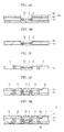
- FIG. 5A to FIG. 6I illustrate schematic cross sectional views of principal portions of individual manufacturing steps.
- the wiring conductor 24 adheres to the upper and lower surfaces of the first insulating layer 21 a in which the through hole 23 penetrating from the upper surface to the lower surface is formed, and inside the through hole 23 .
- the wiring conductor 24 is formed by, for example, a well-known semiadditive method or subtractive method.
- the cavity 22 is formed in the first insulating layer 21 a .
- the cavity 22 is formed by, for example, blasting or laser processing.
- the first insulating layer 21 a is placed on an adhesive sheet N.
- the electronic component D is inserted into the cavity 22 , and the electronic component D is placed on the adhesive sheet N which is exposed in the cavity 22 .
- the second insulating layer 21 b is laminated on an upper side of the first insulating layer 21 a .
- the second insulating layer 21 b is laminated on the upper side of the first insulating layer 21 a under a vacuum condition. With this arrangement, the second insulating layer 21 b can be brought into intimate contact with the first insulating layer 21 a firmly.
- the adhesive sheet N is peeled off.
- the first insulating layer 21 a is laminated on the upper surface of the second insulating layer 21 b . With this arrangement, the insulating board 21 is formed.
- the via hole 25 which exposes the electronic component D and the wiring conductor 24 on the first insulating layer 21 a from the surfaces of the second insulating layers 21 b , 21 b , is formed. Thereafter, the wiring conductor 24 adheres to the surface of the second insulating layer 21 b and inside the via hole 25 .
- the wiring board B is formed by adhering of the solder resist layer 26 including a first opening 26 a and a second opening 26 b which expose therein the wiring conductor 24 formed on the second insulating layers 21 b , 21 b.
- the adhesive sheet N and the first insulating layer 21 a are brought into intimate contact with each other firmly by an influence of a step for firmly bringing the second insulating layer 21 b into intimate contact with the upper side of the first insulating layer 21 a under the vacuum condition as described above.
- an adhesive of the adhesive sheet N may remain on the surface of the first insulating layer 21 a .
- a method of manufacturing a wiring board according to the present invention includes the steps of: preparing an insulating layer including a cavity formation region and a wiring formation region surrounding the cavity formation region, and a separable metallic foil formed of a first metallic foil and a second metallic foil which are brought into intimate contact with each other in a separable manner; allowing the separable metallic foil to adhere to at least a lower face side of the insulating layer with the first metallic foil as an adhering surface; forming a cavity in the cavity formation region by digging the insulating layer and the separable metallic foil from an upper surface side of the insulating layer to a depth that reaches the second metallic foil on the lower surface side of the insulating layer but does not penetrate the second metallic foil; injecting a fixing resin into the cavity; inserting an electronic component into the cavity into which the fixing resin is injected, and fixing the electronic component by curing the fixing resin; and peeling off the second metallic foil from an intimate contact surface with the first metallic foil.
- the cavity is formed by digging the insulating layer and the separable metallic foil to a depth that reaches the second metallic foil on the lower surface side of the insulating layer but does not penetrate the second metallic foil. Then, the electronic component is inserted into the cavity into which the fixing resin is injected, and the electronic component is fixed by curing the fixing resin. After the fixing resin is cured, the second metallic foil is peeled off from the intimate contact surface with the first metallic foil. In this way, the surface of the insulating layer is covered with the second metallic foil while the fixing resin is not cured. As a result, the fixing resin does not adhere to the surface of the insulating layer.
- FIG. 1 is a schematic cross sectional view illustrating a wiring board manufactured by a method of manufacturing according to one embodiment of the present invention.
- FIGS. 2A to 2F and FIGS. 3G to 3K are schematic cross sectional views of principal portions of individual steps for explaining the method of manufacturing according to one embodiment of the present invention.
- FIG. 4 is a schematic cross sectional view illustrating a wiring board manufactured by a conventional method of manufacturing.
- FIGS. 5A to 5F and FIGS. 6G to 6I are schematic cross sectional views of principal portions of individual steps for explaining a conventional method of manufacturing.
- the wiring board A includes an insulating board 1 , a wiring conductor 4 , a solder resist layer 6 formed on the insulating board 1 and the wiring conductor 4 , and an electronic component D accommodated in the insulating board 1 .
- the insulating board 1 includes a first insulating layer 1 a , and second insulating layer 1 b , 1 b laminated on upper and lower surfaces of the first insulating layer 1 a .
- the insulating board 1 includes a cavity formation region X and a wiring formation region Y that surrounds the cavity formation region X.
- a cavity 2 for accommodating therein the electronic component D is formed in the cavity formation region X.
- the electronic component D is accommodated in the cavity 2 while the electronic component D is fixed by a fixing resin J.
- a plurality of through-holes 3 are formed in the first insulating layer 1 a .
- the wiring conductor 4 adheres to the upper and lower surfaces of the first insulating layer 1 a and inside the through-hole 3 .
- the wiring conductors 4 , 4 on the upper and lower surfaces of the first insulating layer 1 a are electrically connected to each other via the through holes 3 .
- a plurality of via holes 5 are formed in the second insulating layer 1 b .
- the wiring conductor 4 also adheres to a surface of the second insulating layer 1 b and inside the via holes 5 .
- Apart of the wiring conductor 4 on the surface of the second insulating layer 1 b is electrically connected to the wiring conductors 4 , 4 on the upper and lower surfaces of the first insulating layer 1 a via the via holes 5 .
- a different part of the wiring conductor 4 on the surface of the second insulating layer 1 b is electrically connected to an electrode T of the electronic component D through the via holes 5 .
- a part of the wiring conductor 4 formed on the upper surface of the second insulating layer 1 b on an upper surface side is exposed in a first opening 6 a formed in the solder resist layer 6 , and forms a semiconductor element connecting pad 7 .
- the semiconductor element S is mounted on an upper surface of the wiring board A.
- a part of the wiring conductor 4 formed on the lower surface of the second insulating layer 1 b on a lower surface side is exposed in a second opening 6 b formed in the solder resist layer 6 , and forms an external connection pad 8 for connection to an external electric circuit board. Then, by connecting the external connection pad 8 and an electrode of the external electric circuit board to each other, the semiconductor element S is electrically connected to the external electric circuit board, and the semiconductor element S operates by transmitting a signal between the semiconductor element S and the external electric circuit board via the wiring conductor 4 and the electronic component D.
- the electronic component D includes, for example, a chip capacitor for stabilizing power supply to a semiconductor element S, and the like.
- FIGS. 2A to 3K illustrate schematic cross sectional views of principal portions of individual manufacturing steps.
- a portion identical with the portion of the wiring board A described with reference to FIG. 1 is identified with an identical reference numeral, and the detailed description thereof will be omitted.
- the first insulating layer 1 a is made of an electric insulating material including, for example, glass cloth impregnated with a thermosetting resin such as epoxy resin or bismaleimide triazine resin.
- a thickness of the first metallic foil M 1 is about 1 to 3 ⁇ m, and a thickness of the second metallic foil M 2 is about 18 to 35 ⁇ m.
- the separable metallic foil M can be obtained by firmly crimping the first metallic foil M 1 and the second metallic foil M 2 to each other, or bonding them together by an easily strippable adhesive.
- the separable metallic foil M is placed on each of upper and lower surfaces of the first insulating layer 1 a such that the first metallic foil M 1 is placed on a side of the first insulating layer 1 a (adhesion surface). Then, the separable metallic foil M adheres to each of the upper and lower surfaces of the first insulating layer 1 a by heating and pressurizing the separable metallic foil M.
- a blast resist R is formed on a surface of the separable metallic foil M on an upper side.
- the blast resist R is a resin film having resistance to blasting, and is formed by photolithographying a dry film containing urethane resin which has impact resilience, extends and has photosensitivity having heat resistance.
- the blast resist R includes an opening for exposing the separable metallic foil M in the cavity formation region X.
- the first insulating layer 1 a which is exposed in the opening of the blast resist R is dug from above by blasting, and the cavity 2 for accommodating the electronic component D is formed.
- the first insulating layer 1 a and the separable metallic foil M are dug to a depth that reaches the second metallic foil M 2 on a lower side of the first insulating layer 1 a , but does not penetrate second metallic foil M 2 .
- the reason why the thickness of the first metallic foil M 1 is made smaller than the thickness of the second metallic foil M 2 is that it is necessary to make the thickness smaller for forming the wiring conductor 4 using at least a part of the first metallic foil M 1 as will be described later, whereas it is possible that, unless the second metallic foil M 2 is made larger to a certain degree, the second metallic foil M 2 may be broken when it is peeled off and may not be peeled off well as will be described later.
- a depth of a depression formed in the second metallic foil M 2 is preferably about 10 ⁇ m. If the depth of the depression is larger than 10 ⁇ m, a contact area between the fixing resin J and the second metallic foil M 2 becomes larger. For this reason, there is a case where the second metallic foil M 2 is difficult to be peeled off in a step described later in which the second metallic foil M 2 is peeled from the first metallic foil M 1 .
- the blasting can be performed using particles such as alumina having a particle size of 10 to 30 ⁇ m as a projection material.
- the blast resist R is peeled off and removed from the separable metallic foil M.
- the electronic component D is inserted into the cavity 2 . Then, the electronic component D is fixed inside the cavity 2 by curing the fixing resin J. In doing so, the second metallic foil M 2 serves to cover and protect the first insulating layer 1 a so that the fixing resin J which has not been cured does not adhere thereto.
- the second metallic foil M 2 is peeled off and removed from an intimate contact interface between the second metallic foil M 2 and the first metallic foil M 1 .
- the through-hole 3 is formed in the first insulating layer 1 a .
- the wiring conductor 4 is formed on the surface of the first insulating layer 1 a and inside the through-hole 3 .
- the through-hole 3 has a diameter of about 50 to 300 ⁇ m, and is formed, for example, by drilling, laser processing, blasting, or the like.
- the wiring conductor 4 can be formed by a well-known semiadditive method.
- electroless plating is applied in the through-hole 3 , and the wiring conductor 4 may be formed by the electroless plating, and by adhering of electrolytic plating while the first metallic foil M 1 on the surface of the first insulating layer 1 a serves as a base metal.
- the second insulating layer 1 b is laminated on upper surfaces of the first insulating layer 1 a and the wiring conductor 4 by a well-known build-up process, and the via hole 5 is formed. Thereafter, the wiring conductor 4 is formed in the second insulating layer 1 b and the via hole 5 .
- a diameter of the via hole 5 is about 20 to 100 ⁇ m.
- the via hole 5 is formed, for example, by laser processing.
- the second insulating layer 1 b is made of an electric insulating material including, for example, glass cloth impregnated with a thermosetting resin such as epoxy resin or bismaleimide triazine resin.
- the wiring board A is formed by forming the solder resist layer 6 including the first opening 6 a on the surface of the second insulating layer 1 b on the upper side, and forming the solder resist layer 6 including the second opening 6 b on the surface of the second insulating layer 1 b on the lower side.
- the solder resist layer 6 is formed by coating or sticking, for example, a resin paste or a film on the second insulating layer 1 b and the wiring conductor 4 , and thermally curing it.
- the resin paste or the film is made of an electric insulating material including thermosetting resin such as epoxy resin or polyimide resin.
- the cavity 2 is formed by digging the first insulating layer 1 a and the separable metallic foil M to a depth that reaches the second metallic foil M 2 on a lower surface side of the first insulating layer 1 a but does not penetrate the second metallic foil M 2 .
- the electronic component D is fixed by injecting the fixing resin J into the cavity 2 , inserting the electronic component D into the cavity 2 into which the fixing resin J has been injected, and curing the fixing resin J.
- the second metallic foil M 2 is peeled off from an intimate contact surface with the first metallic foil M 1 .
- the surface of the first insulating layer 1 a is covered with the first metallic foil M 1 while the fixing resin J is not cured. Consequently, the fixing resin J does not adhere to the surface of the first insulating layer 1 a .
- the second insulating layer 1 b can be brought into intimate contact with the surface of the first insulating layer 1 a in a stable manner, and this makes it possible to provide a wiring board having high insulation reliability, in which insulation properties between wiring conductors 4 formed in the first and second insulating layers are excellent.
- the present invention is not restricted to the embodiment described above, but can by variously modified within the scope recited in the claims.
- the cavity 2 is formed by blasting in the embodiment described above, this may be formed by laser processing, rooter processing, or drilling.
Landscapes
- Engineering & Computer Science (AREA)
- Microelectronics & Electronic Packaging (AREA)
- Production Of Multi-Layered Print Wiring Board (AREA)
- Manufacturing & Machinery (AREA)
Abstract
Description
Claims (5)
Applications Claiming Priority (2)
| Application Number | Priority Date | Filing Date | Title |
|---|---|---|---|
| JP2013180767A JP2015050309A (en) | 2013-08-31 | 2013-08-31 | Wiring board manufacturing method |
| JP2013-180767 | 2013-08-31 |
Publications (2)
| Publication Number | Publication Date |
|---|---|
| US20150059170A1 US20150059170A1 (en) | 2015-03-05 |
| US9655248B2 true US9655248B2 (en) | 2017-05-16 |
Family
ID=52581164
Family Applications (1)
| Application Number | Title | Priority Date | Filing Date |
|---|---|---|---|
| US14/468,707 Expired - Fee Related US9655248B2 (en) | 2013-08-31 | 2014-08-26 | Method of manufacturing a wiring board |
Country Status (5)
| Country | Link |
|---|---|
| US (1) | US9655248B2 (en) |
| JP (1) | JP2015050309A (en) |
| KR (1) | KR20150026901A (en) |
| CN (1) | CN104427775A (en) |
| TW (1) | TW201524297A (en) |
Families Citing this family (7)
| Publication number | Priority date | Publication date | Assignee | Title |
|---|---|---|---|---|
| JP6423313B2 (en) * | 2015-05-26 | 2018-11-14 | 新光電気工業株式会社 | Electronic component built-in substrate, method for manufacturing the same, and electronic apparatus |
| JP6292216B2 (en) * | 2015-12-10 | 2018-03-14 | 日立金属株式会社 | Multilayer ceramic substrate manufacturing method and multilayer ceramic substrate |
| KR20200055432A (en) | 2018-11-13 | 2020-05-21 | 삼성전기주식회사 | Printed circuit board |
| JP7405591B2 (en) * | 2019-12-12 | 2023-12-26 | 株式会社伸光製作所 | Manufacturing method of printed wiring board |
| US12087698B2 (en) * | 2021-01-28 | 2024-09-10 | Hefei Xinsheng Optoelectronics Technology Co., Ltd. | Wiring substrate, array substrate and light emitting module having control regions arranged into control region rows and control region columns |
| KR20220135762A (en) * | 2021-03-31 | 2022-10-07 | 삼성전기주식회사 | Printed circuit board |
| KR102908329B1 (en) * | 2021-03-31 | 2026-01-05 | 삼성전기주식회사 | Printed circuit board |
Citations (3)
| Publication number | Priority date | Publication date | Assignee | Title |
|---|---|---|---|---|
| US20060291173A1 (en) | 2005-06-22 | 2006-12-28 | Samsung Electro-Mechanics Co., Ltd. | Printed circuit board with embedded electronic components |
| US20070269590A1 (en) * | 2006-05-22 | 2007-11-22 | Hitachi Cable, Ltd. | Electronic device substrate, electronic device and methods for making same |
| US20090301766A1 (en) * | 2008-06-04 | 2009-12-10 | Samsung Electro-Mechanics Co., Ltd. | Printed circuit board including electronic component embedded therein and method of manufacturing the same |
Family Cites Families (3)
| Publication number | Priority date | Publication date | Assignee | Title |
|---|---|---|---|---|
| FI117814B (en) * | 2004-06-15 | 2007-02-28 | Imbera Electronics Oy | Procedure for manufacturing an electronics module |
| KR100645643B1 (en) * | 2004-07-14 | 2006-11-15 | 삼성전기주식회사 | Manufacturing Method of Printed Circuit Board with Passive Device Chip |
| JP5395360B2 (en) * | 2008-02-25 | 2014-01-22 | 新光電気工業株式会社 | Manufacturing method of electronic component built-in substrate |
-
2013
- 2013-08-31 JP JP2013180767A patent/JP2015050309A/en active Pending
-
2014
- 2014-08-21 TW TW103128752A patent/TW201524297A/en unknown
- 2014-08-26 US US14/468,707 patent/US9655248B2/en not_active Expired - Fee Related
- 2014-08-27 CN CN201410429133.0A patent/CN104427775A/en active Pending
- 2014-08-27 KR KR20140112147A patent/KR20150026901A/en not_active Ceased
Patent Citations (4)
| Publication number | Priority date | Publication date | Assignee | Title |
|---|---|---|---|---|
| US20060291173A1 (en) | 2005-06-22 | 2006-12-28 | Samsung Electro-Mechanics Co., Ltd. | Printed circuit board with embedded electronic components |
| JP2007005768A (en) | 2005-06-22 | 2007-01-11 | Samsung Electro-Mechanics Co Ltd | Printed circuit board with built-in electronic components and manufacturing method thereof |
| US20070269590A1 (en) * | 2006-05-22 | 2007-11-22 | Hitachi Cable, Ltd. | Electronic device substrate, electronic device and methods for making same |
| US20090301766A1 (en) * | 2008-06-04 | 2009-12-10 | Samsung Electro-Mechanics Co., Ltd. | Printed circuit board including electronic component embedded therein and method of manufacturing the same |
Also Published As
| Publication number | Publication date |
|---|---|
| TW201524297A (en) | 2015-06-16 |
| JP2015050309A (en) | 2015-03-16 |
| CN104427775A (en) | 2015-03-18 |
| US20150059170A1 (en) | 2015-03-05 |
| KR20150026901A (en) | 2015-03-11 |
Similar Documents
| Publication | Publication Date | Title |
|---|---|---|
| US9655248B2 (en) | Method of manufacturing a wiring board | |
| KR101241544B1 (en) | The printed circuit board and the method for manufacturing the same | |
| US11812556B2 (en) | Printed circuit board and manufacturing method thereof | |
| US20130319740A1 (en) | Electronic component built-in substrate and method of manufacturing the same | |
| JPWO2010007704A1 (en) | Flex-rigid wiring board and electronic device | |
| CN105517344B (en) | Embedded circuit board and method of manufacturing same | |
| JP2001251056A (en) | Manufacturing method of printed wiring board | |
| CN102119588A (en) | Method for manufacturing module with built-in component, and module with built-in component | |
| KR20160032625A (en) | Printed circuit board and manufacturing method thereof | |
| KR20170067481A (en) | Printed circuit board, eletronic device package the same and method for manufacturing for printed circuit board | |
| KR20160090626A (en) | Printed circuit board having embedded electronic devices and method of manufacturing the same | |
| KR20090096809A (en) | Method for manufacturing printed circuit board embedded with semiconductor parts | |
| US20140209361A1 (en) | Wiring board and method for manufacturing the same | |
| JP5176676B2 (en) | Manufacturing method of component-embedded substrate | |
| KR20160079658A (en) | Method for manufacturing wiring board | |
| JPH03120892A (en) | Multilayer printed circuit board and manufacture thereof | |
| KR101109287B1 (en) | Electronic component embedded printed circuit board and manufacturing method | |
| KR20120032946A (en) | Printed circuit board and manufacturing method thereof | |
| KR20110062975A (en) | Printed circuit board and manufacturing method thereof | |
| JP6367902B2 (en) | Wiring board | |
| KR20110080865A (en) | Carrier for manufacturing printed circuit board, manufacturing method thereof and manufacturing method of printed circuit board using same | |
| KR20080043207A (en) | Active element embedded printed circuit board manufacturing method | |
| JP2016127133A (en) | Method of manufacturing wiring board | |
| JP2015144151A (en) | Wiring board manufacturing method |
Legal Events
| Date | Code | Title | Description |
|---|---|---|---|
| AS | Assignment |
Owner name: KYOCERA SLC TECHNOLOGIES CORPORATION, JAPAN Free format text: ASSIGNMENT OF ASSIGNORS INTEREST;ASSIGNOR:NARUMI, DAISUKE;REEL/FRAME:033610/0485 Effective date: 20140811 |
|
| AS | Assignment |
Owner name: KYOCERA CIRCUIT SOLUTIONS, INC., JAPAN Free format text: CHANGE OF NAME;ASSIGNOR:KYOCERA SLC TECHNOLOGIES CORPORATION;REEL/FRAME:036344/0749 Effective date: 20141001 |
|
| AS | Assignment |
Owner name: KYOCERA CORPORATION, JAPAN Free format text: CHANGE OF NAME;ASSIGNOR:KYOCERA CIRCUIT SOLUTIONS, INC.;REEL/FRAME:038806/0631 Effective date: 20160401 |
|
| STCF | Information on status: patent grant |
Free format text: PATENTED CASE |
|
| FEPP | Fee payment procedure |
Free format text: MAINTENANCE FEE REMINDER MAILED (ORIGINAL EVENT CODE: REM.); ENTITY STATUS OF PATENT OWNER: LARGE ENTITY |
|
| LAPS | Lapse for failure to pay maintenance fees |
Free format text: PATENT EXPIRED FOR FAILURE TO PAY MAINTENANCE FEES (ORIGINAL EVENT CODE: EXP.); ENTITY STATUS OF PATENT OWNER: LARGE ENTITY |
|
| STCH | Information on status: patent discontinuation |
Free format text: PATENT EXPIRED DUE TO NONPAYMENT OF MAINTENANCE FEES UNDER 37 CFR 1.362 |
|
| FP | Lapsed due to failure to pay maintenance fee |
Effective date: 20210516 |