US9530199B1 - Technique for measuring overlay between layers of a multilayer structure - Google Patents
Technique for measuring overlay between layers of a multilayer structure Download PDFInfo
- Publication number
- US9530199B1 US9530199B1 US14/798,283 US201514798283A US9530199B1 US 9530199 B1 US9530199 B1 US 9530199B1 US 201514798283 A US201514798283 A US 201514798283A US 9530199 B1 US9530199 B1 US 9530199B1
- Authority
- US
- United States
- Prior art keywords
- layers
- image
- expected
- multilayer structure
- images
- Prior art date
- Legal status (The legal status is an assumption and is not a legal conclusion. Google has not performed a legal analysis and makes no representation as to the accuracy of the status listed.)
- Active
Links
Images


Classifications
-
- G—PHYSICS
- G06—COMPUTING; CALCULATING OR COUNTING
- G06T—IMAGE DATA PROCESSING OR GENERATION, IN GENERAL
- G06T7/00—Image analysis
- G06T7/0002—Inspection of images, e.g. flaw detection
- G06T7/0004—Industrial image inspection
-
- G—PHYSICS
- G06—COMPUTING; CALCULATING OR COUNTING
- G06T—IMAGE DATA PROCESSING OR GENERATION, IN GENERAL
- G06T7/00—Image analysis
- G06T7/0002—Inspection of images, e.g. flaw detection
- G06T7/0004—Industrial image inspection
- G06T7/001—Industrial image inspection using an image reference approach
-
- G—PHYSICS
- G03—PHOTOGRAPHY; CINEMATOGRAPHY; ANALOGOUS TECHNIQUES USING WAVES OTHER THAN OPTICAL WAVES; ELECTROGRAPHY; HOLOGRAPHY
- G03F—PHOTOMECHANICAL PRODUCTION OF TEXTURED OR PATTERNED SURFACES, e.g. FOR PRINTING, FOR PROCESSING OF SEMICONDUCTOR DEVICES; MATERIALS THEREFOR; ORIGINALS THEREFOR; APPARATUS SPECIALLY ADAPTED THEREFOR
- G03F7/00—Photomechanical, e.g. photolithographic, production of textured or patterned surfaces, e.g. printing surfaces; Materials therefor, e.g. comprising photoresists; Apparatus specially adapted therefor
- G03F7/70—Microphotolithographic exposure; Apparatus therefor
- G03F7/70483—Information management; Active and passive control; Testing; Wafer monitoring, e.g. pattern monitoring
- G03F7/70605—Workpiece metrology
- G03F7/70616—Monitoring the printed patterns
- G03F7/70633—Overlay, i.e. relative alignment between patterns printed by separate exposures in different layers, or in the same layer in multiple exposures or stitching
-
- G—PHYSICS
- G03—PHOTOGRAPHY; CINEMATOGRAPHY; ANALOGOUS TECHNIQUES USING WAVES OTHER THAN OPTICAL WAVES; ELECTROGRAPHY; HOLOGRAPHY
- G03F—PHOTOMECHANICAL PRODUCTION OF TEXTURED OR PATTERNED SURFACES, e.g. FOR PRINTING, FOR PROCESSING OF SEMICONDUCTOR DEVICES; MATERIALS THEREFOR; ORIGINALS THEREFOR; APPARATUS SPECIALLY ADAPTED THEREFOR
- G03F1/00—Originals for photomechanical production of textured or patterned surfaces, e.g., masks, photo-masks, reticles; Mask blanks or pellicles therefor; Containers specially adapted therefor; Preparation thereof
- G03F1/38—Masks having auxiliary features, e.g. special coatings or marks for alignment or testing; Preparation thereof
- G03F1/44—Testing or measuring features, e.g. grid patterns, focus monitors, sawtooth scales or notched scales
-
- G—PHYSICS
- G03—PHOTOGRAPHY; CINEMATOGRAPHY; ANALOGOUS TECHNIQUES USING WAVES OTHER THAN OPTICAL WAVES; ELECTROGRAPHY; HOLOGRAPHY
- G03F—PHOTOMECHANICAL PRODUCTION OF TEXTURED OR PATTERNED SURFACES, e.g. FOR PRINTING, FOR PROCESSING OF SEMICONDUCTOR DEVICES; MATERIALS THEREFOR; ORIGINALS THEREFOR; APPARATUS SPECIALLY ADAPTED THEREFOR
- G03F7/00—Photomechanical, e.g. photolithographic, production of textured or patterned surfaces, e.g. printing surfaces; Materials therefor, e.g. comprising photoresists; Apparatus specially adapted therefor
- G03F7/004—Photosensitive materials
- G03F7/09—Photosensitive materials characterised by structural details, e.g. supports, auxiliary layers
- G03F7/11—Photosensitive materials characterised by structural details, e.g. supports, auxiliary layers having cover layers or intermediate layers, e.g. subbing layers
-
- G—PHYSICS
- G06—COMPUTING; CALCULATING OR COUNTING
- G06T—IMAGE DATA PROCESSING OR GENERATION, IN GENERAL
- G06T7/00—Image analysis
- G06T7/0002—Inspection of images, e.g. flaw detection
- G06T7/0004—Industrial image inspection
- G06T7/0006—Industrial image inspection using a design-rule based approach
-
- G06T7/0024—
-
- G06T7/0079—
-
- G—PHYSICS
- G06—COMPUTING; CALCULATING OR COUNTING
- G06T—IMAGE DATA PROCESSING OR GENERATION, IN GENERAL
- G06T7/00—Image analysis
- G06T7/10—Segmentation; Edge detection
-
- G—PHYSICS
- G06—COMPUTING; CALCULATING OR COUNTING
- G06T—IMAGE DATA PROCESSING OR GENERATION, IN GENERAL
- G06T7/00—Image analysis
- G06T7/10—Segmentation; Edge detection
- G06T7/11—Region-based segmentation
-
- G—PHYSICS
- G06—COMPUTING; CALCULATING OR COUNTING
- G06T—IMAGE DATA PROCESSING OR GENERATION, IN GENERAL
- G06T7/00—Image analysis
- G06T7/10—Segmentation; Edge detection
- G06T7/12—Edge-based segmentation
-
- G—PHYSICS
- G06—COMPUTING; CALCULATING OR COUNTING
- G06T—IMAGE DATA PROCESSING OR GENERATION, IN GENERAL
- G06T7/00—Image analysis
- G06T7/10—Segmentation; Edge detection
- G06T7/143—Segmentation; Edge detection involving probabilistic approaches, e.g. Markov random field [MRF] modelling
-
- G—PHYSICS
- G06—COMPUTING; CALCULATING OR COUNTING
- G06T—IMAGE DATA PROCESSING OR GENERATION, IN GENERAL
- G06T7/00—Image analysis
- G06T7/10—Segmentation; Edge detection
- G06T7/194—Segmentation; Edge detection involving foreground-background segmentation
-
- G—PHYSICS
- G06—COMPUTING; CALCULATING OR COUNTING
- G06T—IMAGE DATA PROCESSING OR GENERATION, IN GENERAL
- G06T7/00—Image analysis
- G06T7/30—Determination of transform parameters for the alignment of images, i.e. image registration
-
- G—PHYSICS
- G06—COMPUTING; CALCULATING OR COUNTING
- G06T—IMAGE DATA PROCESSING OR GENERATION, IN GENERAL
- G06T7/00—Image analysis
- G06T7/30—Determination of transform parameters for the alignment of images, i.e. image registration
- G06T7/33—Determination of transform parameters for the alignment of images, i.e. image registration using feature-based methods
- G06T7/337—Determination of transform parameters for the alignment of images, i.e. image registration using feature-based methods involving reference images or patches
-
- H—ELECTRICITY
- H01—ELECTRIC ELEMENTS
- H01L—SEMICONDUCTOR DEVICES NOT COVERED BY CLASS H10
- H01L21/00—Processes or apparatus adapted for the manufacture or treatment of semiconductor or solid state devices or of parts thereof
- H01L21/70—Manufacture or treatment of devices consisting of a plurality of solid state components formed in or on a common substrate or of parts thereof; Manufacture of integrated circuit devices or of parts thereof
- H01L21/71—Manufacture of specific parts of devices defined in group H01L21/70
- H01L21/768—Applying interconnections to be used for carrying current between separate components within a device comprising conductors and dielectrics
-
- G—PHYSICS
- G06—COMPUTING; CALCULATING OR COUNTING
- G06T—IMAGE DATA PROCESSING OR GENERATION, IN GENERAL
- G06T2207/00—Indexing scheme for image analysis or image enhancement
- G06T2207/10—Image acquisition modality
- G06T2207/10056—Microscopic image
- G06T2207/10061—Microscopic image from scanning electron microscope
-
- G—PHYSICS
- G06—COMPUTING; CALCULATING OR COUNTING
- G06T—IMAGE DATA PROCESSING OR GENERATION, IN GENERAL
- G06T2207/00—Indexing scheme for image analysis or image enhancement
- G06T2207/20—Special algorithmic details
- G06T2207/20112—Image segmentation details
- G06T2207/20116—Active contour; Active surface; Snakes
-
- G—PHYSICS
- G06—COMPUTING; CALCULATING OR COUNTING
- G06T—IMAGE DATA PROCESSING OR GENERATION, IN GENERAL
- G06T2207/00—Indexing scheme for image analysis or image enhancement
- G06T2207/30—Subject of image; Context of image processing
- G06T2207/30108—Industrial image inspection
- G06T2207/30148—Semiconductor; IC; Wafer
Definitions
- the present invention relates to a technique for determining overlay between layers of a multilayer structure by analyzing an image which represents such a structure.
- the invention relates to automated inspection of modern integrated circuits which constitute micro-miniature semiconductor structures with multiple layers produced by lithography. More specifically, the invention relates to overlay assessment techniques which require utilizing a Scanning Electron Microscope (SEM) for obtaining the representing image.
- SEM Scanning Electron Microscope
- SEMs scanning electron microscopes
- SEM images contain a wealth of detail, which must be properly interpreted in order to identify the structures appearing in each image, to distinguish the structures from other features and to estimate their relative coordinates.
- SEM Sccanning Electron Microscope used for exposing a 3D IC to a primary electron beam, collecting data on responsive electron beams or scattering electrons from multiple layers of the 3D IC and further reconstructing a combined SEM image of the multiple layers by applying computer processing to the collected data.
- Available image or Given image an image representing a real multilayer structure
- SEM-image an example of Available/Given image
- CD SEM Critical Dimensions Scanning Electron Microscope, which is applicable in a wide range of nodes having dimensions from about 3000 nm to about 7 nm.
- CD-SEM delivers High Resolution, High Throughput, High Sensitivity and High Repeatability by utilizing more sophisticated electron optics and advanced image processing.
- Expected image image of one or more specific details/features/structures to be constructed and/or to be found in a specific layer of a multilayered structure.
- the Expected image may be a design image, for example a CAD-image created by utilizing CAD (computer-aided design) tools for designing features of a specific layer.
- Expected image may be a design image, simulated so as to look closer to a real object after manufacturing thereof according to the design.
- Overlay vector characterizing pattern-to-pattern alignment of one layer of a multilayer structure with respect to another layer thereof.
- Registration maximum possible alignment of two or more images by recognition of their mutual positioning. For example, registration may be performed by achieving maximal possible overlapping between the images.
- Segmentation of available image labeling pixels of the available image to associate the pixels with different classes of features (objects, elements).
- the features may be located at different layers of the multilayer structure.
- Image segmentation is typically used to locate objects and boundaries (lines, curves, etc.) in images. More precisely, image segmentation is the process of assigning a label to every pixel in an image such that pixels with the same label share certain characteristics. For example, a specific label may indicate a specific layer of the structure.
- Segmentation of SEM-image labeling pixels of a SEM-image of a multilayer structure, in order to obtain a segmented image Segm(x,y) where similarly labeled pixels form segments.
- the Segmentation is a process of labeling pixels of the SEM image by assigning, to every pixel having coordinates(x,y), an index j being index of the layer to which this pixels belongs.
- the index j may accept values from the interval ⁇ 1 . . . N ⁇ where N is a number of layers of the multilayer structure.
- Maps of layers of an N-layer multilayer structure is a set of N binary images each having the size of the given image.
- Map of a specific layer is a binary image comprising features of that layer only, which are visible on the Given image (and consequently on the Segmented image), and which are represented on the Map by areas of pixels (segments) labeled with the label of that specific layer. It may be written down as follows:
- One of the objects of the invention is providing a more universal technique for analysis of an image representing a real multilayer structure in order to determine overlays between layers of the structure.
- a more specific object of the invention is providing an effective and accurate technique for overlay measurement in multilayer semiconductor structures. That object has been recognized by the Inventors as a long felt need for a centralized, global measurement of overlay in the modern semiconductor multilayer structures.
- a method for determining overlay between layers of a multilayer structure comprising
- the proposed method allows determining overlay for each layer of the multilayered structure, with respect to any of the remaining layers.
- overlay may be determined for all layers of the structure, in any combinations.
- expected images of the layers and/or the combined expected image may be understood as design images which have undergone simulation, for creating similarity thereof to the given image of the real multilayer structure (i.e., to imitate real appearance of the combined image/layers upon fabrication). Such expected images are called simulated design images.
- the method is a method of measuring overhead between layers of a multilayered semiconductor structure, wherein
- the segmentation may refer to the expected images of the layers, i.e. the method may comprise taking the expected images into account while performing the segmentation.
- the proposed technique may be improved by iteratively enhancing the segmentation, so as to more accurately distinguish features located on different layers or on the same layer, per pixel of the given image (SEM-image).
- Results of the segmentation may be corrected by adjusting the expected image(s) of the layer(s). It can be done based on the measured overlay.
- the segmentation results may be enhanced by using feedback about the measured overlay.
- a different technique intended for measuring overlay and using segmentation may also be improved by iteratively enhancing the segmentation based on results of the overlay measurements.
- the method may comprise correcting the segmentation results by:
- the overlay may be then measured again, based on the corrected segmentation, and the method may be continued iteratively.
- the mentioned feedback, and more specifically the step of correcting the expected image (CAD-image) of a layer may be caused, for example by a situation where the measured overlay does not exceed a predetermined limit of overlay and/or can be improved by shifting/adjusting CAD-image of the layer to be closer to the corresponding map (SEM-map) of the layer, thus improving the segmentation results on the next step of the process.
- CAD-image expected image
- SEM-map corresponding map
- the method may comprise as many iterations as allowed by a set of existing/predetermined limitations.
- the limitations may relate to time, quality and cost of the overlay measurement procedure, overlay value, etc. Some other limitations will be mentioned as the description proceeds.
- the method may comprise taking into account additional, probable occlusions which could be caused within one or more predetermined limits of acceptable offset.
- Such limits may be known in advance for manufacturing multilayer structures (such as semiconductor wafers) that satisfy specific quality requirements.
- One example of the discussed limits may be “CAD to SEM maximal variation” which limits acceptable changes of elements' sizes on a layer.
- Another example of the limits is “CAD to SEM maximal shift”, which limits acceptable overlay between specific layers. For example, elements of one transistor, which are deposited on different layers of the structure, will not form the properly operating transistor if overlays between these different layers and/or sizes of the elements vary over a set of some predetermined accepted limits Structures where the overlay exceeds the predetermined limit/s are usually considered as defective.
- CAD correction is performed (say, the layer's CAD image is shifted to become closer to the segmented image of the layer), the segmentation could be improved through more confident use of CAD information.
- the additional/probable occlusions may be taken into account at the step of segmentation and even thereafter, to define so called safe areas on the expected images of the layers and respectively on the maps of the layers, said safe areas being those associated with such segments of elements belonging to said layer, which segments would be visible on the given image despite the expected and the additional (probable) occlusions and distortions between the expected images and the given image.
- An example of such a distortion may be a CAD-SEM images deviation.
- the safe areas relate to segments of the elements, which remain visible i.e., cannot be occluded by any limited offset or distortion (maximal possible overlay, probable variations of sizes, etc.). It goes without saying that elements which are not occluded at all will be considered to form safe areas on the expected images and on the maps of the layers.
- the step of determining (measuring) of overlay between any two layers of the multilayer structure may be performed, for example, according to one of the following two versions.
- the method may comprise:
- the measurement of the shift may be presented as measuring of X/Y shift of the map (say, SEM map) of the specific layer along two axes X and Y with respect to the expected image (say, CAD-image) of said specific layer;
- per-layer registration may be performed more effectively if the registration is based on the safe areas described above.
- the method may comprise:
- V 1 is preferably estimated on the SEM image, while V 2 is estimated on the CAD image.
- the second option of the overlay measurement may be performed when only one of said two areas is MSA and/or only one of said two segments is ESA, while the other areas/segments are not the safe areas.
- the method is advantageous since it is adapted to perform measurement of overlay for any number of additionally selected alternative pairs of the layers, in other words—for all layers of the multilayer structure.
- the inventive method may alternatively be defined as follows:
- a method for performing determining overlay between layers of a multilayer structure comprising
- a method for determining overlay between layers of a multilayer structure comprising
- the method described above is advantageous for inspecting the multilayer structures such as modern semiconductor wafers or 3D IC, based on SEM-imaging of the structure and preliminarily designed images of the layers. Moreover, it easily allows measuring overlay values for all layers of the structure.
- the newly proposed method is effective for any structures and especially advantageous for 3C IC structures inspected using SEM, since it is
- a computer software product including a non-transitory computer-readable medium in which program instructions are stored, which instructions, when read by a computer, cause the computer to perform steps of the method described above.
- FIG. 1 schematically illustrates an embodiment of the system adapted to perform the inventive method for measuring overlay in a multilayer structure.
- the structure is a semiconductor wafer
- the initial (given) image is obtained by SEM and processed by a computer processor.
- FIG. 2 illustrates a schematic block diagram of one version of the proposed method.
- FIG. 3 illustrates a block diagram of another version of the proposed method, which comprises determining areas safe from occlusion on expected images of the layers and on their maps, which safe areas allow more effective segmentation and, consequently, more accurate measurement of overlay.
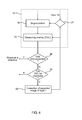
- FIG. 4 illustrates a block diagram of a further version of the proposed method, which comprises feedback that allows improving overlay at further steps of manufacturing/inspection based on the obtained measurements.
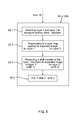
- FIG. 5 illustrates a block diagram of one exemplary process (using per layer registration) for measuring overlay between two selected layers of the multilayer structure.
- FIG. 6 illustrates a block diagram of another exemplary process (using COGs approach based on safe areas) for measuring overlay between two selected layers of the multilayer structure.
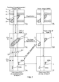
- FIG. 7 presents a schematic illustration of different stages of the proposed process by pictorial illustrations of: a combined expected image and a given image of a structure; an expected image and a map of one layer; stages of defining so-called safe areas.
- FIG. 8 is a schematic illustration of the exemplary process shown in FIG. 6 .
- FIG. 1 is a pictorial presentation of an exemplary set of equipment for implementing one embodiment of a system S according to the invention.
- the system S is intended for inspection of multilayer semiconductor structures (3D IC, wafers) using an electron scanning microscope SEM.
- the system S comprises a computer C with the processor (not shown) and the memory which is shown schematically as an external block M.
- the computer is also equipped with a display D and a keyboard K so that an operator may control and adjust the inspection process.
- the computer C is in communication, via line L, with the scanning electron microscope SEM which is adapted to create an image of a three-dimensional multilayer structure (a semiconductor wafer W is shown).
- the SEM-image obtained in the SEM is transmitted to the computer C, where it is processed and stored in the memory M.
- Memory M of the computer C also can store a set of expected images preliminarily developed for layers of the wafer W.
- Operation of the system S is focused on measuring overlay between layers of the wafer, based on processing the given image (SEM-image) and the expected images.
- the expected images may be CAD images designed for the layers.
- the expected images may be formed from the design images upon simulation, in order to make them looking maximally similar to real patterns on layers of the real structure of interest.
- the computer software may comprise one or more programs for simulation of the design images so as to convert them into expected images maximally close to images which could be obtained upon manufacturing the layers and scanning them by the SEM.
- the specific embodiment of the proposed system intended for measuring overlay in semiconductor wafers, operates more effectively with such a simulation.
- the computer accommodates some computer readable media which contains the proposed software product (schematically shown as a dotted contour SP) responsible for novel functions of the system.
- FIG. 2 shows a flow chart of one version of the proposed method.
- the version 10 may serve a basic one for some modifications of the method.
- Block 12 obtaining a given image of a real multilayer structure.
- the given image is a SEM-image generated by a scanning electron microscope.
- Block 14 obtaining expected images of layers of the multilayer structure.
- the expected images may be, for example, CAD images or simulated CAD images.
- the mentioned variations of the expected images are stored in the computer memory.
- the given image may be compared with the expected images, using the following operations.
- Block 16 indicates that the given image (SEM-image) is registered with respect of the combined expected image.
- Block 18 is responsible for Segmentation of the given image, namely:
- Box 18 . 1 denotes that a segmented image is obtained, which means that each pixel of the given image is “labeled” by a label indicating the layer to which the specific pixel is related.
- the segmented image is stored in the computer memory.
- Box 18 . 2 indicates that a plurality of layer maps (including the map of an exemplary layer “i”) are then formed from the segmented image and stored in the memory.
- the maps are SEM-maps of the respective layers.
- the segmentation process which is performed in boxes 18 . 1 and 18 . 2 may be assisted and facilitated by taking into account the suitable expected images received in block 14 (these optional arrows are not shown in FIG. 2 ).
- Block 20 is a block of overlay (OVL) measurement.
- OTL overlay
- the concept of measuring overlay proposed by Block 20 is the basis of a so-called global overlay measurement. Namely, OVL between any two layers in a multilayered structure can be measured by processing their expected images and their maps together. If in our specific example the expected images are CAD-images, overlay between any two selected layers can be measured by processing the CAD-images and the SEM-maps of the selected two layers.
- FIG. 3 shows a fragment of a flowchart, illustrating how an additional feature, namely so-called safe areas, may be determined and combined with the method shown in FIG. 2 .
- the safe areas are defined in a new Block 15 .
- Block 15 comprises defining safe areas for each layer “i”, first on the expected image of that layer (in our specific example, on the simulated CAD-image of the layer).
- the safe area should be understood as such an area of an element/feature of the specific layer, which area cannot be occluded by any limited offset.
- a safe area of a feature of a specific layer should remain visible (i.e. not occluded by features belonging to other layers) at maximal allowed deviations of the features' sizes and of X/Y overlay between layers. There are predetermined limits of those deviations. The deviation limits are schematically indicated by an arrow of data fed to the block 15 .
- the defined safe areas are usually smaller than the expected visual segments of the features, i.e. than those considered visible in the expected images of the layers.
- FIGS. 7 and 8 will further provide some pictorial illustrations of the safe areas' meaning.
- the expected images of the layers, with the defined safe areas ESA may be used for obtaining the combined expected image (block 14 . 3 , not shown in FIG. 3 ) and then for proper registration in box 16 .
- Each MSA may be defined by comparing a specific ESA with the map of the layer of interest.
- the safe areas determined on the expected images and maps of the layers are then used for accurate measurement of overlay between two selected layers. Due to that, the general Block 20 is modified in FIG. 3 and marked 20 A (since the OVL measurement is based on the safe areas.)
- FIG. 4 illustrates a flowchart of a modified method for overlay measurement, which comprises a feedback based on the measurement results.
- a method comprising the feedback may start with the flowchart 10 described with reference to FIG. 2 .
- the result is compared with a predetermined OVL limit (block 22 ). If the limit is exceeded, the product (such as a semiconductor wafer) is considered defective. The defective wafer may be discarded; alternatively, upper layer(s) of the structure may be removed and then deposited again.
- a predetermined OVL limit block 22
- the corrected expected image of a specific layer is then fed back to the Segmentation block 18 to improve results of Segmentation.
- the Segmentation will be then performed with reference to the updated expected image of that layer (at least in box 18 . 2 ).
- Box 27 receives information on the expected layer image from block 14 and block 26 , and will select there-between the most update information for feeding it to block 18 .
- Such updated information from block 26 will also be fed to block 20 which is responsible for measuring OVL. Owing to that, at the next round of fabrication, overhead will be re-calculated with reference to the corrected expected image of that specific layer.
- FIG. 5 illustrates one possible version of measuring overlay based on the general algorithm defined in block 20 ( FIG. 2 ), optionally using a modified version defined in block 20 A ( FIG. 3 ).
- General algorithm of block 20 schematically describes the combined processing of maps and expected images of any two selected layers, to measure overlay there-between.
- Block 20 A adds to Block 20 a possibility to perform the processing using so-called safe areas.
- FIG. 5 schematically illustrates a specified flowchart of OVL calculation, which comprises:
- Such a per-layer registration comprises aligning of the expected image (say, a CAD image or a simulated CAD image) of a specific layer against its map (SEM-map). The operation is performed for layer 1 and for layer 2 based on their respective CAD and SEM images. The per-layer registration may be facilitated, if performed based on safe areas preliminarily defined on the expected images (CAD-simulated images) and maps (SEM-images) of the layer.
- Box 20 . 6 comprises calculation of overlay (OVL) as a difference between the two shifts obtained at box 20 . 4 .
- FIG. 6 shows another version of measuring overlay (OVL) between any two layers of the multilayer structure.
- OTL measuring overlay
- Box 20 . 1 selecting two layers for the OVL measurement (the same as in FIG. 5 ).
- Box 20 . 3 calling, from the computer memory, the maps of the two selected layers (i.e., segmentation maps of the layers) and ensuring that the maps are arranged in their real mutual positions (as in the structure).
- Safety areas are identified on the layer maps. Let for example, safe area 1 (MSA 1 ) is identified on the layer map of layer 1 , and safe area 2 (MSA 2 ) on the map of layer 2 .
- Box 20 . 7 determining Centers of Gravity (COGs) for the identified safe areas, and measuring vector V 1 between the COGs of the two safe areas MSA 1 and MSA 2 .
- the vector V 1 will indicate a “visible overlay” between maps of the layers. In our example, vector V 1 is determined for the Segmentation maps of the layers.
- Box 20 . 9 is for obtaining from the computer memory two expected images of the layers 1 , 2 , and for placing these expected images in their designed mutual positions.
- V 2 is determined for the expected images being CAD-images of the layers.
- FIG. 7 comprises six parts 7 a - 7 f.
- Part 7 a is a combined expected image of a 4-layer structure, where features/elements of each layer are marked by digits 1-4. Each digit (1, 2, 3, 4) indicates the number of the layer where the feature is to be located according to the design.
- the expected image is a simulated design image.
- Part 7 b shows a schematic pictorial view of the given image (in this example, a SEM-image) of the real structure. Spots of the given image may be then segmented by referring to the expected image of Part 7 a.
- Part 7 c is an expected image of layer 3 , where the dark silhouette corresponds to the diagonal element located on layer 3 .
- a dashed contour around the diagonal element 3 shows its allowed size deviation (delta-3).
- Dashed vertical lines show limits of size deviation of a vertical element 4 which is located on layer 4 .
- the size deviation of the element 4 is marked as delta-4. In reality, element 4 partially occludes element 3 .
- OTL lim which schematically shows the limit of overlay between layer 3 and layer 4 .
- Part 7 d shows a segmentation map of layer 3 , obtained upon segmentation of the given image of Part 7 b .
- the map of layer 3 shows only the segments of layer 3 which are seen on the given image. This map of layer 3 may be used for performing registration with the expected image of layer 3 (Part 7 c ) for further measurement of overlay, for example between layer 3 and layer 4 .
- Part 7 e schematically shows how expected safe areas ESA may be defined on the expected image of layer 3 , if we are to determine mutual positions (overlay) between layers 3 and 4 .
- ESA of layer 3 are the areas which will remain visible in the worst case of offset i.e., when both the size deviations and the overlay concerning layers 3 , 4 take place.
- FIG. Part 7 f schematically shows safe areas MSA on the map of layer 3 , which, in the worst case, may correspond to the safe areas ESA on the expected image of that layer.
- FIG. 8 presents a pictorial illustration of how to measure overlay between two exemplary layers (layer 1 and layer 2 ), using the concept of safe areas. The relevant algorithm is generally described with reference to FIG. 6 .
- the left-hand portion “A” of FIG. 8 illustrates two expected images (CAD-images) of layers 1 and 2 in their expected position with respect to one another.
- the right-hand portion “B” shows two segmentation maps of the layers 1 and 2 , in their real position regarding one another.
- the darkened segments are safe areas of the element L 2 .
- the darkened segment of L 2 and the whole L 1 are mapped safe areas (MSA).
- MSA mapped safe areas
- ESA only the darkened segment of L 2 suitable to “B” and the whole L 1 are ESA.
- vector V 1 is determined for “B” (SEGM-maps of layers 1 , 2 ), as a difference between COGs of the two safe areas MSA located at two different layers 1 and 2 .
- vector V 2 is determined for “A” (CAD-images of layers 1 , 2 ), as a difference between COGs of the two safe areas ESA located on two different layers 1 and 2 .
Landscapes
- Engineering & Computer Science (AREA)
- Physics & Mathematics (AREA)
- General Physics & Mathematics (AREA)
- Theoretical Computer Science (AREA)
- Computer Vision & Pattern Recognition (AREA)
- Quality & Reliability (AREA)
- Software Systems (AREA)
- Probability & Statistics with Applications (AREA)
- Manufacturing & Machinery (AREA)
- Structural Engineering (AREA)
- Architecture (AREA)
- Power Engineering (AREA)
- Microelectronics & Electronic Packaging (AREA)
- Computer Hardware Design (AREA)
- Condensed Matter Physics & Semiconductors (AREA)
- Testing Or Measuring Of Semiconductors Or The Like (AREA)
- Exposure And Positioning Against Photoresist Photosensitive Materials (AREA)
- Image Analysis (AREA)
- Length-Measuring Devices Using Wave Or Particle Radiation (AREA)
Priority Applications (12)
| Application Number | Priority Date | Filing Date | Title |
|---|---|---|---|
| US14/798,283 US9530199B1 (en) | 2015-07-13 | 2015-07-13 | Technique for measuring overlay between layers of a multilayer structure |
| KR1020227009880A KR20220042493A (ko) | 2015-07-13 | 2016-07-06 | 다층 구조물의 층들 사이의 오버레이를 측정하기 위한 기법 |
| PCT/US2016/041195 WO2017011247A1 (en) | 2015-07-13 | 2016-07-06 | Technique for measuring overlay between layers of a multilayer structure |
| KR1020187004381A KR102380088B1 (ko) | 2015-07-13 | 2016-07-06 | 다층 구조물의 층들 사이의 오버레이를 측정하기 위한 기법 |
| CN201680047092.6A CN108027566B (zh) | 2015-07-13 | 2016-07-06 | 用于测量多层结构的层之间叠对的技术 |
| JP2018501205A JP6591035B2 (ja) | 2015-07-13 | 2016-07-06 | 多層構造体の層間のオーバレイを測定する技法 |
| CN201910808592.2A CN110647012B (zh) | 2015-07-13 | 2016-07-06 | 用于测量多层结构的层之间叠对的技术 |
| TW105121992A TWI604197B (zh) | 2015-07-13 | 2016-07-13 | 用於測量多層結構的層之間疊對的技術 |
| US15/390,663 US9916652B2 (en) | 2015-07-13 | 2016-12-26 | Technique for measuring overlay between layers of a multilayer structure |
| US15/918,570 US10354376B2 (en) | 2015-07-13 | 2018-03-12 | Technique for measuring overlay between layers of a multilayer structure |
| JP2019168038A JP6929330B2 (ja) | 2015-07-13 | 2019-09-17 | 多層構造体の層間のオーバレイを測定する技法 |
| JP2021130578A JP7265592B2 (ja) | 2015-07-13 | 2021-08-10 | 多層構造体の層間のオーバレイを測定する技法 |
Applications Claiming Priority (1)
| Application Number | Priority Date | Filing Date | Title |
|---|---|---|---|
| US14/798,283 US9530199B1 (en) | 2015-07-13 | 2015-07-13 | Technique for measuring overlay between layers of a multilayer structure |
Related Child Applications (1)
| Application Number | Title | Priority Date | Filing Date |
|---|---|---|---|
| US15/390,663 Continuation US9916652B2 (en) | 2015-07-13 | 2016-12-26 | Technique for measuring overlay between layers of a multilayer structure |
Publications (2)
| Publication Number | Publication Date |
|---|---|
| US9530199B1 true US9530199B1 (en) | 2016-12-27 |
| US20170018066A1 US20170018066A1 (en) | 2017-01-19 |
Family
ID=57590096
Family Applications (3)
| Application Number | Title | Priority Date | Filing Date |
|---|---|---|---|
| US14/798,283 Active US9530199B1 (en) | 2015-07-13 | 2015-07-13 | Technique for measuring overlay between layers of a multilayer structure |
| US15/390,663 Active US9916652B2 (en) | 2015-07-13 | 2016-12-26 | Technique for measuring overlay between layers of a multilayer structure |
| US15/918,570 Active US10354376B2 (en) | 2015-07-13 | 2018-03-12 | Technique for measuring overlay between layers of a multilayer structure |
Family Applications After (2)
| Application Number | Title | Priority Date | Filing Date |
|---|---|---|---|
| US15/390,663 Active US9916652B2 (en) | 2015-07-13 | 2016-12-26 | Technique for measuring overlay between layers of a multilayer structure |
| US15/918,570 Active US10354376B2 (en) | 2015-07-13 | 2018-03-12 | Technique for measuring overlay between layers of a multilayer structure |
Country Status (6)
| Country | Link |
|---|---|
| US (3) | US9530199B1 (ja) |
| JP (3) | JP6591035B2 (ja) |
| KR (2) | KR20220042493A (ja) |
| CN (2) | CN108027566B (ja) |
| TW (1) | TWI604197B (ja) |
| WO (1) | WO2017011247A1 (ja) |
Cited By (6)
| Publication number | Priority date | Publication date | Assignee | Title |
|---|---|---|---|---|
| US20170243343A1 (en) * | 2015-07-13 | 2017-08-24 | Applied Materials Israel Ltd. | Technique for measuring overlay between layers of a multilayer structure |
| US10381222B2 (en) * | 2017-08-03 | 2019-08-13 | Tokyo Electron Limited | Substrate treatment method, computer storage medium and substrate treatment system |
| US10578980B2 (en) * | 2016-12-23 | 2020-03-03 | Asml Netherlands B.V. | Method of determining a position of a feature |
| US10734294B2 (en) * | 2016-07-29 | 2020-08-04 | Taiwan Semiconductor Manufacturing Co., Ltd. | System and method for measuring and improving overlay using electronic microscopic imaging and digital processing |
| CN113139936A (zh) * | 2021-03-31 | 2021-07-20 | 武汉钢铁有限公司 | 一种图像分割处理方法及装置 |
| US11182892B2 (en) | 2019-09-16 | 2021-11-23 | Kla Corporation | Periodic semiconductor device misregistration metrology system and method |
Families Citing this family (7)
| Publication number | Priority date | Publication date | Assignee | Title |
|---|---|---|---|---|
| US10217232B2 (en) * | 2017-02-08 | 2019-02-26 | Toyota Motor Engineering & Manufacturing North America, Inc. | Systems and methods for locally aligning map data |
| KR102461648B1 (ko) | 2018-12-06 | 2022-10-31 | 삼성전자주식회사 | 반도체 패턴 검출 장치 |
| KR20220029748A (ko) | 2019-08-30 | 2022-03-08 | 주식회사 히타치하이테크 | 계측 시스템, 소정의 구조를 포함하는 반도체의 화상 계측을 행할 때 사용하는 학습 모델을 생성하는 방법, 및 컴퓨터에, 소정의 구조를 포함하는 반도체의 화상 계측을 행할 때 사용하는 학습 모델을 생성하는 처리를 실행시키기 위한 프로그램을 저장하는 기억 매체 |
| CN115104122A (zh) * | 2020-02-13 | 2022-09-23 | Asml荷兰有限公司 | 在多带电粒子束检查中根据检查图像的轮廓提取方法 |
| US11967058B2 (en) | 2020-06-24 | 2024-04-23 | Kla Corporation | Semiconductor overlay measurements using machine learning |
| US11637043B2 (en) * | 2020-11-03 | 2023-04-25 | Applied Materials, Inc. | Analyzing in-plane distortion |
| WO2023213534A1 (en) * | 2022-05-04 | 2023-11-09 | Asml Netherlands B.V. | Systems, methods, and software for multilayer metrology |
Citations (16)
| Publication number | Priority date | Publication date | Assignee | Title |
|---|---|---|---|---|
| US5694481A (en) * | 1995-04-12 | 1997-12-02 | Semiconductor Insights Inc. | Automated design analysis system for generating circuit schematics from high magnification images of an integrated circuit |
| US5877861A (en) * | 1997-11-14 | 1999-03-02 | International Business Machines Corporation | Method for overlay control system |
| US6218200B1 (en) * | 2000-07-14 | 2001-04-17 | Motorola, Inc. | Multi-layer registration control for photolithography processes |
| US20020144221A1 (en) * | 2001-03-29 | 2002-10-03 | Tomonobu Noda | Manufacturing process evaluation method for semiconductor device and pattern shape evaluation apparatus using the evaluation method |
| US20030021465A1 (en) * | 2000-08-30 | 2003-01-30 | Michael Adel | Overlay marks, methods of overlay mark design and methods of overlay measurements |
| US20050100802A1 (en) * | 2002-05-22 | 2005-05-12 | Neal Callan | Method for post-OPC multi layer overlay quality inspection |
| US7065737B2 (en) * | 2004-03-01 | 2006-06-20 | Advanced Micro Devices, Inc | Multi-layer overlay measurement and correction technique for IC manufacturing |
| US7381503B2 (en) * | 2000-12-08 | 2008-06-03 | Litel Instruments | Reference wafer calibration reticle |
| US20080183323A1 (en) | 2007-01-25 | 2008-07-31 | Ovadya Menadeva | System, method and computer program product for evaluating an actual structural element of an eletrical circuit |
| US20090240466A1 (en) | 2007-06-11 | 2009-09-24 | Applied Materials Israel, Ltd. | Method and system for evaluating an object that has a repetitive pattern |
| US20090238443A1 (en) * | 2008-03-18 | 2009-09-24 | Hidetoshi Sato | Pattern measurement methods and pattern measurement equipment |
| US7792351B1 (en) | 2006-05-25 | 2010-09-07 | Kla-Tencor Technologies Corporation | Defect review using image segmentation |
| US20110261264A1 (en) * | 2008-12-24 | 2011-10-27 | Baham Zafarifar | Image Processing |
| US8126255B2 (en) * | 2007-09-20 | 2012-02-28 | Kla-Tencor Corp. | Systems and methods for creating persistent data for a wafer and for using persistent data for inspection-related functions |
| US8138498B2 (en) * | 2000-08-30 | 2012-03-20 | Kla-Tencor Technologies Corporation | Apparatus and methods for determining overlay of structures having rotational or mirror symmetry |
| US9093458B2 (en) * | 2012-09-06 | 2015-07-28 | Kla-Tencor Corporation | Device correlated metrology (DCM) for OVL with embedded SEM structure overlay targets |
Family Cites Families (33)
| Publication number | Priority date | Publication date | Assignee | Title |
|---|---|---|---|---|
| US5600734A (en) * | 1991-10-04 | 1997-02-04 | Fujitsu Limited | Electron beam tester |
| US5650247A (en) * | 1989-03-16 | 1997-07-22 | Dai Nippon Printing Co., Ltd. | Preparation and reproduction of filters and preparation of filter photographic materials |
| KR970010666B1 (ko) * | 1993-12-27 | 1997-06-30 | 현대전자산업 주식회사 | 반도체 소자의 패턴 중첩오차 측정방법 |
| US5699282A (en) * | 1994-04-28 | 1997-12-16 | The United States Of America As Represented By The Secretary Of Commerce | Methods and test structures for measuring overlay in multilayer devices |
| US5710619A (en) * | 1995-10-31 | 1998-01-20 | Anvik Corporation | Large-area, scan-and-repeat, projection patterning system with unitary stage and magnification control capability |
| CA2260440C (en) * | 1998-01-28 | 2007-08-28 | Chipworks Inc. | Automatic focused ion beam imaging system and method |
| JP2000171230A (ja) | 1998-09-29 | 2000-06-23 | Toshiba Corp | 微小パタ―ン形状検査方法及びその装置 |
| US6612159B1 (en) * | 1999-08-26 | 2003-09-02 | Schlumberger Technologies, Inc. | Overlay registration error measurement made simultaneously for more than two semiconductor wafer layers |
| US6350548B1 (en) * | 2000-03-15 | 2002-02-26 | International Business Machines Corporation | Nested overlay measurement target |
| US6484060B1 (en) * | 2000-03-24 | 2002-11-19 | Micron Technology, Inc. | Layout for measurement of overlay error |
| EP1314198B1 (en) * | 2000-08-30 | 2017-03-08 | KLA-Tencor Corporation | Overlay marks, methods of overlay mark design and methods of overlay measurements |
| US6492073B1 (en) * | 2001-04-23 | 2002-12-10 | Taiwan Semiconductor Manufacturing Company | Removal of line end shortening in microlithography and mask set for removal |
| US7804994B2 (en) | 2002-02-15 | 2010-09-28 | Kla-Tencor Technologies Corporation | Overlay metrology and control method |
| KR100620199B1 (ko) * | 2002-04-15 | 2006-09-01 | 동부일렉트로닉스 주식회사 | 멀티 이미지를 사용한 오버레이 측정 방법 |
| DE10337767A1 (de) * | 2003-08-14 | 2005-03-31 | Leica Microsystems Semiconductor Gmbh | Verfahren zur Messung der Overlay-Verschiebung |
| JP4230980B2 (ja) * | 2004-10-21 | 2009-02-25 | 株式会社東芝 | パターンマッチング方法およびプログラム |
| CA2507174C (en) * | 2005-05-13 | 2013-07-16 | Semiconductor Insights Inc. | Method of registering and aligning multiple images |
| JP4988274B2 (ja) * | 2006-08-31 | 2012-08-01 | 株式会社日立ハイテクノロジーズ | パターンのずれ測定方法、及びパターン測定装置 |
| CN101436580B (zh) * | 2007-11-12 | 2010-11-17 | 财团法人工业技术研究院 | 叠对量测结构及方法 |
| NL2002932A1 (nl) * | 2008-06-02 | 2009-12-03 | Asml Netherlands Bv | Sub-wavelength segmentation in measurement targets on substrates. |
| CN101900945B (zh) * | 2009-05-27 | 2012-05-23 | 中芯国际集成电路制造(上海)有限公司 | 叠对误差补偿方法 |
| US8143731B2 (en) * | 2009-07-14 | 2012-03-27 | Nanya Technology Corp. | Integrated alignment and overlay mark |
| CN102163012B (zh) * | 2010-02-22 | 2013-01-09 | 索尔思光电股份有限公司 | 虚拟光罩系统及虚拟光罩叠合方法 |
| JP5639797B2 (ja) * | 2010-07-01 | 2014-12-10 | 株式会社日立ハイテクノロジーズ | パターンマッチング方法,画像処理装置、及びコンピュータプログラム |
| JP5501161B2 (ja) * | 2010-08-31 | 2014-05-21 | 株式会社日立ハイテクノロジーズ | 画像処理装置、及びコンピュータプログラム |
| JP5639925B2 (ja) * | 2011-02-25 | 2014-12-10 | 株式会社日立ハイテクノロジーズ | パターンマッチング装置、及びコンピュータープログラム |
| US9007585B2 (en) * | 2012-03-07 | 2015-04-14 | Kla-Tencor Corporation | Imaging overlay metrology target and complimentary overlay metrology measurement system |
| WO2014005828A1 (en) * | 2012-07-05 | 2014-01-09 | Asml Netherlands B.V. | Metrology for lithography |
| US9017926B2 (en) * | 2012-09-05 | 2015-04-28 | Nanya Technology Corporation | Overlay mark and method of forming the same |
| US20150321462A1 (en) * | 2013-04-26 | 2015-11-12 | Chemence, Inc. | Flexographic Printing Plates and Methods |
| JP2015049282A (ja) * | 2013-08-30 | 2015-03-16 | Hoya株式会社 | 表示装置製造用フォトマスク、該フォトマスクの製造方法、パターン転写方法及び表示装置の製造方法 |
| CN105225978B (zh) * | 2014-06-17 | 2019-06-04 | 联华电子股份有限公司 | 叠对误差的校正方法 |
| US9530199B1 (en) * | 2015-07-13 | 2016-12-27 | Applied Materials Israel Ltd | Technique for measuring overlay between layers of a multilayer structure |
-
2015
- 2015-07-13 US US14/798,283 patent/US9530199B1/en active Active
-
2016
- 2016-07-06 KR KR1020227009880A patent/KR20220042493A/ko not_active Application Discontinuation
- 2016-07-06 JP JP2018501205A patent/JP6591035B2/ja active Active
- 2016-07-06 CN CN201680047092.6A patent/CN108027566B/zh active Active
- 2016-07-06 WO PCT/US2016/041195 patent/WO2017011247A1/en active Application Filing
- 2016-07-06 CN CN201910808592.2A patent/CN110647012B/zh active Active
- 2016-07-06 KR KR1020187004381A patent/KR102380088B1/ko active IP Right Grant
- 2016-07-13 TW TW105121992A patent/TWI604197B/zh active
- 2016-12-26 US US15/390,663 patent/US9916652B2/en active Active
-
2018
- 2018-03-12 US US15/918,570 patent/US10354376B2/en active Active
-
2019
- 2019-09-17 JP JP2019168038A patent/JP6929330B2/ja active Active
-
2021
- 2021-08-10 JP JP2021130578A patent/JP7265592B2/ja active Active
Patent Citations (16)
| Publication number | Priority date | Publication date | Assignee | Title |
|---|---|---|---|---|
| US5694481A (en) * | 1995-04-12 | 1997-12-02 | Semiconductor Insights Inc. | Automated design analysis system for generating circuit schematics from high magnification images of an integrated circuit |
| US5877861A (en) * | 1997-11-14 | 1999-03-02 | International Business Machines Corporation | Method for overlay control system |
| US6218200B1 (en) * | 2000-07-14 | 2001-04-17 | Motorola, Inc. | Multi-layer registration control for photolithography processes |
| US20030021465A1 (en) * | 2000-08-30 | 2003-01-30 | Michael Adel | Overlay marks, methods of overlay mark design and methods of overlay measurements |
| US8138498B2 (en) * | 2000-08-30 | 2012-03-20 | Kla-Tencor Technologies Corporation | Apparatus and methods for determining overlay of structures having rotational or mirror symmetry |
| US7381503B2 (en) * | 2000-12-08 | 2008-06-03 | Litel Instruments | Reference wafer calibration reticle |
| US20020144221A1 (en) * | 2001-03-29 | 2002-10-03 | Tomonobu Noda | Manufacturing process evaluation method for semiconductor device and pattern shape evaluation apparatus using the evaluation method |
| US20050100802A1 (en) * | 2002-05-22 | 2005-05-12 | Neal Callan | Method for post-OPC multi layer overlay quality inspection |
| US7065737B2 (en) * | 2004-03-01 | 2006-06-20 | Advanced Micro Devices, Inc | Multi-layer overlay measurement and correction technique for IC manufacturing |
| US7792351B1 (en) | 2006-05-25 | 2010-09-07 | Kla-Tencor Technologies Corporation | Defect review using image segmentation |
| US20080183323A1 (en) | 2007-01-25 | 2008-07-31 | Ovadya Menadeva | System, method and computer program product for evaluating an actual structural element of an eletrical circuit |
| US20090240466A1 (en) | 2007-06-11 | 2009-09-24 | Applied Materials Israel, Ltd. | Method and system for evaluating an object that has a repetitive pattern |
| US8126255B2 (en) * | 2007-09-20 | 2012-02-28 | Kla-Tencor Corp. | Systems and methods for creating persistent data for a wafer and for using persistent data for inspection-related functions |
| US20090238443A1 (en) * | 2008-03-18 | 2009-09-24 | Hidetoshi Sato | Pattern measurement methods and pattern measurement equipment |
| US20110261264A1 (en) * | 2008-12-24 | 2011-10-27 | Baham Zafarifar | Image Processing |
| US9093458B2 (en) * | 2012-09-06 | 2015-07-28 | Kla-Tencor Corporation | Device correlated metrology (DCM) for OVL with embedded SEM structure overlay targets |
Non-Patent Citations (13)
| Title |
|---|
| Adel, M. et al., (Nov. 2007). The challenges of transitioning from linear to high-order overlay control in advanced lithography. In Photonics Asia 2007 (pp. 682722-682722). International Society for Optics and Photonics. 10 pages. |
| Ausschnitt, C.P. et al., (Mar. 2006). Multi-layer overlay metrology. In SPIE 31st International Symposium on Advanced Lithography (pp. 615210-615210). International Society for Optics and Photonics. 10 pages. |
| C.P. Ausschnitt et al, "Multi-Layer Overlay Metrology," Proc. SPIE 6152, 2006, 10 pages. |
| Dasari, P. et al., (Mar. 2010). A comparison of advanced overlay technologies. In SPIE Advanced Lithography (pp. 76381P-76381P). International Society for Optics and Photonics. 9 pages. |
| Eichelberger et al., "Overlay Control Requirements for Immersion Lithography," 2008 IEEE/SEMI Advanced Semiconductor Manufacturing Conference, 7 pages. |
| Eichelberger, B., et al., (May 2008). Overlay Control Requirements for Immersion Lithography. In 2008 IEEE/SEMI Advanced Semiconductor Manufacturing Conference (pp. 359-365). IEEE. 7 pages. |
| Englard I. et al., (Mar. 2008). Accurate in-resolution level overlay metrology for multipatterning lithography techniques. In SPIE Advanced Lithography (pp. 69221D-69221D). International Society for Optics and Photonics.,9 pages. |
| Felix, N. M. et al., (Mar. 2010). Smaller, smarter, faster, and more accurate: the new overlay metrology. In SPIE Advanced Lithography (pp. 76380Y-76380Y). International Society for Optics and Photonics. 7 pages. |
| Hotta, S., et al., (Mar. 2010). Concerning the influence of pattern symmetry on CD-SEM local overlay measurements for double patterning of complex shapes. In SPIE Advanced Lithography (pp. 76381T-76381T). International Society for Optics and Photonics. 13 pages. |
| International Roadmap Committee. (2013). International Technology Roadmap for Semiconductors: 2013 Edition Executive Summary. Semiconductor Industry Association, San Francisco, CA, available at: http://www. itrs. net/Links/2013ITRS/2013Chapters/2013ExecutiveSummary. pdf. 6 pages. |
| ITRS, "International Technology Roadmap for Semiconductors," 2013 edition Lithography Summary. Link to ITRS 2013 <http://itrs.net/ITRS%201999-2014%20Mtgs,%20Presentations%20&%20Links/2013ITRS/2013Chapters/2013Litho-Summary.pdf>, 6 pages. |
| R. M. Silver et al., "High Resolution Optical Overlay Metrology," Proceeding of SPIE vol. 5375 (SPIE, Bellingham, WA 2004), 18 pages. |
| Silver, R. M. et al., (May 2004). High-resolution optical overlay metrology. In Microlithography 2004 (pp. 78-95). International Society for Optics and Photonics. 18 pages. |
Cited By (10)
| Publication number | Priority date | Publication date | Assignee | Title |
|---|---|---|---|---|
| US20170243343A1 (en) * | 2015-07-13 | 2017-08-24 | Applied Materials Israel Ltd. | Technique for measuring overlay between layers of a multilayer structure |
| US9916652B2 (en) * | 2015-07-13 | 2018-03-13 | Applied Materials Israel Ltd. | Technique for measuring overlay between layers of a multilayer structure |
| US10354376B2 (en) * | 2015-07-13 | 2019-07-16 | Applied Materials Israel Ltd. | Technique for measuring overlay between layers of a multilayer structure |
| US10734294B2 (en) * | 2016-07-29 | 2020-08-04 | Taiwan Semiconductor Manufacturing Co., Ltd. | System and method for measuring and improving overlay using electronic microscopic imaging and digital processing |
| US10578980B2 (en) * | 2016-12-23 | 2020-03-03 | Asml Netherlands B.V. | Method of determining a position of a feature |
| US11392044B2 (en) | 2016-12-23 | 2022-07-19 | Asml Netherlands B.V. | Method of determining a position of a feature |
| US10381222B2 (en) * | 2017-08-03 | 2019-08-13 | Tokyo Electron Limited | Substrate treatment method, computer storage medium and substrate treatment system |
| US11182892B2 (en) | 2019-09-16 | 2021-11-23 | Kla Corporation | Periodic semiconductor device misregistration metrology system and method |
| CN113139936A (zh) * | 2021-03-31 | 2021-07-20 | 武汉钢铁有限公司 | 一种图像分割处理方法及装置 |
| CN113139936B (zh) * | 2021-03-31 | 2022-07-08 | 武汉钢铁有限公司 | 一种图像分割处理方法及装置 |
Also Published As
| Publication number | Publication date |
|---|---|
| CN110647012A (zh) | 2020-01-03 |
| JP2018522238A (ja) | 2018-08-09 |
| US10354376B2 (en) | 2019-07-16 |
| KR20220042493A (ko) | 2022-04-05 |
| US9916652B2 (en) | 2018-03-13 |
| JP6591035B2 (ja) | 2019-10-16 |
| JP6929330B2 (ja) | 2021-09-01 |
| TWI604197B (zh) | 2017-11-01 |
| CN110647012B (zh) | 2022-04-08 |
| JP7265592B2 (ja) | 2023-04-26 |
| JP2021185499A (ja) | 2021-12-09 |
| KR20180021206A (ko) | 2018-02-28 |
| CN108027566B (zh) | 2019-10-15 |
| WO2017011247A1 (en) | 2017-01-19 |
| KR102380088B1 (ko) | 2022-03-30 |
| US20170243343A1 (en) | 2017-08-24 |
| US20180268539A1 (en) | 2018-09-20 |
| CN108027566A (zh) | 2018-05-11 |
| US20170018066A1 (en) | 2017-01-19 |
| JP2020004443A (ja) | 2020-01-09 |
| TW201708823A (zh) | 2017-03-01 |
Similar Documents
| Publication | Publication Date | Title |
|---|---|---|
| US10354376B2 (en) | Technique for measuring overlay between layers of a multilayer structure | |
| US8867818B2 (en) | Method of creating template for matching, as well as device for creating template | |
| US9057873B2 (en) | Global alignment using multiple alignment pattern candidates | |
| US8767038B2 (en) | Method and device for synthesizing panorama image using scanning charged-particle microscope | |
| JP5948138B2 (ja) | 欠陥解析支援装置、欠陥解析支援装置で実行されるプログラム、および欠陥解析システム | |
| US20130010100A1 (en) | Image generating method and device using scanning charged particle microscope, sample observation method, and observing device | |
| US10545490B2 (en) | Method of inspecting a specimen and system thereof | |
| JP2016058637A (ja) | オーバーレイ計測方法、装置、および表示装置 | |
| JP2010085138A (ja) | 試料計測方法、及び計測装置 | |
| JP6713185B2 (ja) | テンプレートマッチングを用いた検査装置および検査方法 | |
| JP7390486B2 (ja) | 画像処理方法、形状検査方法、画像処理システム及び形状検査システム | |
| JP7273748B2 (ja) | 検査装置、検査方法、及びプログラム | |
| US10902620B1 (en) | Registration between an image of an object and a description | |
| CN114187294A (zh) | 基于先验信息的规则晶片定位方法 |
Legal Events
| Date | Code | Title | Description |
|---|---|---|---|
| AS | Assignment |
Owner name: APPLIED MATERIALS ISRAEL LTD., ISRAEL Free format text: ASSIGNMENT OF ASSIGNORS INTEREST;ASSIGNORS:WEINBERG, YAKOV;SCHWARZBAND, ISHAI;KRIS, ROMAN;AND OTHERS;SIGNING DATES FROM 20151102 TO 20151117;REEL/FRAME:037064/0531 |
|
| STCF | Information on status: patent grant |
Free format text: PATENTED CASE |
|
| MAFP | Maintenance fee payment |
Free format text: PAYMENT OF MAINTENANCE FEE, 4TH YEAR, LARGE ENTITY (ORIGINAL EVENT CODE: M1551); ENTITY STATUS OF PATENT OWNER: LARGE ENTITY Year of fee payment: 4 |