US9517530B2 - Wafer producing method - Google Patents
Wafer producing method Download PDFInfo
- Publication number
- US9517530B2 US9517530B2 US14/988,310 US201614988310A US9517530B2 US 9517530 B2 US9517530 B2 US 9517530B2 US 201614988310 A US201614988310 A US 201614988310A US 9517530 B2 US9517530 B2 US 9517530B2
- Authority
- US
- United States
- Prior art keywords
- ingot
- wafer
- laser beam
- modified layer
- plane
- Prior art date
- Legal status (The legal status is an assumption and is not a legal conclusion. Google has not performed a legal analysis and makes no representation as to the accuracy of the status listed.)
- Active
Links
- 238000000034 method Methods 0.000 title claims description 17
- 238000000926 separation method Methods 0.000 claims abstract description 30
- 239000013078 crystal Substances 0.000 claims abstract description 29
- 230000005540 biological transmission Effects 0.000 claims description 4
- 238000004519 manufacturing process Methods 0.000 claims description 3
- 239000010410 layer Substances 0.000 description 45
- 235000012431 wafers Nutrition 0.000 description 42
- 230000007246 mechanism Effects 0.000 description 12
- 238000003825 pressing Methods 0.000 description 9
- 238000005520 cutting process Methods 0.000 description 5
- 239000002346 layers by function Substances 0.000 description 4
- 230000001902 propagating effect Effects 0.000 description 4
- 230000015572 biosynthetic process Effects 0.000 description 3
- 238000000638 solvent extraction Methods 0.000 description 2
- 229910009372 YVO4 Inorganic materials 0.000 description 1
- 239000000853 adhesive Substances 0.000 description 1
- 230000001070 adhesive effect Effects 0.000 description 1
- 238000010586 diagram Methods 0.000 description 1
- 238000003384 imaging method Methods 0.000 description 1
- 230000006872 improvement Effects 0.000 description 1
- 238000012986 modification Methods 0.000 description 1
- 230000004048 modification Effects 0.000 description 1
- 230000003287 optical effect Effects 0.000 description 1
- 230000009467 reduction Effects 0.000 description 1
- 229910052710 silicon Inorganic materials 0.000 description 1
- 239000010703 silicon Substances 0.000 description 1
Images


Classifications
-
- B23K26/0057—
-
- H—ELECTRICITY
- H01—ELECTRIC ELEMENTS
- H01L—SEMICONDUCTOR DEVICES NOT COVERED BY CLASS H10
- H01L21/00—Processes or apparatus adapted for the manufacture or treatment of semiconductor or solid state devices or of parts thereof
- H01L21/02—Manufacture or treatment of semiconductor devices or of parts thereof
- H01L21/04—Manufacture or treatment of semiconductor devices or of parts thereof the devices having potential barriers, e.g. a PN junction, depletion layer or carrier concentration layer
- H01L21/18—Manufacture or treatment of semiconductor devices or of parts thereof the devices having potential barriers, e.g. a PN junction, depletion layer or carrier concentration layer the devices having semiconductor bodies comprising elements of Group IV of the Periodic Table or AIIIBV compounds with or without impurities, e.g. doping materials
- H01L21/30—Treatment of semiconductor bodies using processes or apparatus not provided for in groups H01L21/20 - H01L21/26
- H01L21/322—Treatment of semiconductor bodies using processes or apparatus not provided for in groups H01L21/20 - H01L21/26 to modify their internal properties, e.g. to produce internal imperfections
-
- B—PERFORMING OPERATIONS; TRANSPORTING
- B23—MACHINE TOOLS; METAL-WORKING NOT OTHERWISE PROVIDED FOR
- B23K—SOLDERING OR UNSOLDERING; WELDING; CLADDING OR PLATING BY SOLDERING OR WELDING; CUTTING BY APPLYING HEAT LOCALLY, e.g. FLAME CUTTING; WORKING BY LASER BEAM
- B23K26/00—Working by laser beam, e.g. welding, cutting or boring
- B23K26/0006—Working by laser beam, e.g. welding, cutting or boring taking account of the properties of the material involved
-
- B—PERFORMING OPERATIONS; TRANSPORTING
- B23—MACHINE TOOLS; METAL-WORKING NOT OTHERWISE PROVIDED FOR
- B23K—SOLDERING OR UNSOLDERING; WELDING; CLADDING OR PLATING BY SOLDERING OR WELDING; CUTTING BY APPLYING HEAT LOCALLY, e.g. FLAME CUTTING; WORKING BY LASER BEAM
- B23K26/00—Working by laser beam, e.g. welding, cutting or boring
- B23K26/50—Working by transmitting the laser beam through or within the workpiece
- B23K26/53—Working by transmitting the laser beam through or within the workpiece for modifying or reforming the material inside the workpiece, e.g. for producing break initiation cracks
-
- B—PERFORMING OPERATIONS; TRANSPORTING
- B28—WORKING CEMENT, CLAY, OR STONE
- B28D—WORKING STONE OR STONE-LIKE MATERIALS
- B28D5/00—Fine working of gems, jewels, crystals, e.g. of semiconductor material; apparatus or devices therefor
- B28D5/0005—Fine working of gems, jewels, crystals, e.g. of semiconductor material; apparatus or devices therefor by breaking, e.g. dicing
- B28D5/0011—Fine working of gems, jewels, crystals, e.g. of semiconductor material; apparatus or devices therefor by breaking, e.g. dicing with preliminary treatment, e.g. weakening by scoring
-
- C—CHEMISTRY; METALLURGY
- C30—CRYSTAL GROWTH
- C30B—SINGLE-CRYSTAL GROWTH; UNIDIRECTIONAL SOLIDIFICATION OF EUTECTIC MATERIAL OR UNIDIRECTIONAL DEMIXING OF EUTECTOID MATERIAL; REFINING BY ZONE-MELTING OF MATERIAL; PRODUCTION OF A HOMOGENEOUS POLYCRYSTALLINE MATERIAL WITH DEFINED STRUCTURE; SINGLE CRYSTALS OR HOMOGENEOUS POLYCRYSTALLINE MATERIAL WITH DEFINED STRUCTURE; AFTER-TREATMENT OF SINGLE CRYSTALS OR A HOMOGENEOUS POLYCRYSTALLINE MATERIAL WITH DEFINED STRUCTURE; APPARATUS THEREFOR
- C30B29/00—Single crystals or homogeneous polycrystalline material with defined structure characterised by the material or by their shape
- C30B29/10—Inorganic compounds or compositions
- C30B29/40—AIIIBV compounds wherein A is B, Al, Ga, In or Tl and B is N, P, As, Sb or Bi
- C30B29/403—AIII-nitrides
- C30B29/406—Gallium nitride
-
- H—ELECTRICITY
- H01—ELECTRIC ELEMENTS
- H01L—SEMICONDUCTOR DEVICES NOT COVERED BY CLASS H10
- H01L21/00—Processes or apparatus adapted for the manufacture or treatment of semiconductor or solid state devices or of parts thereof
- H01L21/02—Manufacture or treatment of semiconductor devices or of parts thereof
- H01L21/04—Manufacture or treatment of semiconductor devices or of parts thereof the devices having potential barriers, e.g. a PN junction, depletion layer or carrier concentration layer
- H01L21/18—Manufacture or treatment of semiconductor devices or of parts thereof the devices having potential barriers, e.g. a PN junction, depletion layer or carrier concentration layer the devices having semiconductor bodies comprising elements of Group IV of the Periodic Table or AIIIBV compounds with or without impurities, e.g. doping materials
- H01L21/30—Treatment of semiconductor bodies using processes or apparatus not provided for in groups H01L21/20 - H01L21/26
-
- B—PERFORMING OPERATIONS; TRANSPORTING
- B23—MACHINE TOOLS; METAL-WORKING NOT OTHERWISE PROVIDED FOR
- B23K—SOLDERING OR UNSOLDERING; WELDING; CLADDING OR PLATING BY SOLDERING OR WELDING; CUTTING BY APPLYING HEAT LOCALLY, e.g. FLAME CUTTING; WORKING BY LASER BEAM
- B23K2103/00—Materials to be soldered, welded or cut
- B23K2103/50—Inorganic material, e.g. metals, not provided for in B23K2103/02 – B23K2103/26
- B23K2103/56—Inorganic material, e.g. metals, not provided for in B23K2103/02 – B23K2103/26 semiconducting
-
- B23K2203/56—
Definitions
- the present invention relates to a wafer producing method for slicing a hexagonal single crystal ingot to produce a wafer.
- Various devices such as ICs and LSIs are formed by forming a functional layer on the front side of a wafer formed of silicon or the like and partitioning this functional layer into a plurality of regions along a plurality of crossing division lines.
- the division lines of the wafer are processed by a processing apparatus such as a cutting apparatus and a laser processing apparatus to thereby divide the wafer into a plurality of individual device chips corresponding to the respective devices.
- the device chips thus obtained are widely used in various equipment such as mobile phones and personal computers.
- power devices or optical devices such as LEDs and LDs are formed by forming a functional layer on the front side of a wafer formed of a hexagonal single crystal such as SiC and GaN and partitioning this functional layer into a plurality of regions along a plurality of crossing division lines.
- the wafer on which the devices are to be formed is produced by slicing an ingot with a wire saw. Both sides of the wafer obtained above are polished to a mirror finish (see Japanese Patent Laid-open No. 2000-94221, for example).
- This wire saw is configured in such a manner that a single wire such as a piano wire having a diameter of about 100 to 300 ⁇ m is wound around many grooves formed on usually two to four guide rollers to form a plurality of cutting portions spaced in parallel with a given pitch.
- the wire is operated to run in one direction or opposite directions, thereby slicing the ingot into a plurality of wafers.
- This technique includes the steps of setting the focal point of a laser beam having a transmission wavelength to SiC inside a hexagonal single crystal ingot, next applying the laser beam to the ingot as scanning the laser beam on the ingot to thereby form a modified layer and cracks in a separation plane inside the ingot, and next applying an external force to the ingot to thereby break the ingot along the separation plane where the modified layer and the cracks are formed, thus separating a wafer from the ingot.
- the laser beam is scanned spirally or linearly along the separation plane so that a first application point of the laser beam and a second application point of the laser beam nearest to the first application point have a predetermined positional relation with each other.
- the modified layer and the cracks are formed at very high density in the separation plane of the ingot.
- the laser beam is scanned spirally or linearly on the ingot.
- the direction of scanning of the laser beam is not specified.
- the pitch (spacing) between the first application point and the second application point of the laser beam as mentioned above is set to 1 to 10 ⁇ m. This pitch corresponds to the pitch of the cracks extending from the modified layer along a c-plane defined in the ingot.
- the pitch of the application points of the laser beam to be applied to the ingot is very small. Accordingly, regardless of whether the laser beam is scanned spirally or linearly, the laser beam must be applied with a very small pitch and the improvement in productivity is not yet sufficient.
- a wafer producing method for producing a hexagonal single crystal wafer from a hexagonal single crystal ingot having a first surface, a second surface opposite to the first surface, a c-axis extending from the first surface to the second surface, and a c-plane perpendicular to the c-axis, the wafer producing method including: a separation start point forming step of setting a focal point of a laser beam having a transmission wavelength to the ingot inside the ingot at a predetermined depth from the first surface, which depth corresponds to a thickness of the wafer to be produced, and next applying the laser beam to the first surface as relatively moving the focal point and the ingot to thereby form a modified layer parallel to the first surface and cracks extending from the modified layer along the c-plane, thus forming a separation start point; and a wafer separating step of separating a plate-shaped member having a thickness corresponding to the thickness of the wafer from the ingot at the separation
- the separation start point forming step includes: a modified layer forming step of relatively moving the focal point of the laser beam in a first direction perpendicular to a second direction where the c-axis is inclined by an off angle with respect to a normal to the first surface and the off angle is formed between the first surface and the c-plane, thereby linearly forming the modified layer extending in the first direction; and an indexing step of relatively moving the focal point in the second direction where the off angle is formed and the c-plane is inclined downward to thereby index the focal point by a predetermined amount.
- the focal point of the laser beam is relatively moved in the first direction perpendicular to the second direction where the off angle is formed between the first surface and the c-plane of the ingot, thereby linearly forming the modified layer extending in the first direction.
- the focal point of the laser beam is indexed by the predetermined amount in the second direction where the off angle is formed and the c-plane is inclined downward.
- the focal point of the laser beam is relatively moved again in the first direction to thereby linearly form the modified layer extending in the first direction.
- Such a series of steps are repeated to form a plurality of modified layers extending in the first direction.
- each linear modified layer is formed in the c-plane, and the cracks are also formed on both sides of each modified layer so as to propagate along the c-plane.
- the indexing direction as mentioned above, the application of the laser beam in the next path is not hindered by the cracks. Accordingly, the plate-shaped member having a thickness corresponding to the thickness of the wafer can be easily separated from the ingot at the separation start point, thereby producing the hexagonal single crystal wafer from the ingot.
- the scanning direction of the laser beam is set to the first direction perpendicular to the second direction where the off angle is formed. Accordingly, the cracks formed on both sides of each modified layer so as to propagate along the c-plane extend very long, so that the index amount of the focal point can be increased to thereby sufficiently improve the productivity. Further, the amount of the ingot to be discarded can be sufficiently reduced to about 30%.
- FIG. 1 is a perspective view of a laser processing apparatus suitable for use in performing a wafer producing method of the present invention
- FIG. 2 is a block diagram of a laser beam generating unit
- FIG. 3A is a perspective view of a hexagonal single crystal ingot
- FIG. 3B is an elevational view of the ingot shown in FIG. 3A ;
- FIG. 4 is a perspective view for illustrating a separation start point forming step
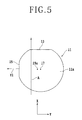
- FIG. 5 is a plan view of the ingot shown in FIG. 3A ;
- FIG. 6 is a schematic sectional view for illustrating a modified layer forming step
- FIG. 7 is a schematic plan view for illustrating the modified layer forming step
- FIG. 8A is a schematic plan view for illustrating an indexing step
- FIG. 8B is a schematic plan view for illustrating an index amount
- FIGS. 9A and 9B are perspective views for illustrating a wafer separating step
- FIG. 10 is a perspective view of a hexagonal single crystal wafer produced from the ingot.
- FIG. 11 is a schematic sectional view for illustrating the relation between the indexing direction of a laser beam to be applied and a c-plane of the ingot.
- FIG. 1 there is shown a perspective view of a laser processing apparatus 2 suitable for use in performing a wafer producing method of the present invention.
- the laser processing apparatus 2 includes a stationary base 4 and a first slide block 6 mounted on the stationary base 4 so as to be movable in the X direction.
- the first slide block 6 is moved in a feeding direction, or in the X direction along a pair of guide rails 14 by a feeding mechanism 12 composed of a ball screw 8 and a pulse motor 10 .
- a second slide block 16 is mounted on the first slide block 6 so as to be movable in the Y direction.
- the second slide block 16 is moved in an indexing direction, or in the Y direction along a pair of guide rails 24 by an indexing mechanism 22 composed of a ball screw 18 and a pulse motor 20 .
- a support table 26 is mounted on the second slide block 16 .
- the support table 26 is movable in the X direction and the Y direction by the feeding mechanism 12 and the indexing mechanism 22 and also rotatable by a motor stored in the second slide block 16 .
- a column 28 is provided on the stationary base 4 so as to project upward therefrom.
- a laser beam applying mechanism (laser beam applying means) 30 is mounted on the column 28 .
- the laser beam applying mechanism 30 is composed of a casing 32 , a laser beam generating unit 34 (see FIG. 2 ) stored in the casing 32 , and focusing means (laser head) 36 mounted on the front end of the casing 32 .
- An imaging unit 38 having a microscope and a camera is also mounted on the front end of the casing 32 so as to be aligned with the focusing means 36 in the X direction.
- the laser beam generating unit 34 includes a laser oscillator 40 for generating a pulsed laser beam such as YAG laser and YVO4 laser, repetition frequency setting means 42 for setting the repetition frequency of the pulsed laser beam to be generated from the laser oscillator 40 , pulse width adjusting means 44 for adjusting the pulse width of the pulsed laser beam to be generated from the laser oscillator 40 , and power adjusting means 46 for adjusting the power of the pulsed laser generated from the laser oscillator 40 .
- the laser oscillator 40 has a Brewster window, so that the laser beam generated from the laser oscillator 40 is a laser beam of linearly polarized light.
- the pulsed laser beam is reflected by a mirror 48 included in the focusing means 36 and next focused by a focusing lens 50 included in the focusing means 36 .
- the focusing lens 50 is positioned so that the pulsed laser beam is focused inside a hexagonal single crystal ingot 11 as a workpiece fixed to the support table 26 .
- FIG. 3A there is shown a perspective view of the hexagonal single crystal ingot 11 as a workpiece to be processed.
- FIG. 3B is an elevational view of the hexagonal single crystal ingot 11 shown in FIG. 3A .
- the hexagonal single crystal ingot (which will be hereinafter referred to also simply as ingot) 11 is selected from a SiC single crystal ingot or a GaN single crystal ingot.
- the ingot 11 has a first surface (upper surface) 11 a and a second surface (lower surface) 11 b opposite to the first surface 11 a .
- the first surface 11 a of the ingot 11 is preliminarily polished to a mirror finish because the laser beam is applied to the first surface 11 a.
- the ingot 11 has a first orientation flat 13 and a second orientation flat 15 perpendicular to the first orientation flat 13 .
- the length of the first orientation flat 13 is set greater than the length of the second orientation flat 15 .
- the ingot 11 has a c-axis 19 inclined by an off angle ⁇ toward the second orientation flat 15 with respect to a normal 17 to the upper surface 11 a and also has a c-plane 21 perpendicular to the c-axis 19 .
- the c-plane 21 is inclined by the off angle ⁇ with respect to the upper surface 11 a .
- the direction perpendicular to the direction of extension of the shorter second orientation flat 15 is the direction of inclination of the c-axis 19 .
- the c-plane 21 is set in the ingot 11 innumerably at the molecular level of the ingot 11 .
- the off angle ⁇ is set to 4°.
- the off angle ⁇ is not limited to 4° in the present invention.
- the off angle ⁇ may be freely set in the range of 1° to 6° in manufacturing the ingot 11 .
- a column 52 is fixed to the left side of the stationary base 4 .
- the column 52 is formed with a vertically elongated opening 53 , and a pressing mechanism 54 is vertically movably mounted to the column 52 so as to project from the opening 53 .
- the ingot 11 is fixed to the upper surface of the support table 26 by using a wax or adhesive in the condition where the second orientation flat 15 of the ingot 11 becomes parallel to the X direction.
- the direction of formation of the off angle ⁇ is shown by an arrow Y 1 . That is, the direction of the arrow Y 1 is the direction where the intersection 19 a between the c-axis 19 and the upper surface 11 a of the ingot 11 is present with respect to the normal 17 to the upper surface 11 a .
- the direction perpendicular to the direction of the arrow Y 1 is shown by an arrow A. Then, the ingot 11 is fixed to the support table 26 in the condition where the direction of the arrow A becomes parallel to the X direction.
- the laser beam is scanned in the direction of the arrow A perpendicular to the direction of the arrow Y 1 , or the direction of formation of the off angle ⁇ .
- the direction of the arrow A perpendicular to the direction of the arrow Y 1 where the off angle ⁇ is formed is defined as the feeding direction of the support table 26 .
- the scanning direction of the laser beam to be applied from the focusing means 36 is set to the direction of the arrow A perpendicular to the direction of the arrow Y 1 where the off angle ⁇ of the ingot 11 is formed. That is, it was found that by setting the scanning direction of the laser beam to the direction of the arrow A as mentioned above in the wafer producing method of the present invention, cracks propagating from a modified layer formed inside the ingot 11 by the laser beam extend very long along the c-plane 21 .
- a separation start point forming step is performed in such a manner that the focal point of the laser beam having a transmission wavelength (e.g., 1064 nm) to the hexagonal single crystal ingot 11 fixed to the support table 26 is set inside the ingot 11 at a predetermined depth from the first surface (upper surface) 11 a , which depth corresponds to the thickness of a wafer to be produced, and the laser beam is next applied to the upper surface 11 a as relatively moving the focal point and the ingot 11 to thereby form a modified layer 23 parallel to the upper surface 11 a and cracks 25 propagating from the modified layer 23 along the c-plane 21 , thus forming a separation start point (separation plane) where the modified layer 23 and the cracks 25 are formed.
- a transmission wavelength e.g. 1064 nm
- This separation start point forming step includes a modified layer forming step of relatively moving the focal point of the laser beam in the direction of the arrow A perpendicular to the direction of the arrow Y 1 where the c-axis 19 is inclined by the off angle ⁇ with respect to the normal 17 to the upper surface 11 a and the off angle ⁇ is formed between the c-plane 21 and the upper surface 11 a , thereby forming the modified layer 23 inside the ingot 11 and the cracks 25 propagating from the modified layer 23 along the c-plane 21 , and also includes an indexing step of relatively moving the focal point in the direction of formation of the off angle ⁇ , i.e., in the Y direction to thereby index the focal point by a predetermined amount as shown in FIG. 7 and FIGS. 8A and 8B .
- the modified layer 23 is linearly formed so as to extend in the X direction, so that the cracks 25 propagate from the modified layer 23 in opposite directions along the c-plane 21 .
- the separation start point forming step further includes an index amount setting step of measuring the width of the cracks 25 formed on one side of the modified layer 23 along the c-plane 21 and then setting the index amount of the focal point according to the width measured above. More specifically, letting W 1 denote the width of the cracks 25 formed on one side of the modified layer 23 so as to propagate from the modified layer 23 along the c-plane 21 , the index amount W 2 of the focal point is set in the range of W 1 to 2W 1 .
- the separation start point forming step is performed under the following laser processing conditions.
- NA of the focusing lens 0.45
- the width W 1 of the cracks 25 propagating from the modified layer 23 along the C-plane 21 in one direction as viewed in FIG. 6 is set to about 250 ⁇ m, and the index amount W 2 is set to 400 ⁇ m.
- the average power of the laser beam is not limited to 3.2 W.
- the width W 1 of the cracks 25 was about 100 ⁇ m.
- the width W 1 of the cracks 25 was about 350 ⁇ m.
- the average power of the laser beam to be applied is preferably set in the range of 2 to 4.5 W.
- the average power of the laser beam to be applied to the ingot 11 was set to 3.2 W in this preferred embodiment.
- the depth D 1 of the focal point from the upper surface 11 a in forming the modified layer 23 was set to 500 ⁇ m.
- FIG. 8A there is shown a schematic plan view for illustrating the scanning direction of the laser beam.
- the separation start point forming step is performed on a forward path X 1 and a backward path X 2 as shown in FIG. 8A . That is, the modified layer 23 is formed in the hexagonal single crystal ingot 11 on the forward path X 1 . Thereafter, the focal point of the laser beam is indexed by the predetermined amount. Thereafter, the modified layer 23 is formed again in the ingot 11 on the backward path X 2 .
- the index amount of the focal point of the laser beam is set in the range of W to 2W where W is the width of the cracks 25 formed on one side of the modified layer 23 along the c-plane 21
- the index amount of the focal point is preferably set to W or less until the modified layer 23 is first formed after setting the focal point of the laser beam inside the ingot 11 .
- the index amount of the focal point of the laser beam is 400 ⁇ m
- the index amount is set to 200 ⁇ m until the modified layer 23 is first formed inside the ingot 11 , and the laser beam is scanned plural times with this index amount of 200 ⁇ m as shown in FIG. 8B . That is, a first part of the plural scanning paths of the laser beam is idle, and when it is determined that the modified layer 23 has been first formed inside the ingot 11 , the index amount is set to 400 ⁇ m and the modified layer 23 is then formed inside the ingot 11 .
- the focal point of the laser beam is sequentially indexed to form a plurality of modified layers 23 at the depth D 1 in the whole area of the ingot 11 and also form the cracks 25 extending from each modified layer 23 along the c-plane 21 .
- a wafer separating step is performed in such a manner that an external force is applied to the ingot 11 to thereby separate a plate-shaped member having a thickness corresponding to the thickness of the wafer to be formed from the ingot 11 at the separation start point composed of the modified layers 23 and the cracks 25 , thus producing a hexagonal single crystal wafer 27 shown in FIG. 10 .
- This wafer separating step is performed by using the pressing mechanism 54 shown in FIG. 1 .
- the configuration of the pressing mechanism 54 is shown in FIGS. 9A and 9B .
- the pressing mechanism 54 includes a head 56 vertically movable by a moving mechanism (not shown) incorporated in the column 52 shown in FIG. 1 and a pressing member 58 rotatable in the direction shown by an arrow R in FIG. 9B with respect to the head 56 .
- the pressing mechanism 54 is relatively positioned above the ingot 11 fixed to the support table 26 .
- the head 56 is lowered until the pressing member 58 comes into pressure contact with the upper surface 11 a of the ingot 11 .
- the pressing member 58 In the condition where the pressing member 58 is in pressure contact with the upper surface 11 a of the ingot 11 , the pressing member 58 is rotated in the direction of the arrow R to thereby generate a torsional stress in the ingot 11 . As a result, the ingot 11 is broken at the separation start point where the modified layers 23 and the cracks 25 are formed. Accordingly, the hexagonal single crystal wafer 27 shown in FIG. 10 can be separated from the hexagonal single crystal ingot 11 . After separating the wafer 27 from the ingot 11 , the separation surface of the wafer 27 and the separation surface of the ingot 11 are preferably polished to a mirror finish.
- the c-plane 21 of the hexagonal single crystal ingot 11 in this preferred embodiment is inclined upward to the right as viewed in FIG. 3B by the off angle ⁇ with respect to the upper surface 11 a of the ingot 11 .
- the support table 26 holding the ingot 11 is moved in the direction shown by an arrow Y 1 in FIG. 11 to thereby index the focal point of the laser beam LB by the predetermined amount in the direction shown by an arrow Y 2 in FIG. 11 opposite to the arrow Y 1 , that is, in the direction where the off angle ⁇ is formed and the c-plane 21 is inclined downward.
- Each linear modified layer 23 is formed in the c-plane 21 , and the cracks 25 are also formed on both sides of each modified layer 23 so as to propagate along the c-plane 21 .
- the indexing direction as mentioned above, the application of the laser beam LB in the next path is not hindered by the cracks 25 . Accordingly, the plate-shaped member having a thickness corresponding to the thickness of the wafer can be easily separated from the ingot 11 at the separation start point, thereby producing the hexagonal single crystal wafer 27 from the ingot 11 .
Landscapes
- Engineering & Computer Science (AREA)
- Physics & Mathematics (AREA)
- Optics & Photonics (AREA)
- Chemical & Material Sciences (AREA)
- Mechanical Engineering (AREA)
- Plasma & Fusion (AREA)
- Chemical Kinetics & Catalysis (AREA)
- General Chemical & Material Sciences (AREA)
- Oil, Petroleum & Natural Gas (AREA)
- Condensed Matter Physics & Semiconductors (AREA)
- Manufacturing & Machinery (AREA)
- Power Engineering (AREA)
- Microelectronics & Electronic Packaging (AREA)
- Computer Hardware Design (AREA)
- General Physics & Mathematics (AREA)
- Crystallography & Structural Chemistry (AREA)
- Inorganic Chemistry (AREA)
- Organic Chemistry (AREA)
- Metallurgy (AREA)
- Materials Engineering (AREA)
- Mechanical Treatment Of Semiconductor (AREA)
- Laser Beam Processing (AREA)
- High Energy & Nuclear Physics (AREA)
- Processing Of Stones Or Stones Resemblance Materials (AREA)
- Electromagnetism (AREA)
- Health & Medical Sciences (AREA)
- Toxicology (AREA)
- Crystals, And After-Treatments Of Crystals (AREA)
Applications Claiming Priority (2)
| Application Number | Priority Date | Filing Date | Title |
|---|---|---|---|
| JP2015-001039 | 2015-01-06 | ||
| JP2015001039A JP6395613B2 (ja) | 2015-01-06 | 2015-01-06 | ウエーハの生成方法 |
Publications (2)
| Publication Number | Publication Date |
|---|---|
| US20160193690A1 US20160193690A1 (en) | 2016-07-07 |
| US9517530B2 true US9517530B2 (en) | 2016-12-13 |
Family
ID=56133278
Family Applications (1)
| Application Number | Title | Priority Date | Filing Date |
|---|---|---|---|
| US14/988,310 Active US9517530B2 (en) | 2015-01-06 | 2016-01-05 | Wafer producing method |
Country Status (8)
| Country | Link |
|---|---|
| US (1) | US9517530B2 (zh) |
| JP (1) | JP6395613B2 (zh) |
| KR (1) | KR102341602B1 (zh) |
| CN (1) | CN105750742B (zh) |
| DE (1) | DE102016200027B4 (zh) |
| MY (1) | MY180541A (zh) |
| SG (1) | SG10201510271QA (zh) |
| TW (1) | TWI673785B (zh) |
Cited By (20)
| Publication number | Priority date | Publication date | Assignee | Title |
|---|---|---|---|---|
| US20160158881A1 (en) * | 2014-12-04 | 2016-06-09 | Disco Corporation | Wafer producing method |
| US20160193691A1 (en) * | 2015-01-06 | 2016-07-07 | Disco Corporation | Wafer producing method |
| US20170015017A1 (en) * | 2015-07-16 | 2017-01-19 | Disco Corporation | Wafer producing method |
| US20170151627A1 (en) * | 2015-06-05 | 2017-06-01 | Disco Corporation | Wafer producing method |
| US9884390B2 (en) | 2014-12-04 | 2018-02-06 | Disco Corporation | Wafer producing method |
| US10076804B2 (en) | 2015-02-09 | 2018-09-18 | Disco Corporation | Wafer producing method |
| US10081076B2 (en) | 2015-04-06 | 2018-09-25 | Disco Corporation | Wafer producing method |
| US10297438B2 (en) | 2015-04-06 | 2019-05-21 | Disco Corporation | Water producing method |
| US10319593B2 (en) | 2015-07-21 | 2019-06-11 | Disco Corporation | Wafer thinning method |
| US10319594B2 (en) | 2015-07-21 | 2019-06-11 | Disco Corporation | Wafer thinning method |
| US10369659B2 (en) | 2015-02-09 | 2019-08-06 | Disco Corporation | Wafer producing method |
| US10406635B2 (en) | 2016-04-11 | 2019-09-10 | Disco Corporattion | Wafer producing method and processing feed direction detecting method |
| US10562130B1 (en) | 2018-12-29 | 2020-02-18 | Cree, Inc. | Laser-assisted method for parting crystalline material |
| US10573505B2 (en) * | 2017-01-31 | 2020-02-25 | Disco Corporation | SiC wafer producing method |
| US10576585B1 (en) | 2018-12-29 | 2020-03-03 | Cree, Inc. | Laser-assisted method for parting crystalline material |
| US10611052B1 (en) | 2019-05-17 | 2020-04-07 | Cree, Inc. | Silicon carbide wafers with relaxed positive bow and related methods |
| US10610973B2 (en) | 2015-06-02 | 2020-04-07 | Disco Corporation | Wafer producing method |
| US10625371B2 (en) | 2015-04-06 | 2020-04-21 | Disco Corporation | Wafer producing method |
| US10828726B2 (en) | 2017-02-16 | 2020-11-10 | Disco Corporation | SiC wafer producing method using ultrasonic wave |
| US11024501B2 (en) | 2018-12-29 | 2021-06-01 | Cree, Inc. | Carrier-assisted method for parting crystalline material along laser damage region |
Families Citing this family (10)
| Publication number | Priority date | Publication date | Assignee | Title |
|---|---|---|---|---|
| JP6698468B2 (ja) * | 2016-08-10 | 2020-05-27 | 株式会社ディスコ | ウエーハ生成方法 |
| JP6773506B2 (ja) * | 2016-09-29 | 2020-10-21 | 株式会社ディスコ | ウエーハ生成方法 |
| JP2018093046A (ja) * | 2016-12-02 | 2018-06-14 | 株式会社ディスコ | ウエーハ生成方法 |
| WO2018235843A1 (ja) | 2017-06-19 | 2018-12-27 | ローム株式会社 | 半導体装置の製造方法およびウエハ貼着構造体 |
| JP6896344B2 (ja) * | 2017-09-22 | 2021-06-30 | 株式会社ディスコ | チップの製造方法 |
| JP7096657B2 (ja) * | 2017-10-02 | 2022-07-06 | 株式会社ディスコ | ウェーハの加工方法 |
| JP7106217B2 (ja) | 2018-08-22 | 2022-07-26 | 株式会社ディスコ | ファセット領域の検出方法及び検出装置 |
| WO2020130054A1 (ja) * | 2018-12-21 | 2020-06-25 | 国立大学法人東海国立大学機構 | レーザ加工方法、半導体部材製造方法及びレーザ加工装置 |
| JP7479762B2 (ja) | 2020-08-03 | 2024-05-09 | 株式会社ディスコ | デバイスチップの製造方法 |
| JP2022050939A (ja) * | 2020-09-18 | 2022-03-31 | 株式会社ディスコ | ウエーハの生成方法 |
Citations (7)
| Publication number | Priority date | Publication date | Assignee | Title |
|---|---|---|---|---|
| US5912186A (en) * | 1995-11-21 | 1999-06-15 | Daido Hoxan, Inc. | Method for processing semiconductor material |
| JP2000094221A (ja) | 1998-09-24 | 2000-04-04 | Toyo Advanced Technologies Co Ltd | 放電式ワイヤソー |
| US20080070380A1 (en) | 2004-06-11 | 2008-03-20 | Showda Denko K.K. | Production Method of Compound Semiconductor Device Wafer |
| US7374955B2 (en) * | 2005-09-12 | 2008-05-20 | Covalent Materials Corporation | Method of manufacturing silicon wafer |
| US20090320897A1 (en) | 2008-06-26 | 2009-12-31 | Semiconductor Energy Laboratory Co., Ltd. | Photoelectric conversion device module and manufacturing method of the photoelectric conversion device module |
| JP2013049161A (ja) | 2011-08-30 | 2013-03-14 | Hamamatsu Photonics Kk | 加工対象物切断方法 |
| JP2013049461A (ja) | 2011-08-31 | 2013-03-14 | Fuji Seal International Inc | パウチ容器 |
Family Cites Families (11)
| Publication number | Priority date | Publication date | Assignee | Title |
|---|---|---|---|---|
| EP0152616A3 (en) * | 1983-12-23 | 1986-03-19 | International Paper Company | Method and apparatus to achieve raw edge protection |
| TWI520269B (zh) * | 2002-12-03 | 2016-02-01 | Hamamatsu Photonics Kk | Cutting method of semiconductor substrate |
| JP2009266892A (ja) * | 2008-04-22 | 2009-11-12 | Sumitomo Electric Ind Ltd | 化合物半導体結晶基材の製造方法 |
| JP5446325B2 (ja) | 2009-03-03 | 2014-03-19 | 豊田合成株式会社 | レーザ加工方法および化合物半導体発光素子の製造方法 |
| WO2012108052A1 (ja) * | 2011-02-10 | 2012-08-16 | 信越ポリマー株式会社 | 単結晶基板製造方法および内部改質層形成単結晶部材 |
| JP5875122B2 (ja) * | 2011-02-10 | 2016-03-02 | 信越ポリマー株式会社 | 単結晶基板製造方法および内部改質層形成単結晶部材 |
| JP2012238746A (ja) * | 2011-05-12 | 2012-12-06 | Disco Abrasive Syst Ltd | 光デバイスウエーハの分割方法 |
| JP2014041925A (ja) | 2012-08-22 | 2014-03-06 | Hamamatsu Photonics Kk | 加工対象物切断方法 |
| JP6026222B2 (ja) * | 2012-10-23 | 2016-11-16 | 株式会社ディスコ | ウエーハの加工方法 |
| JP5836998B2 (ja) * | 2013-04-23 | 2015-12-24 | 株式会社豊田中央研究所 | クラックの生成方法、レーザによる割断方法およびクラック生成装置 |
| JP6399914B2 (ja) * | 2014-12-04 | 2018-10-03 | 株式会社ディスコ | ウエーハの生成方法 |
-
2015
- 2015-01-06 JP JP2015001039A patent/JP6395613B2/ja active Active
- 2015-12-03 KR KR1020150171605A patent/KR102341602B1/ko active IP Right Grant
- 2015-12-08 TW TW104141116A patent/TWI673785B/zh active
- 2015-12-15 SG SG10201510271QA patent/SG10201510271QA/en unknown
- 2015-12-15 MY MYPI2015704561A patent/MY180541A/en unknown
- 2015-12-29 CN CN201511009172.6A patent/CN105750742B/zh active Active
-
2016
- 2016-01-05 DE DE102016200027.6A patent/DE102016200027B4/de active Active
- 2016-01-05 US US14/988,310 patent/US9517530B2/en active Active
Patent Citations (7)
| Publication number | Priority date | Publication date | Assignee | Title |
|---|---|---|---|---|
| US5912186A (en) * | 1995-11-21 | 1999-06-15 | Daido Hoxan, Inc. | Method for processing semiconductor material |
| JP2000094221A (ja) | 1998-09-24 | 2000-04-04 | Toyo Advanced Technologies Co Ltd | 放電式ワイヤソー |
| US20080070380A1 (en) | 2004-06-11 | 2008-03-20 | Showda Denko K.K. | Production Method of Compound Semiconductor Device Wafer |
| US7374955B2 (en) * | 2005-09-12 | 2008-05-20 | Covalent Materials Corporation | Method of manufacturing silicon wafer |
| US20090320897A1 (en) | 2008-06-26 | 2009-12-31 | Semiconductor Energy Laboratory Co., Ltd. | Photoelectric conversion device module and manufacturing method of the photoelectric conversion device module |
| JP2013049161A (ja) | 2011-08-30 | 2013-03-14 | Hamamatsu Photonics Kk | 加工対象物切断方法 |
| JP2013049461A (ja) | 2011-08-31 | 2013-03-14 | Fuji Seal International Inc | パウチ容器 |
Cited By (30)
| Publication number | Priority date | Publication date | Assignee | Title |
|---|---|---|---|---|
| US20160158881A1 (en) * | 2014-12-04 | 2016-06-09 | Disco Corporation | Wafer producing method |
| US9789565B2 (en) * | 2014-12-04 | 2017-10-17 | Disco Corporation | Wafer producing method |
| US9884390B2 (en) | 2014-12-04 | 2018-02-06 | Disco Corporation | Wafer producing method |
| US20160193691A1 (en) * | 2015-01-06 | 2016-07-07 | Disco Corporation | Wafer producing method |
| US9925619B2 (en) * | 2015-01-06 | 2018-03-27 | Disco Corporation | Wafer producing method |
| US10076804B2 (en) | 2015-02-09 | 2018-09-18 | Disco Corporation | Wafer producing method |
| US10369659B2 (en) | 2015-02-09 | 2019-08-06 | Disco Corporation | Wafer producing method |
| US10625371B2 (en) | 2015-04-06 | 2020-04-21 | Disco Corporation | Wafer producing method |
| US10081076B2 (en) | 2015-04-06 | 2018-09-25 | Disco Corporation | Wafer producing method |
| US10297438B2 (en) | 2015-04-06 | 2019-05-21 | Disco Corporation | Water producing method |
| US10610973B2 (en) | 2015-06-02 | 2020-04-07 | Disco Corporation | Wafer producing method |
| US9981339B2 (en) * | 2015-06-05 | 2018-05-29 | Disco Corporation | Wafer producing method |
| US20170151627A1 (en) * | 2015-06-05 | 2017-06-01 | Disco Corporation | Wafer producing method |
| US10029383B2 (en) * | 2015-07-16 | 2018-07-24 | Disco Corporation | Wafer producing method |
| US20170015017A1 (en) * | 2015-07-16 | 2017-01-19 | Disco Corporation | Wafer producing method |
| US10319593B2 (en) | 2015-07-21 | 2019-06-11 | Disco Corporation | Wafer thinning method |
| US10319594B2 (en) | 2015-07-21 | 2019-06-11 | Disco Corporation | Wafer thinning method |
| US10406635B2 (en) | 2016-04-11 | 2019-09-10 | Disco Corporattion | Wafer producing method and processing feed direction detecting method |
| US10573505B2 (en) * | 2017-01-31 | 2020-02-25 | Disco Corporation | SiC wafer producing method |
| US10828726B2 (en) | 2017-02-16 | 2020-11-10 | Disco Corporation | SiC wafer producing method using ultrasonic wave |
| US10576585B1 (en) | 2018-12-29 | 2020-03-03 | Cree, Inc. | Laser-assisted method for parting crystalline material |
| US10562130B1 (en) | 2018-12-29 | 2020-02-18 | Cree, Inc. | Laser-assisted method for parting crystalline material |
| US11024501B2 (en) | 2018-12-29 | 2021-06-01 | Cree, Inc. | Carrier-assisted method for parting crystalline material along laser damage region |
| US11219966B1 (en) | 2018-12-29 | 2022-01-11 | Wolfspeed, Inc. | Laser-assisted method for parting crystalline material |
| US11826846B2 (en) | 2018-12-29 | 2023-11-28 | Wolfspeed, Inc. | Laser-assisted method for parting crystalline material |
| US11901181B2 (en) | 2018-12-29 | 2024-02-13 | Wolfspeed, Inc. | Carrier-assisted method for parting crystalline material along laser damage region |
| US11911842B2 (en) | 2018-12-29 | 2024-02-27 | Wolfspeed, Inc. | Laser-assisted method for parting crystalline material |
| US10611052B1 (en) | 2019-05-17 | 2020-04-07 | Cree, Inc. | Silicon carbide wafers with relaxed positive bow and related methods |
| US11034056B2 (en) | 2019-05-17 | 2021-06-15 | Cree, Inc. | Silicon carbide wafers with relaxed positive bow and related methods |
| US11654596B2 (en) | 2019-05-17 | 2023-05-23 | Wolfspeed, Inc. | Silicon carbide wafers with relaxed positive bow and related methods |
Also Published As
| Publication number | Publication date |
|---|---|
| CN105750742A (zh) | 2016-07-13 |
| CN105750742B (zh) | 2019-11-29 |
| MY180541A (en) | 2020-12-01 |
| US20160193690A1 (en) | 2016-07-07 |
| SG10201510271QA (en) | 2016-08-30 |
| JP2016127186A (ja) | 2016-07-11 |
| JP6395613B2 (ja) | 2018-09-26 |
| KR102341602B1 (ko) | 2021-12-22 |
| KR20160084799A (ko) | 2016-07-14 |
| TW201635364A (zh) | 2016-10-01 |
| DE102016200027A1 (de) | 2016-07-07 |
| DE102016200027B4 (de) | 2023-04-27 |
| TWI673785B (zh) | 2019-10-01 |
Similar Documents
| Publication | Publication Date | Title |
|---|---|---|
| US9517530B2 (en) | Wafer producing method | |
| US9884390B2 (en) | Wafer producing method | |
| US9789565B2 (en) | Wafer producing method | |
| US10610973B2 (en) | Wafer producing method | |
| US10297438B2 (en) | Water producing method | |
| US10369659B2 (en) | Wafer producing method | |
| US9481051B2 (en) | Wafer producing method | |
| US10029383B2 (en) | Wafer producing method | |
| US9925619B2 (en) | Wafer producing method | |
| US9878397B2 (en) | SiC wafer producing method | |
| US10076804B2 (en) | Wafer producing method | |
| US9815138B2 (en) | Wafer producing method | |
| US9764428B2 (en) | Wafer producing method | |
| US9868177B2 (en) | Wafer producing method | |
| US10625371B2 (en) | Wafer producing method | |
| US9764420B2 (en) | Wafer producing method | |
| US10081076B2 (en) | Wafer producing method | |
| US10094047B2 (en) | Wafer producing method | |
| JP6366485B2 (ja) | ウエーハの生成方法 |
Legal Events
| Date | Code | Title | Description |
|---|---|---|---|
| AS | Assignment |
Owner name: DISCO CORPORATION, JAPAN Free format text: ASSIGNMENT OF ASSIGNORS INTEREST;ASSIGNORS:HIRATA, KAZUYA;TAKAHASHI, KUNIMITSU;NISHINO, YOKO;REEL/FRAME:037412/0416 Effective date: 20151215 |
|
| STCF | Information on status: patent grant |
Free format text: PATENTED CASE |
|
| MAFP | Maintenance fee payment |
Free format text: PAYMENT OF MAINTENANCE FEE, 4TH YEAR, LARGE ENTITY (ORIGINAL EVENT CODE: M1551); ENTITY STATUS OF PATENT OWNER: LARGE ENTITY Year of fee payment: 4 |