US9515286B2 - Laser welding transparent glass sheets using low melting glass or thin absorbing films - Google Patents
Laser welding transparent glass sheets using low melting glass or thin absorbing films Download PDFInfo
- Publication number
- US9515286B2 US9515286B2 US14/271,797 US201414271797A US9515286B2 US 9515286 B2 US9515286 B2 US 9515286B2 US 201414271797 A US201414271797 A US 201414271797A US 9515286 B2 US9515286 B2 US 9515286B2
- Authority
- US
- United States
- Prior art keywords
- substrate
- glass
- substrates
- laser
- inorganic film
- Prior art date
- Legal status (The legal status is an assumption and is not a legal conclusion. Google has not performed a legal analysis and makes no representation as to the accuracy of the status listed.)
- Active, expires
Links
Images


Classifications
-
- H—ELECTRICITY
- H10—SEMICONDUCTOR DEVICES; ELECTRIC SOLID-STATE DEVICES NOT OTHERWISE PROVIDED FOR
- H10K—ORGANIC ELECTRIC SOLID-STATE DEVICES
- H10K50/00—Organic light-emitting devices
- H10K50/80—Constructional details
- H10K50/84—Passivation; Containers; Encapsulations
- H10K50/842—Containers
- H10K50/8426—Peripheral sealing arrangements, e.g. adhesives, sealants
-
- H01L51/5246—
-
- B—PERFORMING OPERATIONS; TRANSPORTING
- B23—MACHINE TOOLS; METAL-WORKING NOT OTHERWISE PROVIDED FOR
- B23K—SOLDERING OR UNSOLDERING; WELDING; CLADDING OR PLATING BY SOLDERING OR WELDING; CUTTING BY APPLYING HEAT LOCALLY, e.g. FLAME CUTTING; WORKING BY LASER BEAM
- B23K26/00—Working by laser beam, e.g. welding, cutting or boring
- B23K26/20—Bonding
- B23K26/206—Laser sealing
-
- B—PERFORMING OPERATIONS; TRANSPORTING
- B32—LAYERED PRODUCTS
- B32B—LAYERED PRODUCTS, i.e. PRODUCTS BUILT-UP OF STRATA OF FLAT OR NON-FLAT, e.g. CELLULAR OR HONEYCOMB, FORM
- B32B17/00—Layered products essentially comprising sheet glass, or glass, slag, or like fibres
- B32B17/06—Layered products essentially comprising sheet glass, or glass, slag, or like fibres comprising glass as the main or only constituent of a layer, next to another layer of a specific material
-
- B—PERFORMING OPERATIONS; TRANSPORTING
- B32—LAYERED PRODUCTS
- B32B—LAYERED PRODUCTS, i.e. PRODUCTS BUILT-UP OF STRATA OF FLAT OR NON-FLAT, e.g. CELLULAR OR HONEYCOMB, FORM
- B32B37/00—Methods or apparatus for laminating, e.g. by curing or by ultrasonic bonding
- B32B37/06—Methods or apparatus for laminating, e.g. by curing or by ultrasonic bonding characterised by the heating method
-
- B—PERFORMING OPERATIONS; TRANSPORTING
- B32—LAYERED PRODUCTS
- B32B—LAYERED PRODUCTS, i.e. PRODUCTS BUILT-UP OF STRATA OF FLAT OR NON-FLAT, e.g. CELLULAR OR HONEYCOMB, FORM
- B32B7/00—Layered products characterised by the relation between layers; Layered products characterised by the relative orientation of features between layers, or by the relative values of a measurable parameter between layers, i.e. products comprising layers having different physical, chemical or physicochemical properties; Layered products characterised by the interconnection of layers
- B32B7/04—Interconnection of layers
-
- C—CHEMISTRY; METALLURGY
- C03—GLASS; MINERAL OR SLAG WOOL
- C03B—MANUFACTURE, SHAPING, OR SUPPLEMENTARY PROCESSES
- C03B23/00—Re-forming shaped glass
- C03B23/20—Uniting glass pieces by fusing without substantial reshaping
- C03B23/203—Uniting glass sheets
-
- C—CHEMISTRY; METALLURGY
- C03—GLASS; MINERAL OR SLAG WOOL
- C03C—CHEMICAL COMPOSITION OF GLASSES, GLAZES OR VITREOUS ENAMELS; SURFACE TREATMENT OF GLASS; SURFACE TREATMENT OF FIBRES OR FILAMENTS MADE FROM GLASS, MINERALS OR SLAGS; JOINING GLASS TO GLASS OR OTHER MATERIALS
- C03C23/00—Other surface treatment of glass not in the form of fibres or filaments
- C03C23/0005—Other surface treatment of glass not in the form of fibres or filaments by irradiation
- C03C23/0025—Other surface treatment of glass not in the form of fibres or filaments by irradiation by a laser beam
-
- C—CHEMISTRY; METALLURGY
- C03—GLASS; MINERAL OR SLAG WOOL
- C03C—CHEMICAL COMPOSITION OF GLASSES, GLAZES OR VITREOUS ENAMELS; SURFACE TREATMENT OF GLASS; SURFACE TREATMENT OF FIBRES OR FILAMENTS MADE FROM GLASS, MINERALS OR SLAGS; JOINING GLASS TO GLASS OR OTHER MATERIALS
- C03C27/00—Joining pieces of glass to pieces of other inorganic material; Joining glass to glass other than by fusing
- C03C27/06—Joining glass to glass by processes other than fusing
- C03C27/08—Joining glass to glass by processes other than fusing with the aid of intervening metal
-
- C—CHEMISTRY; METALLURGY
- C03—GLASS; MINERAL OR SLAG WOOL
- C03C—CHEMICAL COMPOSITION OF GLASSES, GLAZES OR VITREOUS ENAMELS; SURFACE TREATMENT OF GLASS; SURFACE TREATMENT OF FIBRES OR FILAMENTS MADE FROM GLASS, MINERALS OR SLAGS; JOINING GLASS TO GLASS OR OTHER MATERIALS
- C03C3/00—Glass compositions
- C03C3/12—Silica-free oxide glass compositions
- C03C3/14—Silica-free oxide glass compositions containing boron
-
- C—CHEMISTRY; METALLURGY
- C03—GLASS; MINERAL OR SLAG WOOL
- C03C—CHEMICAL COMPOSITION OF GLASSES, GLAZES OR VITREOUS ENAMELS; SURFACE TREATMENT OF GLASS; SURFACE TREATMENT OF FIBRES OR FILAMENTS MADE FROM GLASS, MINERALS OR SLAGS; JOINING GLASS TO GLASS OR OTHER MATERIALS
- C03C3/00—Glass compositions
- C03C3/12—Silica-free oxide glass compositions
- C03C3/16—Silica-free oxide glass compositions containing phosphorus
-
- C—CHEMISTRY; METALLURGY
- C03—GLASS; MINERAL OR SLAG WOOL
- C03C—CHEMICAL COMPOSITION OF GLASSES, GLAZES OR VITREOUS ENAMELS; SURFACE TREATMENT OF GLASS; SURFACE TREATMENT OF FIBRES OR FILAMENTS MADE FROM GLASS, MINERALS OR SLAGS; JOINING GLASS TO GLASS OR OTHER MATERIALS
- C03C3/00—Glass compositions
- C03C3/12—Silica-free oxide glass compositions
- C03C3/23—Silica-free oxide glass compositions containing halogen and at least one oxide, e.g. oxide of boron
- C03C3/247—Silica-free oxide glass compositions containing halogen and at least one oxide, e.g. oxide of boron containing fluorine and phosphorus
-
- C—CHEMISTRY; METALLURGY
- C03—GLASS; MINERAL OR SLAG WOOL
- C03C—CHEMICAL COMPOSITION OF GLASSES, GLAZES OR VITREOUS ENAMELS; SURFACE TREATMENT OF GLASS; SURFACE TREATMENT OF FIBRES OR FILAMENTS MADE FROM GLASS, MINERALS OR SLAGS; JOINING GLASS TO GLASS OR OTHER MATERIALS
- C03C4/00—Compositions for glass with special properties
- C03C4/0071—Compositions for glass with special properties for laserable glass
-
- C—CHEMISTRY; METALLURGY
- C03—GLASS; MINERAL OR SLAG WOOL
- C03C—CHEMICAL COMPOSITION OF GLASSES, GLAZES OR VITREOUS ENAMELS; SURFACE TREATMENT OF GLASS; SURFACE TREATMENT OF FIBRES OR FILAMENTS MADE FROM GLASS, MINERALS OR SLAGS; JOINING GLASS TO GLASS OR OTHER MATERIALS
- C03C8/00—Enamels; Glazes; Fusion seal compositions being frit compositions having non-frit additions
- C03C8/02—Frit compositions, i.e. in a powdered or comminuted form
- C03C8/04—Frit compositions, i.e. in a powdered or comminuted form containing zinc
-
- C—CHEMISTRY; METALLURGY
- C03—GLASS; MINERAL OR SLAG WOOL
- C03C—CHEMICAL COMPOSITION OF GLASSES, GLAZES OR VITREOUS ENAMELS; SURFACE TREATMENT OF GLASS; SURFACE TREATMENT OF FIBRES OR FILAMENTS MADE FROM GLASS, MINERALS OR SLAGS; JOINING GLASS TO GLASS OR OTHER MATERIALS
- C03C8/00—Enamels; Glazes; Fusion seal compositions being frit compositions having non-frit additions
- C03C8/02—Frit compositions, i.e. in a powdered or comminuted form
- C03C8/08—Frit compositions, i.e. in a powdered or comminuted form containing phosphorus
-
- C—CHEMISTRY; METALLURGY
- C03—GLASS; MINERAL OR SLAG WOOL
- C03C—CHEMICAL COMPOSITION OF GLASSES, GLAZES OR VITREOUS ENAMELS; SURFACE TREATMENT OF GLASS; SURFACE TREATMENT OF FIBRES OR FILAMENTS MADE FROM GLASS, MINERALS OR SLAGS; JOINING GLASS TO GLASS OR OTHER MATERIALS
- C03C8/00—Enamels; Glazes; Fusion seal compositions being frit compositions having non-frit additions
- C03C8/24—Fusion seal compositions being frit compositions having non-frit additions, i.e. for use as seals between dissimilar materials, e.g. glass and metal; Glass solders
-
- H01L51/0024—
-
- H—ELECTRICITY
- H10—SEMICONDUCTOR DEVICES; ELECTRIC SOLID-STATE DEVICES NOT OTHERWISE PROVIDED FOR
- H10K—ORGANIC ELECTRIC SOLID-STATE DEVICES
- H10K71/00—Manufacture or treatment specially adapted for the organic devices covered by this subclass
- H10K71/50—Forming devices by joining two substrates together, e.g. lamination techniques
-
- B—PERFORMING OPERATIONS; TRANSPORTING
- B32—LAYERED PRODUCTS
- B32B—LAYERED PRODUCTS, i.e. PRODUCTS BUILT-UP OF STRATA OF FLAT OR NON-FLAT, e.g. CELLULAR OR HONEYCOMB, FORM
- B32B2250/00—Layers arrangement
- B32B2250/03—3 layers
-
- B—PERFORMING OPERATIONS; TRANSPORTING
- B32—LAYERED PRODUCTS
- B32B—LAYERED PRODUCTS, i.e. PRODUCTS BUILT-UP OF STRATA OF FLAT OR NON-FLAT, e.g. CELLULAR OR HONEYCOMB, FORM
- B32B2250/00—Layers arrangement
- B32B2250/40—Symmetrical or sandwich layers, e.g. ABA, ABCBA, ABCCBA
-
- B—PERFORMING OPERATIONS; TRANSPORTING
- B32—LAYERED PRODUCTS
- B32B—LAYERED PRODUCTS, i.e. PRODUCTS BUILT-UP OF STRATA OF FLAT OR NON-FLAT, e.g. CELLULAR OR HONEYCOMB, FORM
- B32B2255/00—Coating on the layer surface
- B32B2255/20—Inorganic coating
-
- B—PERFORMING OPERATIONS; TRANSPORTING
- B32—LAYERED PRODUCTS
- B32B—LAYERED PRODUCTS, i.e. PRODUCTS BUILT-UP OF STRATA OF FLAT OR NON-FLAT, e.g. CELLULAR OR HONEYCOMB, FORM
- B32B2310/00—Treatment by energy or chemical effects
- B32B2310/08—Treatment by energy or chemical effects by wave energy or particle radiation
- B32B2310/0806—Treatment by energy or chemical effects by wave energy or particle radiation using electromagnetic radiation
- B32B2310/0825—Treatment by energy or chemical effects by wave energy or particle radiation using electromagnetic radiation using IR radiation
-
- B—PERFORMING OPERATIONS; TRANSPORTING
- B32—LAYERED PRODUCTS
- B32B—LAYERED PRODUCTS, i.e. PRODUCTS BUILT-UP OF STRATA OF FLAT OR NON-FLAT, e.g. CELLULAR OR HONEYCOMB, FORM
- B32B2310/00—Treatment by energy or chemical effects
- B32B2310/08—Treatment by energy or chemical effects by wave energy or particle radiation
- B32B2310/0806—Treatment by energy or chemical effects by wave energy or particle radiation using electromagnetic radiation
- B32B2310/0831—Treatment by energy or chemical effects by wave energy or particle radiation using electromagnetic radiation using UV radiation
-
- B—PERFORMING OPERATIONS; TRANSPORTING
- B32—LAYERED PRODUCTS
- B32B—LAYERED PRODUCTS, i.e. PRODUCTS BUILT-UP OF STRATA OF FLAT OR NON-FLAT, e.g. CELLULAR OR HONEYCOMB, FORM
- B32B2310/00—Treatment by energy or chemical effects
- B32B2310/08—Treatment by energy or chemical effects by wave energy or particle radiation
- B32B2310/0806—Treatment by energy or chemical effects by wave energy or particle radiation using electromagnetic radiation
- B32B2310/0843—Treatment by energy or chemical effects by wave energy or particle radiation using electromagnetic radiation using laser
-
- B—PERFORMING OPERATIONS; TRANSPORTING
- B32—LAYERED PRODUCTS
- B32B—LAYERED PRODUCTS, i.e. PRODUCTS BUILT-UP OF STRATA OF FLAT OR NON-FLAT, e.g. CELLULAR OR HONEYCOMB, FORM
- B32B2457/00—Electrical equipment
- B32B2457/20—Displays, e.g. liquid crystal displays, plasma displays
- B32B2457/206—Organic displays, e.g. OLED
-
- C—CHEMISTRY; METALLURGY
- C03—GLASS; MINERAL OR SLAG WOOL
- C03C—CHEMICAL COMPOSITION OF GLASSES, GLAZES OR VITREOUS ENAMELS; SURFACE TREATMENT OF GLASS; SURFACE TREATMENT OF FIBRES OR FILAMENTS MADE FROM GLASS, MINERALS OR SLAGS; JOINING GLASS TO GLASS OR OTHER MATERIALS
- C03C2204/00—Glasses, glazes or enamels with special properties
-
- C—CHEMISTRY; METALLURGY
- C03—GLASS; MINERAL OR SLAG WOOL
- C03C—CHEMICAL COMPOSITION OF GLASSES, GLAZES OR VITREOUS ENAMELS; SURFACE TREATMENT OF GLASS; SURFACE TREATMENT OF FIBRES OR FILAMENTS MADE FROM GLASS, MINERALS OR SLAGS; JOINING GLASS TO GLASS OR OTHER MATERIALS
- C03C2207/00—Compositions specially applicable for the manufacture of vitreous enamels
-
- C—CHEMISTRY; METALLURGY
- C03—GLASS; MINERAL OR SLAG WOOL
- C03C—CHEMICAL COMPOSITION OF GLASSES, GLAZES OR VITREOUS ENAMELS; SURFACE TREATMENT OF GLASS; SURFACE TREATMENT OF FIBRES OR FILAMENTS MADE FROM GLASS, MINERALS OR SLAGS; JOINING GLASS TO GLASS OR OTHER MATERIALS
- C03C2218/00—Methods for coating glass
- C03C2218/30—Aspects of methods for coating glass not covered above
- C03C2218/32—After-treatment
-
- H01L2251/301—
-
- H—ELECTRICITY
- H10—SEMICONDUCTOR DEVICES; ELECTRIC SOLID-STATE DEVICES NOT OTHERWISE PROVIDED FOR
- H10K—ORGANIC ELECTRIC SOLID-STATE DEVICES
- H10K2102/00—Constructional details relating to the organic devices covered by this subclass
Abstract
A method of sealing a workpiece comprising forming an inorganic film over a surface of a first substrate, arranging a workpiece to be protected between the first substrate and a second substrate wherein the inorganic film is in contact with the second substrate; and sealing the workpiece between the first and second substrates as a function of the composition of impurities in the first or second substrates and as a function of the composition of the inorganic film by locally heating the inorganic film with a predetermined laser radiation wavelength. The inorganic film, the first substrate, or the second substrate can be transmissive at approximately 420 nm to approximately 750 nm.
Description
The instant application is with and claims the priority benefit of U.S. Provisional Application No. 61/822,048, filed May 10, 2013 and entitled, “Laser Welding Transparent Glass Sheet Using Low Melting Glass Film,” U.S. Provisional Application No. 61/886,928, filed Oct. 4, 2013 and entitled “Laser Welding Transparent Glass Sheets Using Ultraviolet Absorbing Film,” and U.S. Provisional Application No. 61/829,379, filed May 31, 2013 and entitled “Laser Sealing Using Low Melting Temperature Glass for Hermetic Devices,” the entirety of each being incorporated herein by reference.
Many modern devices require hermetic environments to operate and many amongst these are “active” devices which require electrical biasing. Displays such as organic light emitting diodes (OLED) that require light transparency and biasing are demanding applications due to their need for absolute hermeticity as a result of the use of electron-injection materials. These materials would generally decompose at atmosphere within seconds otherwise, so the respective device should maintain vacuum or inert atmospheres for long periods of time. Furthermore, the hermetic sealing should be performed near ambient temperatures due to high temperature sensitivity of the organic material to be encapsulated.
Frit-based sealants, for instance, include glass materials ground to a particle size ranging typically from about 2 to 150 microns. For fit-sealing applications, the glass frit material is typically mixed with a negative CTE material having a similar particle size, and the resulting mixture is blended into a paste using an organic solvent or binder. Exemplary negative CTE inorganic fillers include cordierite particles (e.g. Mg2Al3[AlSi5O18]), barium silicates, β-eucryptite, zirconium vanadate (ZrV2O7), or zirconium tungstate, (ZrW2O8) and are added to the glass frit, forming a paste, to lower the mismatch of thermal expansion coefficients between substrates and the glass fit. The solvents are used to adjust the rheological viscosity of the combined powders and organic binder paste and must be suitable for controlled dispensing purposes. To join two substrates, a glass fit layer can be applied to sealing surfaces on one or both of the substrates by spin-coating or screen printing. The frit-coated substrate(s) are initially subjected to an organic burn-out step at relatively low temperature (e.g., 250° C. for 30 minutes) to remove the organic vehicle. Two substrates to be joined are then assembled/mated along respective sealing surfaces and the pair is placed in a wafer bonder. A thermo-compressive cycle is executed under well-defined temperature and pressure whereby the glass frit is melted to form a compact glass seal. Glass frit materials, with the exception of certain lead-containing compositions, typically have a glass transition temperature greater than 450° C. and thus require processing at elevated temperatures to form the barrier layer. Such a high-temperature sealing process can be detrimental to temperature-sensitive workpieces. Further, the negative CTE inorganic fillers, which are used in order to lower the thermal expansion coefficient mismatch between typical substrates and the glass frit, will be incorporated into the bonding joint and result in a fit-based barrier layer that is substantially opaque. Based on the foregoing, it would be desirable to form glass-to-glass, glass-to-metal, glass-to-ceramic, and other seals at low temperatures that are transparent and hermetic.
While conventional laser welding of glass substrates can employ ultra-high laser power devices, this operation at near laser ablation often times damages the glass substrates and achieves a poor quality hermetic seal. Again, such conventional methods increase the opacity of the resulting device and also provide a low quality seal.
Embodiments of the present disclosure are generally directed to hermetic barrier layers, and more particularly to methods and compositions used to seal solid structures using absorbing thin films. Embodiments of the present disclosure provide a laser welding or sealing process of a glass sheet with other material sheets using a thin film with absorptive properties during sealing process as an interfacial initiator. Exemplary laser-welding conditions according to embodiments can be suitable for welding over interfacial conductive films with negligible reduction in the conductivity. Such embodiments may thus be employed to form hermetic packages of active devices such as OLEDs or other devices and enable widespread, large-volume fabrication of suitable glass or semiconductor packages. It should be noted that the terms sealing, joining, bonding, and welding can be and are used interchangeably in the instant disclosure. Such use should not limit the scope of the claims appended herewith. It should also be noted that the terms glass and inorganic as they relate to the modification of the noun film can be used interchangeably in this instant disclosure, and such use should not limit the scope of the claims appended herewith.
Embodiments of the present disclosure provide a laser sealing process, e.g., laser welding, diffusing welding, etc., that can provide an absorptive film at the interface between two glasses. The absorption in steady state may be greater than or as high as about 70% or may be less than or as low as about 10%. The latter relies upon color center formation within the glass substrates due to extrinsic color centers, e.g., impurities or dopants, or intrinsic color centers inherent to the glass, at an incident laser wavelength, combined with exemplary laser absorbing films. Some non-limiting examples of films include SnO2, ZnO, TiO2, ITO, UV absorbing glass films with Tg<600° C., and low melting glass (LMG), or low liquidus temperature (LLT) films (for materials without a glass transition temperature) which can be employed at the interface of the glass substrates. LLT materials may include, but are not limited to, ceramic, glass-ceramic, and glass materials to name a few. LLT glass, for example, can include tin-fluorophosphate glass, tungsten-doped tin fluorophosphate glass, chalcogenide glass, tellurite glass, borate glass and phosphate glass. In another non-limiting embodiment, the sealing material can be a Sn2 containing inorganic oxide material such as, for example, SnO, SnO+P2O5 and SnO+BPO4. Additional non-limiting examples may include near infrared (NIR) absorbing glass films with absorption peaks at wavelength >800 nm. Welds using these materials can provide visible transmission with sufficient UV or NIR absorption to initiate steady state gentle diffusion welding. These materials can also provide transparent laser welds having localized sealing temperatures suitable for diffusion welding. Such diffusion welding results in low power and temperature laser welding of the respective glass substrates and can produce superior transparent welds with efficient and fast welding speeds. Exemplary laser welding processes according to embodiments of the present disclosure can also rely upon photo-induced absorption properties of glass beyond color center formation to include temperature induced absorption.
The phenomenon of welding transparent glass sheets together with a laser using an interfacial thin film of low melting inorganic (LMG) material or ultraviolet absorbing (UVA) or infrared absorbing (IRA) material to initiate sealing is described herein. In exemplary embodiments, three criteria are described for realizing strong bond formation: (1) exemplary LMG or UVA or IRA films can absorb at an incident wavelength outside of window of transparency (from about 420 nm to about 750 nm) sufficient to propagate sufficient heat into the glass substrate, and the glass substrate can thus exhibit (2) temperature-induced-absorption and (3) transient color-center formation at the incident wavelength. Measurements suggest that a thermo-compressive diffusion welding mechanism is formed, qualitatively resulting in a very strong bond formation. The unfolding of temperature events related to the welding process and clear prevalence of color center formation processes in laser welding are also described herein. CTE-mismatch irrelevance between the LMG or UVA material and Eagle XG® materials and post-weld strength enhancement after thermal cycling to 600° C. are also discussed. Embodiments are also discussed regarding the welding of glass sheets together that have different thicknesses by using thermally conductive plates. Embodiments described herein can thus provide an ability to form hermetic packages, with both passive and active devices, that can include laser sealing attributes associated with using LMG or UVA interfacial materials. Exemplary attributes include, but are not limited to, transparent, strong, thin, high transmission in the visible spectrum, “green” composition, CTE-mismatch irrelevance between LMG or UVA films and glass substrates, and low melting temperatures.
Additional embodiments of the present disclosure provide a laser sealing process having a low temperature bond formation and “direct glass sealing” where the transparent glass can be sealed to absorbing glass at the incident wavelength resulting in an opaque seal at visible wavelengths 400-700 nm. With exemplary embodiments, both glasses are transparent or almost transparent at incident laser wavelengths, and in the visible wavelength range. The resulting seal is also transparent in the visible wavelength range making it attractive for lighting applications as no light is absorbed at the seal location, and thus, no heat build-up is associated with the seal. In addition, since the film can be applied over the entire cover glass, there is no need to precision dispense sealing frit paste for the sealing operation thereby providing device manufacturers large degrees of freedom for changing their sealing pattern without need for special patterning and processing of the sealing area. In other embodiments, sealing can also be performed on certain spots of the glass area to form non-hermetic bonding for mechanical stability. Furthermore, such sealing can be performed on curved conformal surfaces.
Embodiments of the present disclosure provide low melting temperature materials which may be used to laser-weld glass sheet together that involve welding any glass without regard to the differing CTEs of the glass. Additional embodiments can provide symmetric welding (i.e., thick-to-thick) of glass substrates, e.g., Eagle-to-Eagle, Lotus-to-Lotus, etc. Some embodiments can provide asymmetric welding (i.e., thin-to-thick) of glass substrates, e.g., Willow-to-Eagle XG®, Eagle-to-Lotus (i.e., thin-to-thin), Eagle-to-Fused Silica, Willow-to-Willow, fused silica-fused silica, etc. using thermally conductive plates. Further embodiments can provide disparate substrate welding (glass to ceramic, glass to metal, etc.) and can provide transparent and/or translucent weld lines. Some embodiments can provide welding for thin, impermeable, “green”, materials and can provide strong welds between two substrates or materials having large differences in CTEs.
Embodiments also provide materials used to laser weld glass packages together thereby enabling long lived hermetic operation of passive and active devices sensitive to degradation by attack of oxygen and moisture. Exemplary LMG or other thin absorbing film seals can be thermally activated after assembly of the bonding surfaces using laser absorption and can enjoy higher manufacturing efficiency since the rate of sealing each working device is determined by thermal activation and bond formation rather than the rate one encapsulates a device by inline thin film deposition in a vacuum or inert gas assembly line. Exemplary LMG, LLT and other thin absorbing films in UV or NIR-IR seals can also enable large sheet multiple device sealing with subsequent scoring or dicing into individual devices (singulation), and due to high mechanical integrity, the yield from singulation can be high.
In some embodiments, a method of bonding a workpiece comprises forming an inorganic film over a surface of a first substrate, arranging a workpiece to be protected between the first substrate and a second substrate wherein the film is in contact with the second substrate, and bonding the workpiece between the first and second substrates by locally heating the film with laser radiation having a predetermined wavelength. The inorganic film, the first substrate, or the second substrate can be transmissive at approximately 420 nm to approximately 750 nm.
In other embodiments, a bonded device is provided comprising an inorganic film formed over a surface of a first substrate, and a device protected between the first substrate and a second substrate wherein the inorganic film is in contact with the second substrate. In such an embodiment, the device includes a bond formed between the first and second substrates as a function of the composition of impurities in the first or second substrates and as a function of the composition of the inorganic film though a local heating of the inorganic film with laser radiation having a predetermined wavelength. Further, the inorganic film, the first substrate, or the second substrate can be transmissive at approximately 420 nm to approximately 750 nm.
In further embodiments, a method of protecting a device is provided comprising forming an inorganic film layer over a first portion surface of a first substrate, arranging a device to be protected between the first substrate and a second substrate wherein the sealing layer is in contact with the second substrate, and locally heating the inorganic film layer and the first and second substrates with laser radiation to melt the sealing layer and the substrates to form a seal between the substrates. The first substrate can be comprised of glass or glass-ceramics, and the second substrate can be comprised of glass, metal, glass-ceramics or ceramic.
Additional features and advantages of the claimed subject matter will be set forth in the detailed description which follows, and in part will be readily apparent to those skilled in the art from that description or recognized by practicing the claimed subject matter as described herein, including the detailed description which follows, the claims, as well as the appended drawings.
It is to be understood that both the foregoing general description and the following detailed description present embodiments of the present disclosure, and are intended to provide an overview or framework for understanding the nature and character of the claimed subject matter. The accompanying drawings are included to provide a further understanding of the present disclosure, and are incorporated into and constitute a part of this specification. The drawings illustrate various embodiments and together with the description serve to explain the principles and operations of the claimed subject matter.
These figures are provided for the purposes of illustration, it being understood that the embodiments disclosed and discussed herein are not limited to the arrangements and instrumentalities shown.
While this description can include specifics, these should not be construed as limitations on the scope, but rather as descriptions of features that can be specific to particular embodiments.
Various embodiments for luminescent coatings and devices are described with reference to the figures, where like elements have been given like numerical designations to facilitate an understanding.
It also is understood that, unless otherwise specified, terms such as “top,” “bottom,” “outward,” “inward,” and the like are words of convenience and are not to be construed as limiting terms. In addition, whenever a group is described as comprising at least one of a group of elements and combinations thereof, the group can comprise, consist essentially of, or consist of any number of those elements recited, either individually or in combination with each other.
Similarly, whenever a group is described as consisting of at least one of a group of elements or combinations thereof, the group can consist of any number of those elements recited, either individually or in combination with each other. Unless otherwise specified, a range of values, when recited, includes both the upper and lower limits of the range. As used herein, the indefinite articles “a,” and “an,” and the corresponding definite article “the” mean “at least one” or “one or more,” unless otherwise specified
Those skilled in the art will recognize that many changes can be made to the embodiments described while still obtaining the beneficial results of the invention. It also will be apparent that some of the desired benefits of the present disclosure can be obtained by selecting some of the described features without using other features. Accordingly, those of ordinary skill in the art will recognize that many modifications and adaptations are possible and can even be desirable in certain circumstances and are part of the invention. Thus, the following description is provided as illustrative of the principles of the present disclosure and not in limitation thereof.
Those skilled in the art will appreciate that many modifications to the exemplary embodiments described herein are possible without departing from the spirit and scope of the invention. Thus, the description is not intended and should not be construed to be limited to the examples given but should be granted the full breadth of protection afforded by the appended claims and equivalents thereto. In addition, it is possible to use some of the features of the present disclosure without the corresponding use of other features. Accordingly, the foregoing description of exemplary or illustrative embodiments is provided for the purpose of illustrating the principles of the present disclosure and not in limitation thereof and can include modification thereto and permutations thereof.
A focused laser beam 501 from a laser 500 can be used to locally melt the low melting temperature glass and adjacent glass substrate material to form a sealed interface. In one approach, the laser can be focused through the first substrate 302 and then translated (scanned) across the sealing surface to locally heat the glass sealing material. To affect local melting of the glass layer, the glass layer can preferably be absorbing at the laser processing wavelength. The glass substrates can be initially transparent (e.g., at least 50%, 70%, 80% or 90% transparent) at the laser processing wavelength.
In an alternate embodiment, in lieu of forming a patterned glass layer, a blanket layer of sealing (low melting temperature) glass can be formed over substantially all of a surface of a first substrate. An assembled structure comprising the first substrate/sealing glass layer/second substrate can be assembled as above, and a laser can be used to locally-define the sealing interface between the two substrates.
The laser 500 can have any suitable output to affect sealing. An exemplary laser can be a UV laser such as, but not limited to, a 355 nm laser, which lies in the range of transparency for common display glasses. A suitable laser power can range from about 1 W to about 10 W. The width of the sealed region, which can be proportional to the laser spot size, can be about 0.06 to 2 mm, e.g., 0.06, 0.1, 0.2, 0.5, 1, 1.5 or 2 mm. A translation rate of the laser (i.e., sealing rate) can range from about 1 mm/sec to 400 mm/sec or even to 1 m/sec or greater, such as 1, 2, 5, 10, 20, 50, 100, 200, or 400 mm/sec, 600 mm/sec, 800 mm/sec, 1 m/sec. The laser spot size (diameter) can be about 0.02 to 2 mm.
Suitable glass substrates exhibit significant induced absorption during sealing. In some embodiments, the first substrate 302 can be a transparent glass plate like those manufactured and marketed by Corning Incorporated under the brand names of Eagle 2000® or other glass. Alternatively, the first substrate 302 can be any transparent glass plate such as those manufactured and marketed by Asahi Glass Co. (e.g., AN100 glass), Nippon Electric Glass Co., (e.g., OA-10 glass or OA-21 glass), or Corning Precision Materials. The second substrate 304 can be the same glass material as the first glass substrate, or second substrate 304 can be a non-transparent substrate such as, but not limited to, a ceramic substrate or a metal substrate. Exemplary glass substrates can have a coefficient of thermal expansion of less than about 150×10−7/° C., e.g., less than 50×10−7, 20×10−7 or 10×10−7/° C. Of course, in other embodiments the first substrate 302 can be a ceramic, ITO, metal or other material substrate, patterned or continuous.
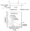
In some embodiments, the initiating event can be the UV laser absorption by the low melting glass (e.g., LMG or UVA) film. This can be based upon the larger absorbance of the thin film compared to Eagle XG® at 355 nm and the melting curves depicted in FIG. 3 . Considering the experimental arrangement illustrated in the top left portion of FIG. 3 , the laser was a Spectra Physics HIPPO 355 nm, generating 8-10 ns pulses at 30 kHz, up to 6.5 Watts of average power. The laser beam was focused to a 500 micron diameter beam waist, and the transmitted beam was monitored and sampled, yielding plots of the transmission percentage (% T) with time for different laser powers (5.0 W, 5.5 W, 6.0 W). These plots are shown in the lower left part of FIG. 3 . The onset of melting of the UVA, IRA or LMG film can be readily observed in FIG. 3 at lower laser power (bottom and middle curves) as the knee like inflection followed by rapid absorption and heating of the glass substrate, due to high local glass temperatures, which exceed Eagle XG®'s strain point. The glass parts being welded may not be melted but are rather only softened so they become pliant when held in intimate contact with a modest applied force. This behavior can be similar to solid state diffusion bonding, particularly in the ability to form strong bonds at between 50-80% of the substrate's melting temperature. An optical cross sectional image of the solid-state bond's birefringence illustrates a distinct interface line between the two parts being welded (see, e.g., FIG. 4 ).
Another embodiment includes welding with a 355-nm pulsed laser, producing a train of 1 ns pulses at 1 MHz, 2 MHz or 5 MHz repetition rates. When focusing the beam on the inorganic film into a spot between 0.02 mm and 0.15 mm diameter and welding with speeds ranging from 50 mm/s to 400 mm/s, defect-free bonding lines of approximately 60 μm to approximately 200 μm were produced. Required laser powers can range from approximately 1 W to approximately 10 W.
With reference to FIG. 4 , an experimental arrangement is illustrated which was used to estimate physical extent of laser welding bonding zone. With continued reference to FIG. 4 , two Eagle XG® slides were laser welded as previously described, mounted in a glass sandwich and cut with a diamond saw. This is illustrated in the left panel of FIG. 4 . The resulting cross section was mounted in a polarimeter to measure the optical birefringence resulting from local stress regions. This is shown in the right panel of FIG. 4 . The lighter regions in this right panel indicate more stress. As illustrated in the right panel of FIG. 4 , a bonded region appeared having a physical extent on the order 50 microns. Further, there does not appear to be any base or substrate glass melting, however, the bond formed between the two glass substrates was very strong. For example, the image in the center of the birefringence image cross section depicts a solid-state bond region extending deep (50 microns) into the Eagle XG® substrate which illustrates a high seal strength. Laser welding would include sweeping this zone along the interfacial boundaries to be bonded.
As noted in FIG. 3 , strong, hermetic, transparent bonds can be achieved using embodiments of the present disclosure by an exemplary low melting film or another film that absorbs/melts at an incident wavelength, color center formation in the film and glass, and temperature induced absorption in the film and glass. With regard to the first criterion, e.g., the low melting glass absorption event, laser illumination of the glass-LMG/UVA-glass structure with sufficiently high power per unit area can initiate absorption in the sputtered thin film LMG/UVA interface, inducing melting. This can be readily observed in the bottom curve of FIG. 3 in the lower left corner. The first downward slope of the bottom curve tracks the LMG/UVA melting process out to about 15 seconds, at which point another process occurs, this one being a glass-laser interaction (i.e., color center formation) in the respective substrate. The large curvature of this middle downward curve, after about 17 seconds would indicate a large absorption resulting from color centers forming in the glass. These color centers can generally be a function of the elemental impurity content in the substrate, e.g., As, Fe, Ga, K, Mn, Na, P, Sb, Ti, Zn, Sn to name a few. The more curvature in the transmission curve, the more color centers form. This is the second criterion noted in FIG. 3 . The melting point of the LMG/UVA film can be, but is not limited to, about 450° C., but the interfacial temperature can likely be above 660° C. based upon observations of a laser illumination experiment with a surrogate aluminum-coated EXG glass substrate under similar laser welding conditions. In this experiment, the aluminum melted (melting temperature: 660° C.), and the surface temperature was measured with a calibrated thermal imaging camera (FLIR camera) to be about 250° C. using laser welding conditions.
As noted above, color center formation plays a role in the formation of laser welds according to embodiments of the present disclosure. Modeling the basic color center formation processes under non-multiphoton conditions to derive a fitting function based on a three level diagram is illustrated in FIG. 7 using an experimental arrangement depicted in FIG. 8 . FIG. 7 is another modeling scheme according to embodiments of the present disclosure. In the left panel of FIG. 7 , three electronic glass band states absorb 355 nm photons, building up, or depleting population in the ground state ng[t], the conduction band ne[t], and color centers ncc[t]. It should be noted that single-headed arrows represent laser absorption, and double-headed arrows represent both stimulated absorption and emission. In the right panel of FIG. 7 , rate equations are provided which predict the smooth monotonic build up and depletion of electronic level populations while the coherently driven parts of the system exhibit rapid oscillations of the same populations (ng  ne). The initial conditions of the three levels are provided in the bottom row of the right panel of
 FIG. 7 . FIG. 8 is a diagram of an experimental arrangement for a 355 nm laser transmission (% T) through an Eagle 0.7 mm glass substrate for % T versus time measurements. With reference to FIG. 8 , diagnostic packaging can measure integrated energy and temporal waveform of UV pulses after passing through a fused silica window and Eagle XG® glass sheet with approximately 5 to 6 W being the average power.
Equation (1) below describes an experimental observable absorbance (Abs) versus time, e.g., related to transmission (trans) versus time data: (1≈Abs+Trans). The solution can be a sum of rising and decaying exponents, but can be simplified to following expression:
where α represents the linear absorption coefficient (cm−1), I represents the laser flux (photons/cm2·sec), σg represents the ground state absorption cross section (cm2), σesa, represents excited state absorption cross section (cm2), σcc represents the color-center absorption cross section (cm2), kec represents the transient color center rate, and kf represents the fluorescence decay rate. With reference to Equation (1) and
While the description heretofore has described laser welding of glass to glass substrates (of similar or different dimensions, geometries, and/or thicknesses), this should not limit the scope of the claims appended herewith as embodiments are equally applicable to substrates or sheets of non-glass materials, such as, but not limited to ceramics, glass-ceramics, metals, and the like with, or without, an interfacial conductive film. For example, FIG. 12 is an illustration of an experiment assessing the extent of laser welding over ITO leads. With reference to FIG. 12 , an LMG-coated Eagle XG® slide is illustrated laser welded to an ITO-coated Eagle XG® slide in the left panel of the figure. In this experiment, a 100 nm ITO film was deposited onto Eagle XG® substrates by reactive sputtering through a mask. Conditions were selected resulting in ITO films having a relatively high average sheet resistance of approximately 126Ω per square (Ω/sq), with a standard-deviation of 23 Ω/sq, reflecting that no thermal heating of the substrate was employed, before, during or after, the reactive sputtering deposition. The ITO film appears in FIG. 12 as a distinct yellowish or shaded strip, diagonally distributed in the photograph. Multimeter measurements of 350Ω were recorded over the distance indicated, prior to laser welding. An LMG-coated Eagle XG® slide was then laser welded to an ITO-coated Eagle XG® slide whereby it was discovered that the laser weld line was quite distinct, strong, transparent, and diagonally distributed but inverted. In the right panel of FIG. 12 , post laser-weld measurement of the resistance across the ITO leads over the same distance used earlier was observed to increase the resistance from 350Ω to 1200Ω. The drop in conductivity was due to partial damage of the ITO film as the ITO film absorbed 355 nm radiation. To avoid damage of ITO film due to overheating, however, embodiments can change laser parameters so temperature at the interface does not transition from bare glass substrate to ITO film substrate or otherwise (e.g., variable peak power, variable repetition rate, variable average power, variable translation speed of the beam, electrode pattern, LMG film thickness, etc.).
Applications that may utilize embodiments described herein having efficient formation of high bond-strength, transparent, glass-to-glass welds are numerous and include, but are not limited to, solid state lighting, display, and transparent vacuum insulated technologies. Laser welding of glass, in particular, can provide efficiencies and features such as a small heat affected zone (HAZ) that many traditional welding methods, such as e-beam, arc, plasma, or torch simply cannot provide. In some embodiments, laser glass welding can generally proceed without pre- or post-heating using infrared (IR) lasers for which many glasses are opaque or ultra-short pulse lasers (USPL) for which many glasses are transparent. In some embodiments, a judicious choice of glass substrate compositions and interfacially distributed IR absorbing frit can make hermetic glass “sandwich-type” laser sealed packages possible. In some embodiments, ultra-short pulsed lasers can be focused at either surface or interior points in an exemplary glass substrate and can induce absorption by non-linear processes such as multi-photon or avalanche ionization.
Heretofore, a low-power laser-welding process has been described that relies on an absorbing low melting glass interfacial film and can be attributed to diffusion welding, owing to its low temperature bond formation (as low as half the melting temperature), and requirement for contact and pressure conditions. As discussed above, several effects were notable to laser welding glass sheets together with strong bond formation, e.g., an absorbing low melting glass film at the incident laser wavelength, laser induced color centers formed in the glass substrates, and thermal induced absorption in the substrate to effectively accelerating the temperature increase.
In some embodiments, however, many films highly absorbing at an incident wavelength (e.g., 355 nm) can be sufficient to induce high bond strength laser welds. Other films, for example, ZnO or SnO2, are chemically different than some exemplary low melting glass compositions described herein but share the same laser welding capability at a relatively low light flux. Thus, it was discovered that the low melting character may not be necessary in some embodiments, in light of the melting temperature of ZnO (1975° C.) as compared with some low melting glass compositions (˜450° C.). It was discovered, however, that a unifying characteristic of these films was that they absorb radiation substantially at 355 nm: ZnO absorbance˜45% (200 nm thick film), and low melting glass ˜15% (200 nm thick film). It was also determined that exemplary methods described herein could laser weld quartz, or pure fused silica substrates—i.e., substrates without color centers. Thus, it has been determined that color centers are not necessarily essential but may be needed in some embodiments when absorption of an exemplary film is low (e.g., ˜Abs<20%).
As noted above with reference to FIG. 3 , it was discovered that optimum welding can be a function of three mechanisms, namely, absorption by an exemplary film and/or substrate of laser radiation and the heating effect based of this absorption process, increase of the film and substrate absorption due to the heating effects (band gap shift to the longer wavelength) which can be transient and depends upon the processing conditions, and defect or impurity absorption or color center absorption generated by UV radiation. Thermal distribution can be an important aspect of this process, and the discussion below can be used to assist in the understanding of temperature distribution at the interface between two substrates, assuming static absorption at the interface.
El-Adawi developed an analytical model of laser-heating a two-layer stack consisting of an absorbing film of thickness Z, on a large semi-infinite slab substrate. The heat diffusion equation in each material was solved with matched boundary conditions yielding expressions of temperature as a function of time and position with the film and substrate: Tf(t, z), Ts(t, z). El-Adawi's model assumed thermal properties (diffusivity, D, conductivity, k, heat capacity, Cp) of the film and substrate were fixed, such that absorption occurred only in the surface and no phase changes occurred. Laplace transforms were used yielding summations with exponential and error (complementary) function terms:
where Af represents the surface absorbance of the thin film, Io represents the laser flux (photons/cm2·sec), n represents an integer (0≦n≦∞), and all subscripts, f, refer to the film parameters while subscripts, s, refer to the substrate's parameters. B, and ε are related to material properties: B=1−ε/1+ε<1, ε=(ks/kf)√Df/Ds), while Lf also includes time t: Lf 2=4Dft. The time and space range for the thin film layer can be provided as: 0<t, 0≦zf≦Z, respectively, where Z represents the film thickness. The time and space range for the substrate layer are provided as: ts<t, Z≦zs≦∞, respectively, where ts represents the time it takes the temperature of the film's backside to begin deviation from room temperature after initial laser-film incidence (ts=Z2/6Df). Expansion coefficients are related to independent variables and material properties through the following expression:
Temperature variations due to using different laser powers, or films with differing absorbance were also explored as illustrated in FIG. 17 . FIG. 17 is a series of temperature variation plots for some embodiments. With reference to FIG. 17 , glass substrate temperature distribution dependence on laser power and film absorbance was plotted using the two-layer laser-heating model (Equation (2)). The same laser parameters used in FIG. 16 were used in FIG. 17 . More specifically, a pulsed UV laser with the following parameters was used: λ=355 nm, beam waist=500 μm, repetition rate=30,000 Hz, and pulse width=10 ns. As can be observed in the left panel of FIG. 17 , the influence of laser power on the substrate temperature distribution appears more linear as compared with the higher order behavior of absorbance in the right panel of FIG. 17 . This behavior is not obvious from Equation (2) where power, Io, and absorbance, Af, appear coupled. Absorbance can indirectly impact the effective film thickness, Zf, for which the expansion coefficients bn and gn are somewhat related. In contrast, Io is independent, with no functional relationship associated with the expansion coefficients bn, and gn.
Exploring a potential mechanism underlying laser welding dynamics, diffusion-weld creep flow, it can be observed that relatively low temperature bond formation occurs as low as half the melting temperature of the glass substrates, and that contact and pressure conditions may be required in some embodiments. Mass transport of mostly substrate material into the gap occurs in a manner consistent with hot swelling expanding glass activated by temperatures above the substrate strain point. The movement of this material can be described by one of various forms of creep flow typically found in diffusion welding models, namely, viscous, plastic, or diffusive transport processes. While these models are often used in the description of metal welding, they can be adapted for the present case, using the notion of relative contact area, Ac/A0, and its kinetic development illustrated in FIG. 26 . FIG. 26 is a schematic illustration of the evolution of relative contact area, Ac/A0, during laser welding of the interfacial gap region under constant applied pressure Pext. With reference to FIG. 26 , in the top panel, time=0 and the initial condition of the relative contact area Ac/A0=0. In the middle panel, time is greater than 0 illustrating an intermediate state of the interfacial gap region where Ac/A0>0. In the bottom pane, time is at a predetermined point (t≈end) where the weld or bond is essentially complete and the gap is effectively non-existent, Ac/A0, ≈1. Formation of a diffusion-welded interface typified by FIG. 26 assumes an evolution of relative contact area, Ac/A0, that converges to distances at which chemical bonds form. An approximation can be employed to describe these kinetics:
where k represents a constant, p represents pressure, n represents a pressure exponent, and Q represents an activation energy of the specific rate-controlling creep-flow mechanism. The value of n can be correlated with the rate-controlling mechanism as follows: n=1, for viscous mass transport; n=2, for plastic flow; n=3, for evaporative/condensation transport; and n>3, for diffusive transport.
Equation (4) can be employed as a guide in deducing some mechanistic forces at work since the expression assumes isothermal conditions. To begin this mechanistic exploration and because of its similarity to Eagle XG® (softening point: 971° C.), parameters can be used from the literature of a 3-point bend experimental study over the range from 800° C.-950° C., of the high temperature creep of low softening-point boro-silicate glass (700° C.-750° C.) where it was found, for all stages of creep, that deformation behavior exhibited linear viscoelasticity controlled by viscous flow for both fast and slow creep regimes. Using fast creep regime data (n=1, Q=160 kJ/mol, and k=0.00048 Pa−1s), with conditions similar to some laser welding experiments (950° C.), the total effective pressure of the weld area can be estimated, Ptotal, at 950° C. as 600 MPa assuming Eagle XG®'s nominal modulus and CTE values of 73.6 GPa and 3.1 ppm/° C. apply, beyond that of the nominal applied pressure of about 0.1 MPa. This upper bound estimation was based on experimental data measured indicating substrate glass, and film material, swelling and expanding above the planar interface region as illustrated in FIG. 27 . FIG. 27 illustrates a profilometer trace over a laser sweep region of an embodiment using typical laser welding conditions. With reference to FIG. 27 , the bottom schematic represents a single low melting glass coated (1 μm thick film) Eagle XG® substrate subjected to two successive laser sweeps under the following conditions: 355 nm, 30 kHz, 4 mm/sec translation rate. The top image of FIG. 27 is a single-line profilometer trace over these two weld regions indicating a raised morphology.
Even assuming temperature is fixed at 950° C., it may be noted whether the viscous flow mechanism under that condition is sufficient in forming and driving diffusion welds to completion (Ac/A0≈1). FIG. 28 provides some insight to this case. FIG. 28 is a series of plots providing a comparison of welding rate estimates for some embodiments. With reference to FIG. 28 , a comparison of welding rate estimates can be based upon Equation (4) using low strain and softening point boro-silicate glass creep flow parameters and an effective welding pressure of 600 MPa. The two plots differ only in assuming either viscous flow prevails (left plot) or plastic flow (right plot). Recalling that dwell times on the order of 0.25 seconds yield strong laser welds under about 6 Watts and 30 kHz laser repetition rate conditions, the viscous flow interpretation may be questioned, and the left plot in FIG. 28 suggests other mechanisms, e.g., plastic flow, that may also account for the strong weld formation.
where terms are identical with those used in Equation (2), except that Z represents the melt front location, QL represents the latent heat of melting, and that heat flow is one dimensional, optical radiation is absorbed at the surface, and thermal material properties remain temperature independent. Quadratic equations can then be derived in both Z and dZ/dt having coefficients that are functions of thermo-physical and laser parameters. To understand dependences of a propagating stress field, the propagating laser melt front analytic model may be modified by substituting the latent heat of melting (fusion) of Eagle XG® with the activation energy for creep flow from our previous Eagle XG® surrogate: the low strain point boro-silicate glass normalized with its effective molecular weight (160 kJ/mol)/(0.266 kg/mol). Considering the case where no heat is dissipated from the back of the slab substrate during the weld, the resulting expression exhibits interesting dependencies on laser and material properties:
where Z represents creep front location, l represents substrate thickness, Cp represents substrate heat capacity, A represents substrate absorbance, R represents substrate reflectance, ΔTm represents propagating temperature increase, from ambient, required for maintaining creep flow (e.g., ΔTm=Tstrain−Tambient), ρ represents substrate density, λ represents substrate thermal conductivity, I0 represents laser irradiance (W/m2), and t represents time.
Power dependence is illustrated in FIG. 30 whereby it can be observed that simply increasing laser power during welding can induce greater stress beyond the interface region with excess energy resulting in a larger stress. FIG. 30 is a plot providing stress location from an exemplary weld line. With reference to FIG. 30 , stress location from an exemplary weld line can be determined using Equation (6) where the parameters employed were similar to those used previously: wavelength=355 nm, beam waist=500 μm, repetition rate=30,000 Hz, pulse width=10 ns, vs=2 mm/sec, dwell time=0.25 second, Eagle XG® thickness=0.7 mm, and Tstrain=669° C. FIG. 30 and Equation (6) also provide insight into why higher strain point glass substrates can result in higher stress profiles. For example, the stress profile location Z scales as the square root of the ΔTm term which is linearly related to Tstrain. Other attempts to predict experimental observations from these expressions can be limited not only by the assumptions used but also by the information that can be calculated, e.g., where higher CTE materials are laser welded. Here it was discovered that low CTE glass substrates (less than about 5 ppm/° C.) were more easily welded than higher CTE glasses such as soda-lime glasses. These low CTE substrates included quartz, fused silica, Eagle XG®, Willow, and Lotus glass substrates. After significant experimentation, suitable conditions were discovered making high quality welds in higher CTE glasses possible. For example, it was discovered that embodiments described herein can be used to weld soda lime glass (CTEs of about 9 ppm/° C. or greater) using 1 μm LMG films without any pre-heating requirement of the substrates, much less to the strain or annealing point. FIG. 31 is a series of photographs of laser welded soda lime glass according to some embodiments. With reference to FIG. 31 , a high quality bond formation was achieved using very low laser power and a nanosecond pulse-width UV (355 nm) laser. The laser weld conditions used for these non-limiting and illustrated welds included a pulse width=1 ns, repetition rate=5 MHz, power=1 Watt, an approximately 20 μm beam spot resulting in 67 μm weld line, and vs=50 mm/s. With continued reference to FIG. 31 , a pulsed, 355-nm laser was used to weld two 0.7 mm thick soda lime glass plates compressed together with one substrate having a sputtered 1 μm thick low melting glass film. The aforementioned example and experiment should not limit the scope of the claims appended herewith as ranges of 2 MHz and 5 MHz laser repetition rates with 1 ns pulse widths were explored at laser beam translation rates from 50 mm/s-400 mm/sec. Further, laser beam spots of approximately 20 μm-70 μm at the low melting glass film interface were also explored for exemplary welds. In some embodiments, an exemplary weld line quality can be observed with a focal spot size of about 20 μm and a 50 mm/s translation rate. The robustness of these welded substrates was also noted after subjecting them to 100° C. for 4 hours without any crack formation.
In some embodiments, laser welds can be achieved using a film that absorbs at an incident laser wavelength λ, preferably A %> about 20%. In other embodiments, both the substrate and film can exhibit color center formation at λ. In additional embodiments, a temperature effect can be employed to increase absorption for either or both the film and substrate at λ. Such an exemplary temperature effect can also contribute to the improvement of seal or weld speed and can lower the heat affected zone (HAZ) and can lower activation energy for creep flow, e.g., forms an eutectic system, an alloy, etc. In some embodiments, if transparency is required, then a band gap may be provided in UV, or high absorption in NIR, IR. Additional embodiments can provide a weld having an interfacial surface energy γweld-interface>>residual γstress field and/or a total integrated bond strength ∫∫γweld-interface ∂A>>∫∫γstress-field∂A. Further embodiments can include a low laser intensity requirement whereby the laser peak photon flux is less than about 1025 photons/sec/cm2 and does not include multiphoton behavior, ablation, or plasma generation.
While some embodiments have been described as utilizing low melting glass or inorganic films, the claims appended herewith should not be so limited as embodiments can use UV absorbing films, IRA films, and/or other inorganic films situated between two substrates. As noted above, in some embodiments, color center formation in an exemplary substrate glass is not necessary and is a function of the UV absorption of the film, e.g., less than about 20%. It follows that, in other embodiments, if the UV absorption of the film is greater than about 20%, alternative substrates such as quartz, low CTE substrates, and the like, can readily form welds. Furthermore, when high CTE substrates are used, these substrates can be readily welded with exemplary high repetition rate lasers (e.g., greater than about 300 kHz to about 5 MHz) and/or a low peak power. Furthermore, in embodiments where absorption of the film is a contributing factor, IR absorbing (visible transparent films) can be welded with the use of an exemplary IR laser system.
In various embodiments of the present disclosure, the glass sealing materials and resulting layers can be transparent and/or translucent, thin, impermeable, “green,” and configured to form hermetic seals at low temperatures and with sufficient seal strength to accommodate large differences in CTE between the sealing material and the adjacent substrates. In some embodiments, the sealing layers can be free of fillers and/or binders. The inorganic materials used to form the sealing layer(s) can be non-frit-based or powders formed from ground glasses in some embodiments (e.g., UVA, LMG, etc.). In other embodiments, the sealing layer material is a low Tg glass that has a substantial optical absorption cross-section at a predetermined wavelength which matches or substantially matches the operating wavelength of a laser used in the sealing process. In additional embodiments, absorption at room temperature of a laser processing wavelength by the low Tg glass layer is at least 15%.
In general, suitable sealant materials include low Tg glasses and suitably reactive oxides of copper or tin. The glass sealing material can be formed from low Tg materials such as phosphate glasses, borate glasses, tellurite glasses and chalcogenide glasses. As defined herein, a low Tg glass material has a glass transition temperature of less than 400° C., e.g., less than 350, 300, 250 or 200° C. Exemplary borate and phosphate glasses include tin phosphates, tin fluorophosphates and tin fluoroborates. Sputtering targets can include such glass materials or, alternatively, precursors thereof. Exemplary copper and tin oxides are CuO and SnO, which can be formed from sputtering targets comprising pressed powders of these materials. Optionally, the glass sealing compositions can include one or more dopants, including but not limited to tungsten, cerium and niobium. Such dopants, if included, can affect, for example, the optical properties of the glass layer, and can be used to control the absorption by the glass layer of laser radiation. For instance, doping with ceria can increase the absorption by a low Tg glass barrier at laser processing wavelengths. Additional suitable sealant materials include laser absorbing low liquidus temperature (LLT) materials with a liquidus temperature less than or equal to about 1000° C., less than or equal to about 600° C., or less than or equal to about 400° C. In other embodiments, the composition of the inorganic film can be selected to lower the activation energy for inducing creep flow of the first substrate, the second substrate, or both the first and second substrates as described above.
Exemplary tin fluorophosphate glass compositions can be expressed in terms of the respective compositions of SnO, SnF2 and P2O5 in a corresponding ternary phase diagram. Suitable UVA glass films can include SnO2, ZnO, TiO2, ITO, and other low melting glass compositions. Suitable tin fluorophosphates glasses include 20-100 mol % SnO, 0-50 mol % SnF2 and 0-30 mol % P2O5. These tin fluorophosphates glass compositions can optionally include 0-10 mol % WO3, 0-10 mol % CeO2 and/or 0-5 mol % Nb2O5. For example, a composition of a doped tin fluorophosphate starting material suitable for forming a glass sealing layer comprises 35 to 50 mole percent SnO, 30 to 40 mole percent SnF2, 15 to 25 mole percent P2O5, and 1.5 to 3 mole percent of a dopant oxide such as WO3, CeO2 and/or Nb2O5. A tin fluorophosphate glass composition according to one particular embodiment can be a niobium-doped tin oxide/tin fluorophosphate/phosphorus pentoxide glass comprising about 38.7 mol % SnO, 39.6 mol % SnF2, 19.9 mol % P2O5 and 1.8 mol % Nb2O5. Sputtering targets that can be used to form such a glass layer may include, expressed in terms of atomic mole percent, 23.04% Sn, 15.36% F, 12.16% P, 48.38% 0 and 1.06% Nb.
A tin phosphate glass composition according to another embodiment comprises about 27% Sn, 13% P and 60% O, which can be derived from a sputtering target comprising, in atomic mole percent, about 27% Sn, 13% P and 60% O. As will be appreciated, the various glass compositions disclosed herein may refer to the composition of the deposited layer or to the composition of the source sputtering target. As with the tin fluorophosphates glass compositions, example tin fluoroborate glass compositions can be expressed in terms of the respective ternary phase diagram compositions of SnO, SnF2 and B2O3. Suitable tin fluoroborate glass compositions include 20-100 mol % SnO, 0-50 mol % SnF2 and 0-30 mol % B2O3. These tin fluoroborate glass compositions can optionally include 0-10 mol % WO3, 0-10 mol % CeO2 and/or 0-5 mol % Nb2O5. Additional aspects of suitable low Tg glass compositions and methods used to form glass sealing layers from these materials are disclosed in commonly-assigned U.S. Pat. No. 5,089,446 and U.S. patent application Ser. Nos. 11/207,691, 11/544,262, 11/820,855, 12/072,784, 12/362,063, 12/763,541, 12/879,578, and 13/841,391 the entire contents of which are incorporated by reference herein.
Exemplary substrates (glass or otherwise) can have any suitable dimensions. Substrates can have areal (length and width) dimensions that independently range from 1 cm to 5 m (e.g., 0.1, 1, 2, 3, 4 or 5 m) and a thickness dimension that can range from about 0.5 mm to 2 mm (e.g., 0.5, 0.6, 0.7, 0.8, 0.9, 1.0, 1.2, 1.5 or 2 mm). In further embodiments, a substrate thickness can range from about 0.05 mm to 0.5 mm (e.g., 0.05, 0.1, 0.2, 0.3, 0.4 or 0.5 mm). In still further embodiments, a glass substrate thickness can range from about 2 mm to 10 mm (e.g., 2, 3, 4, 5, 6, 7, 8, 9 or 10 mm). A total thickness of an exemplary glass sealing layer can range from about 100 nm to 10 microns. In various embodiments, a thickness of the layer can be less than 10 microns, e.g., less than 10, 5, 2, 1, 0.5 or 0.2 microns. Exemplary glass sealing layer thicknesses include 0.1, 0.2, 0.5, 1, 2, 5 or 10 microns. The width of the sealed region, which can be proportional to the laser spot size, can be about 0.05 to 2 mm, e.g., 0.05, 0.1, 0.2, 0.5, 1, 1.5 or 2 mm. A translation rate of the laser (i.e., sealing rate) can range from about 1 mm/sec to 1000 mm/sec, such as 1, 2, 5, 10, 20, 50, 100, 200, 400, or 1000 mm/sec. The laser spot size (diameter) can be about 0.02 to 1 mm.
Thus, it has been discovered that suitable laser welding glass substrate interfaces can occur in embodiments of the present disclosure when the local glass temperature exceeds its strain or annealing temperature (e.g., 669° C. and 772° C. respectively for EXG) within a spatial extent, e.g., the “welding volume”. This volume can be dependent upon the incident laser power, the composition of the UVA or LMG melt, and color center formation (as a result of impurities in the respective substrates). Once attained, the volume can be swept over the interfacial regions to result in a rapid and strong seal between two substrates (glass or otherwise). Sealing speeds in excess of 5-1000 mm/s can be attained. Exemplary laser welds can experience an abrupt transition to relatively cold ambient temperatures from the high temperatures associated with the melt volume as it is swept away over the substrate regions of interest. The integrity of the hermetic seal and its respective strength can be maintained by slow cooling (self-annealing) of the hot base glass color center (relaxation) regions and the thinness of the UVA or LMG or NIR thin film region (typically ½-1 μm) thereby nullifying any impact of CTE mismatching between the two respective substrates (glass or otherwise).
According to embodiments, the choice of the sealing layer material and the processing conditions for forming a sealing layer over a glass substrate are sufficiently flexible that the substrate is not adversely affected by formation of the glass layer. Low melting temperature glasses can be used to seal or bond different types of substrates. Sealable and/or bondable substrates include glasses, glass-glass laminates, glass-polymer laminates, glass-ceramics or ceramics, including gallium nitride, quartz, silica, calcium fluoride, magnesium fluoride or sapphire substrates. Additional substrates can be, but are not limited to, metal substrates including tungsten, molybdenum, copper, or other types of suitable metal substrates. In some embodiments, one substrate can be a phosphor-containing glass plate, which can be used, for example, in the assembly of a light emitting device. A phosphor-containing glass plate, for example, comprising one or more of a metal sulfide, metal silicate, metal aluminate or other suitable phosphor, can be used as a wavelength-conversion plate in white LED lamps. White LED lamps typically include a blue LED chip that is formed using a group III nitride-based compound semiconductor for emitting blue light. White LED lamps can be used in lighting systems, or as backlights for liquid crystal displays, for example. The low melting temperature glasses and associate sealing method disclosed herein can be used to seal or encapsulate the LED chip.
Exemplary processes according to embodiments of the present disclosure can be made possible because of the base substrate (glass or otherwise) properties due to the ability of the substrate to form color centers with the prevailing laser illumination conditions and resulting temperature enhancement. In some embodiments, the color center formation can be reversible if transparent seals are desired. If the substrates have dissimilar thicknesses, then thermally conductive substrates can be employed in some embodiments to restore weld integrity.
Exemplary embodiments can thus utilize low melting temperature materials to laser-weld glass or other material substrates together with a low laser pulse peak-power to minimize creation of shock waves and to ensure no micro cracks appear which could compromise the tensile fracture strength. Exemplary embodiments can also provide diffusion welding without melt puddle propagation allowing an adequate lower temperature sealing process. Due to the thinness of the film region, embodiments of the present disclosure can nullify any impact of CTE mismatching between the two respective substrates and can be utilized to provide welding of similarly or dissimilarly dimensioned substrates. Further, in embodiments of the present disclosure no patterning of film is required for sealing as occurs in the case of frit or staining materials, and manufacturers therefore do not have to reveal their proprietary designs.
The present disclosure also teaches how low melting temperature materials can be used to laser weld glass packages together enabling long lived hermetic operation of passive and active devices sensitive to degradation by attack of oxygen and moisture. As noted above, embodiments described herein provide UVA, LMG or other seals that can be thermally activated after assembly of the bonding surfaces using laser absorption and can enjoy a higher manufacturing efficiency since the rate of sealing each working device can be determined by thermal activation and bond formation, rather than the rate one encapsulates a device by inline thin film deposition in a vacuum or inert gas assembly line. This can enable large sheet multiple device sealing with subsequent scoring into individual devices (singulation), and due to high mechanical integrity the yield from singulation can be high.
Embodiments of the present disclosure also provide a laser sealing process, e.g., laser welding, diffusing welding, etc., that relies upon color center formation within the glass substrates due to extrinsic color centers, e.g., impurities or dopants, or intrinsic color centers inherent to the glass, at an incident laser wavelength, combined with exemplary laser absorbing films. Some non-limiting examples of films include SnO2, ZnO, TiO2, ITO, and low melting glass films which can be employed at the interface of the glass substrates. Welds using these materials can provide visible transmission with sufficient UV absorption to initiate steady state gentle diffusion welding. These materials can also provide transparent laser welds having localized sealing temperatures suitable for diffusion welding. Such diffusion welding results in low power and temperature laser welding of the respective glass substrates and can produce superior transparent welds with efficient and fast welding speeds. Exemplary laser welding processes according to embodiments of the present disclosure can also rely upon photo-induced absorption properties of glass beyond color center formation to include temperature induced absorption.
Hermetic encapsulation of a workpiece using the disclosed materials and methods can facilitate long-lived operation of devices otherwise sensitive to degradation by oxygen and/or moisture attack. Example workpieces, devices or applications include flexible, rigid or semi-rigid organic LEDs, OLED lighting, OLED televisions, photovoltaics, MEMs displays, electrochromic windows, fluorophores, alkali metal electrodes, transparent conducting oxides, quantum dots, etc.
As used herein, a hermetic layer is a layer which, for practical purposes, is considered substantially airtight and substantially impervious to moisture and/or oxygen. By way of example, the hermetic seal can be configured to limit the transpiration (diffusion) of oxygen to less than about 10−2 cm3/m2/day (e.g., less than about 10−3 cm3/m2/day), and limit the transpiration (diffusion) of water to about 10−2 g/m2/day (e.g., less than about 10−3, 10−4, 10−5 or 10−6 g/m2/day). In embodiments, the hermetic seal substantially inhibits air and water from contacting a protected workpiece.
In some embodiments, a method of bonding two substrates comprises forming a first glass layer on a sealing surface of a first substrate, forming a second glass layer on a sealing surface of a second substrate, placing at least a portion of the first glass layer in physical contact with at least a portion of the second glass layer, and heating the glass layers to locally melt the glass layers and the sealing surfaces to form a glass-to-glass weld between the first and second substrates. In each of the sealing architectures disclosed herein, sealing using a low melting temperature glass layer can be accomplished by the local heating, melting and then cooling of both the glass layer and the glass substrate material located proximate to the sealing interface.
It is thus an aspect of embodiments of the present disclosure to combine the ease of forming hermetic seals associated with laser welding to also form hermetic packages of active OLED or other devices to enable their widespread fabrication. Such fabrication would require welding over interfacial conductive films. Unlike the methods disclosed herein, conventional methods of laser sealing can sever such interfacial conducting leads would sever them especially if the interface temperature gets too high or there is deleterious laser radiation interaction with the conducting lead material. Embodiments of the present disclosure, however, provide an enabling disclosure of device structures requiring electrical biasing for hermetic device operation using interfacial low melting temperature glass material film. Embodiments of the present subject matter may thus provide a successful laser-welding of glass sheets or other substrates having an interfacial conductive film without destruction thereto or loss in performance.
In some embodiments, a method of bonding a workpiece comprises forming an inorganic film over a surface of a first substrate, arranging a workpiece to be protected between the first substrate and a second substrate wherein the film is in contact with the second substrate, and bonding the workpiece between the first and second substrates by locally heating the film with laser radiation having a predetermined wavelength. The inorganic film, the first substrate, or the second substrate can be transmissive at approximately 420 nm to approximately 750 nm. In another embodiment, each of the inorganic film, first substrate and second substrate are transmissive at approximately 420 nm to approximately 750 nm. In a further embodiment, absorption of the inorganic film is more than 10% at a predetermined laser wavelength. In an additional embodiment, the composition of the inorganic film can be, but is not limited to, SnO2, ZnO, TiO2, ITO, Zn, Ti, Ce, Pb, Fe, Va, Cr, Mn, Mg, Ge, SnF2, ZnF2 and combinations thereof. In other embodiments, the composition of the inorganic film can be selected to lower the activation energy for inducing creep flow of the first substrate, the second substrate, or both the first and second substrates. In another embodiment, the composition of the inorganic film can be a laser absorbing low liquidus temperature material with a liquidus temperature less than or equal to about 1000° C., less than or equal to about 600° C., or less than or equal to about 400° C. In further embodiments, the step of bonding can create a bond having an integrated bond strength greater than an integrated bond strength of a residual stress field in the first substrate, second substrate or both the first and second substrates. In some exemplary embodiments, such a bond will fail only by cohesive failure. In a further embodiment, the composition of the inorganic film comprises 20-100 mol % SnO, 0-50 mol % SnF2, and 0-30 mol % P2O5 or B2O3. In some embodiments, the inorganic film and the first and second substrates have a combined internal transmission of more than 80% at approximately 420 nm to approximately 750 nm. In other embodiments, the step of bonding further comprises bonding the workpiece between the first and second substrates as a function of the composition of impurities in the first or second substrates and as a function of the composition of the inorganic film though the local heating of the inorganic film with laser radiation having a predetermined wavelength. Exemplary impurities in the first or second substrates can be, but are not limited to, As, Fe, Ga, K, Mn, Na, P, Sb, Ti, Zn, Sn and combinations thereof. In further embodiments, the first and second substrates have different lateral dimensions, different CTEs, different thicknesses, or combinations thereof. In some embodiments, one of the first and second substrates can be glass or glass-ceramic. Of course, the other of the first and second substrates can be a glass-ceramic, ceramic or metal. In some embodiments, the method can also include the step of annealing the bonded workpiece. In other embodiments, the laser radiation comprises UV radiation at a predetermined wavelength between approximately 193 nm to approximately 420 nm, NIR radiation at a predetermined wavelength between approximately 780 nm to approximately 5000 nm, can include a pulse-width from 1 to 40 nanoseconds and a repetition rate of at least 1 kHz, and/or can be continuous wave. In further embodiments, a thickness of the inorganic film ranges from about 10 nm to 100 micrometers. In some embodiments, the first, second or first and second substrates can comprise an alkaline earth boro-aluminosilicate glass, thermally strengthened glass, chemically strengthened glass, boro-silicate glass, alkali-aluminosilicate glass, soda-lime glass, and combinations thereof. In other embodiments, the method can include the step of moving a laser spot formed by the laser radiation at a speed of approximately 1 mm/s to approximately 1000 mm/s to create a minimal heating zone. This speed, in some embodiments, does not exceed the product of a diameter of the laser spot and a repetition rate of the laser radiation. In further embodiments, the step of bonding can create a bond line having a width of approximately 50 μm to approximately 1000 μm. In other embodiments, the inorganic film, first substrate, or second substrate can be optically transparent before and after the step of bonding in a range of greater than 80%, between 80% to 90%, greater than 85%, or greater than 90% at about 420 nm to about 750 nm. An exemplary workpiece can be, but is not limited to, a light emitting diode, an organic light emitting diode, a conductive lead, a semiconductor chip, an ITO lead, a patterned electrode, a continuous electrode, quantum dot materials, phosphor, and combinations thereof.
In other embodiments, a bonded device is provided comprising an inorganic film formed over a surface of a first substrate, and a device protected between the first substrate and a second substrate wherein the inorganic film is in contact with the second substrate. In such an embodiment, the device includes a bond formed between the first and second substrates as a function of the composition of impurities in the first or second substrates and as a function of the composition of the inorganic film though a local heating of the inorganic film with laser radiation having a predetermined wavelength. Further, the inorganic film, the first substrate, or the second substrate can be transmissive at approximately 420 nm to approximately 750 nm. In another embodiment, each of the inorganic film, first substrate and second substrate are transmissive at approximately 420 nm to approximately 750 nm. In a further embodiment, absorption of the inorganic film is more than 10% at a predetermined laser wavelength. In an additional embodiment, the composition of the inorganic film can be, but is not limited to, SnO2, ZnO, TiO2, ITO, Zn, Ti, Ce, Pb, Fe, Va, Cr, Mn, Mg, Ge, SnF2, ZnF2 and combinations thereof. In other embodiments, the composition of the inorganic film can be selected to lower the activation energy for inducing creep flow of the first substrate, the second substrate, or both the first and second substrates. In another embodiment, the composition of the inorganic film can be a laser absorbing low liquidus temperature material with a liquidus temperature less than or equal to about 1000° C., less than or equal to about 600° C., or less than or equal to about 400° C. In further embodiments, the bond can have an integrated bond strength greater than an integrated bond strength of a residual stress field in the first substrate, second substrate or both the first and second substrates. In some exemplary embodiments, such a bond will fail only by cohesive failure. In a further embodiment, the composition of the inorganic film comprises 20-100 mol % SnO, 0-50 mol % SnF2, and 0-30 mol % P2O5 or B2O3. In some embodiments, the inorganic film and the first and second substrates have a combined internal transmission of more than 80% at approximately 420 nm to approximately 750 nm. Exemplary impurities in the first or second substrates can be, but are not limited to, As, Fe, Ga, K, Mn, Na, P, Sb, Ti, Zn, Sn and combinations thereof. In further embodiments, the first and second substrates have different lateral dimensions, different CTEs, different thicknesses, or combinations thereof. In some embodiments, one of the first and second substrates can be glass or glass-ceramic. Of course, the other of the first and second substrates can be a glass-ceramic, ceramic or metal. In further embodiments, a thickness of the inorganic film ranges from about 10 nm to 100 micrometers. In some embodiments, the first, second or first and second substrates can comprise an alkaline earth boro-aluminosilicate glass, alkali-aluminosilicate glass, thermally strengthened glass, chemically strengthened glass, soda-lime glass, boro-silicate glass and combinations thereof. In other embodiments, the inorganic film, first substrate, or second substrate can be optically transparent before and after the step of bonding in a range of greater than 80%, between 80% to 90%, greater than 85%, or greater than 90% at about 420 nm to about 750 nm. An exemplary device can be, but is not limited to, a light emitting diode, an organic light emitting diode, a conductive lead, a semiconductor chip, an ITO lead, a patterned electrode, a continuous electrode, quantum dot materials, phosphor, and combinations thereof. In some embodiments, the bond can be hermetic with a closed loop or with seal lines crossing at angles greater than about 1 degree, can include spatially separated bond spots, and/or can be located at less than about 1000 μm from heat sensitive material of the bond. In other embodiments, birefringence around the bond can be patterned.
In further embodiments, a method of protecting a device is provided comprising forming an inorganic film layer over a first portion surface of a first substrate, arranging a device to be protected between the first substrate and a second substrate wherein the sealing layer is in contact with the second substrate, and locally heating the inorganic film layer and the first and second substrates with laser radiation to melt the sealing layer and the substrates to form a seal between the substrates. The first substrate can be comprised of glass or glass-ceramics, and the second substrate can be comprised of metal, glass-ceramics or ceramic. In some embodiments, the first and second substrates have different lateral dimensions, different CTEs, different thicknesses, or combinations thereof. In other embodiments, the device can be, but is not limited to, an ITO lead, a patterned electrode, and a continuous electrode. In some embodiments, the step of locally heating further comprises adjusting power of the laser radiation to reduce damage to the formed seal. An exemplary film can be, but is not limited to, a low Tg glass, which comprises 20-100 mol % SnO, 0-50 mol % SnF2, and 0-30 mol % P2O5 or B2O3. In other embodiments, the composition of the inorganic film can be selected to lower the activation energy for inducing creep flow of the first substrate, the second substrate, or both the first and second substrates. In another embodiment, the composition of the inorganic film can be a laser absorbing low liquidus temperature material with a liquidus temperature less than or equal to about 1000° C., less than or equal to about 600° C., or less than or equal to about 400° C. In further embodiments, the step of bonding can create a bond having an integrated bond strength greater than an integrated bond strength of a residual stress field in the first substrate, second substrate or both the first and second substrates. In some exemplary embodiments, such a bond will fail only by cohesive failure.
While this description can include many specifics, these should not be construed as limitations on the scope thereof, but rather as descriptions of features that can be specific to particular embodiments. Certain features that have been heretofore described in the context of separate embodiments can also be implemented in combination in a single embodiment. Conversely, various features that are described in the context of a single embodiment can also be implemented in multiple embodiments separately or in any suitable subcombination. Moreover, although features can be described above as acting in certain combinations and can even be initially claimed as such, one or more features from a claimed combination can in some cases be excised from the combination, and the claimed combination can be directed to a subcombination or variation of a subcombination.
Similarly, while operations are depicted in the drawings or figures in a particular order, this should not be understood as requiring that such operations be performed in the particular order shown or in sequential order, or that all illustrated operations be performed, to achieve desirable results. In certain circumstances, multitasking and parallel processing can be advantageous.
As shown by the various configurations and embodiments illustrated in FIGS. 1-34 , various embodiments for laser sealing using low melting glass or thin absorbing films have been described.
While preferred embodiments of the present disclosure have been described, it is to be understood that the embodiments described are illustrative only and that the scope of the invention is to be defined solely by the appended claims when accorded a full range of equivalence, many variations and modifications naturally occurring to those of skill in the art from a perusal hereof.
Claims (51)
1. A method of bonding a workpiece comprising:
forming an inorganic film over a surface of a first substrate;
arranging a workpiece to be protected between the first substrate and a second
substrate wherein the film is in contact with the second substrate;
bonding the workpiece between the first and second substrates by locally heating the film with laser radiation having a predetermined wavelength,
wherein the inorganic film, the first substrate, or the second substrate are transmissive at approximately 420 nm to approximately 750 nm, and
wherein the step of bonding further comprises bonding the workpiece between the first and second substrates as a function of the composition of impurities in the first or second substrates and as a function of the composition of the inorganic film.
2. The method of claim 1 , wherein each of the inorganic film, first substrate and second substrate are transmissive at approximately 420 nm to approximately 750 nm.
3. The method of claim 1 , wherein absorption of the inorganic film is more than 10% at a predetermined laser wavelength.
4. The method of claim 1 , wherein the composition of the inorganic film is selected from the group consisting of SnO2, ZnO, TiO2, ITO, Zn, Ti, Ce, Pb, Fe, Va, Cr, Mn, Mg, Ge, SnF2, ZnF2 and combinations thereof.
5. The method of claim 1 , wherein the composition of the inorganic film is selected to lower the activation energy for inducing creep flow of the first substrate, the second substrate, or both the first and second substrates.
6. The method of claim 1 , wherein the composition of the inorganic film is a laser absorbing low liquidus temperature material with a liquidus temperature less than or equal to about 1000° C.
7. The method of claim 1 , wherein the composition of the inorganic film comprises:
20-100 mol % SnO;
0-50 mol % SnF2; and
0-30 mol % P2O5 or B2O3.
8. The method of claim 1 , wherein the inorganic film and the first and second substrates have a combined internal transmission of more than 80% at approximately 420 nm to approximately 750 nm.
9. The method of claim 1 , wherein the impurities in the first or second substrates are selected from the group consisting of As, Fe, Ga, K, Mn, Na, P, Sb, Ti, Zn, Sn and combinations thereof.
10. The method of claim 1 , wherein the first and second substrates have different lateral dimensions, different CTEs, different thicknesses, or combinations thereof.
11. The method of claim 1 , wherein one of the first and second substrates is glass or glass-ceramic.
12. The method of claim 11 , wherein the other of the first and second substrates is a glass-ceramic, ceramic or metal.
13. The method of claim 1 , further comprising the step of annealing the bonded workpiece.
14. The method of claim 1 , wherein the laser radiation comprises UV radiation at a predetermined wavelength between approximately 193 nm to approximately 420 nm.
15. The method of claim 1 , wherein the laser radiation comprises NIR radiation at a predetermined wavelength between approximately 780 nm to approximately 5000 nm.
16. The method of claim 1 , wherein a pulse-width of the laser radiation is from 1 to 40 nanoseconds and a repetition rate of the laser radiation is at least 1 kHz.
17. The method of claim 1 , wherein the laser radiation is continuous wave.
18. The method of claim 1 , wherein a thickness of the inorganic film ranges from about 10 nm to 100 micrometers.
19. The method of claim 1 , wherein the first, second or first and second substrates comprise an alkaline earth boro-aluminosilicate glass, alkali-aluminosilicate glass, soda-lime glass, born-silicate glass, thermally strengthened glass, chemically strengthened glass, and combinations thereof.
20. The method of claim 1 , further comprising the step of moving a laser spot formed by the laser radiation at a speed of approximately 1 mm/s to approximately 1000 mm/s to create a minimal heating zone.
21. The method of claim 20 , wherein the speed does not exceed the product of a diameter of the laser spot and a repetition rate of the laser radiation.
22. The method of claim 1 , wherein the step of bonding creates a bond line having a width of approximately 50 μm to approximately 1000 μm.
23. The method of claim 1 , wherein the inorganic film, first substrate, or second substrate are optically transparent before and after the step of bonding in a range of greater than 80%, between 80% to 90%, greater than 85%, or greater than 90% at about 420 nm to about 750 nm.
24. The method of claim 1 , wherein the workpiece is selected from the group consisting of a light emitting diode, an organic light emitting diode, a conductive lead, a semiconductor chip, an ITO lead, a patterned electrode, a continuous electrode, quantum dot materials, phosphor, and combinations thereof.
25. The method of claim 1 , wherein the step of bonding creates a bond having an integrated bond strength greater than an integrated bond strength of a residual stress field in the first substrate, second substrate or both the first and second substrates.
26. A bonded device comprising:
an inorganic film formed over a surface of a first substrate; and
a device protected between the first substrate and a second substrate wherein the inorganic film is in contact with the second substrate,
wherein the device includes a bond formed between the first and second substrates as a function of the composition of impurities in the first or second substrates and as a function of the composition of the inorganic film though a local heating of the inorganic film with laser radiation having a predetermined wavelength, and
wherein the inorganic film, the first substrate, or the second substrate are transmissive at approximately 420 nm to approximately 750 nm.
27. The device of claim 26 , wherein each of the inorganic film, first substrate and second substrate are transmissive at approximately 420 nm to approximately 750 nm.
28. The device of claim 26 , wherein absorption of the inorganic film is more than 10% at a predetermined laser wavelength.
29. The device of claim 26 , wherein the composition of the inorganic film is selected from the group consisting of SnO2, ZnO, TiO2, ITO, Zn, Ti, Ce, Pb, Fe, Va, Cr, Mn, Mg, Ge, SnF2, ZnF2 and combinations thereof.
30. The device of claim 26 , wherein the composition of the inorganic film is selected to lower the activation energy for inducing creep flow of the first substrate, the second substrate, or both the first and second substrates.
31. The device of claim 26 , wherein the composition of the inorganic film is a laser absorbing low liquidus temperature material with a liquidus temperature less than or equal to about 1000° C.
32. The device of claim 26 , wherein the composition of the inorganic film comprises:
20-100 mol % SnO;
0-50 mol % SnF2; and
0-30 mol % P2O5 or B2O3.
33. The device of claim 26 , wherein the inorganic film and the first and second substrates have a combined internal transmission of more than 80% at approximately 420 nm to approximately 750 nm.
34. The device of claim 26 , wherein the impurities in the first or second substrates are selected from the group consisting of As, Fe, Ga, K, Mn, Na, P, Sb, Ti, Zn, Sn and combinations thereof.
35. The device of claim 26 , wherein the first and second substrates have different lateral dimensions, different CTEs, different thicknesses, or combinations thereof.
36. The device of claim 26 , wherein one of the first and second substrates is glass or glass-ceramic.
37. The device of claim 36 , wherein the other of the first and second substrates is glass-ceramic, ceramic or metal.
38. The device of claim 26 , wherein a thickness of the inorganic film ranges from about 10 nm to 100 micrometers.
39. The device of claim 26 , wherein the first, second or first and second substrates comprise an alkaline earth boro-aluminosilicate glass, an alkali-aluminosilicate glass, a soda-lime glass, thermally strengthened glass, chemically strengthened glass, borosilicate glass and combinations thereof.
40. The device of claim 26 , wherein the inorganic film, first substrate, or second substrate are optically transparent in a range of greater than 80%, between 80% to 90%, greater than 85%, or greater than 90% at about 420 nm to about 750 nm.
41. The device of claim 26 , wherein the device is selected from the group consisting of a light emitting diode, an organic light emitting diode, quantum dot material, phosphor, a conductive lead, a semiconductor chip, an ITO lead, a patterned electrode, a continuous electrode, and combinations thereof.
42. The device of claim 26 , wherein the bond is hermetic with a closed loop or with seal lines crossing at angles greater than about 1 degree.
43. The device of claim 26 , wherein the bond includes spatially separated bond spots.
44. The device of claim 26 , wherein the bond is located at less than about 1000 μm from heat sensitive material of the bond.
45. The device of claim 26 , wherein birefringence around the bond is patterned.
46. The device of claim 26 , wherein bond has an integrated bond strength greater than an integrated bond strength of a residual stress field in the first substrate, second substrate or both the first and second substrates.
47. A bonded device comprising:
a first substrate;
a second substrate; and
a device protected between the first substrate and a second substrate,
wherein the device includes a bond formed between the first and second substrates as a function of the composition of impurities in the first or second substrates though a local heating of an interface between the first and second substrates with laser radiation having a predetermined wavelength, and
wherein the first substrate or the second substrate are transmissive at approximately 420 nm to approximately 750 nm.
48. The device of claim 47 , wherein one of the first and second substrates is glass or glass-ceramic.
49. The device of claim 48 , wherein the other of the first and second substrates is glass-ceramic, ceramic or metal.
50. The device of claim 47 , wherein the device is selected from the group consisting of a light emitting diode, an organic light emitting diode, quantum dot material, phosphor, a conductive lead, a semiconductor chip, an ITO lead, a patterned electrode, a continuous electrode, and combinations thereof.
51. The device of claim 47 , further comprising an inorganic film formed over a surface of the first substrate, wherein the inorganic film is in contact with the second substrate, and wherein the bond between the first and second substrates is formed as a function of the composition of impurities in the first or second substrates and as a function of the composition of the inorganic film through the local heating of the inorganic film with laser radiation having the predetermined wavelength.
Priority Applications (8)
| Application Number | Priority Date | Filing Date | Title |
|---|---|---|---|
| US14/271,797 US9515286B2 (en) | 2013-05-10 | 2014-05-07 | Laser welding transparent glass sheets using low melting glass or thin absorbing films |
| US15/066,704 US9741963B2 (en) | 2013-05-10 | 2016-03-10 | Sealed devices comprising transparent laser weld regions |
| US15/090,978 US9761828B2 (en) | 2013-05-10 | 2016-04-05 | Laser welding transparent glass sheets using low melting glass or thin absorbing films |
| US16/083,790 US11711938B2 (en) | 2013-05-10 | 2017-03-08 | Sealed devices comprising transparent laser weld regions |
| CN201780016429.1A CN109071325B (en) | 2013-05-10 | 2017-03-08 | Sealing device comprising a transparent laser welding area |
| US15/655,194 US10069104B2 (en) | 2013-05-10 | 2017-07-20 | Laser welding transparent glass sheets using low melting glass or thin absorbing films |
| US15/699,337 US10283731B2 (en) | 2013-05-10 | 2017-09-08 | Laser welding transparent glass sheets using low melting glass or thin absorbing films |
| US18/204,789 US20230329033A1 (en) | 2013-05-10 | 2023-06-01 | Sealed devices comprising transparent laser weld regions |
Applications Claiming Priority (4)
| Application Number | Priority Date | Filing Date | Title |
|---|---|---|---|
| US201361822048P | 2013-05-10 | 2013-05-10 | |
| US201361829379P | 2013-05-31 | 2013-05-31 | |
| US201361886928P | 2013-10-04 | 2013-10-04 | |
| US14/271,797 US9515286B2 (en) | 2013-05-10 | 2014-05-07 | Laser welding transparent glass sheets using low melting glass or thin absorbing films |
Related Parent Applications (1)
| Application Number | Title | Priority Date | Filing Date |
|---|---|---|---|
| US15/090,978 Continuation US9761828B2 (en) | 2013-05-10 | 2016-04-05 | Laser welding transparent glass sheets using low melting glass or thin absorbing films |
Related Child Applications (3)
| Application Number | Title | Priority Date | Filing Date |
|---|---|---|---|
| US15/066,704 Continuation-In-Part US9741963B2 (en) | 2013-05-10 | 2016-03-10 | Sealed devices comprising transparent laser weld regions |
| US15/066,704 Continuation US9741963B2 (en) | 2013-05-10 | 2016-03-10 | Sealed devices comprising transparent laser weld regions |
| US15/090,978 Continuation US9761828B2 (en) | 2013-05-10 | 2016-04-05 | Laser welding transparent glass sheets using low melting glass or thin absorbing films |
Publications (2)
| Publication Number | Publication Date |
|---|---|
| US20150027168A1 US20150027168A1 (en) | 2015-01-29 |
| US9515286B2 true US9515286B2 (en) | 2016-12-06 |
Family
ID=50942852
Family Applications (7)
| Application Number | Title | Priority Date | Filing Date |
|---|---|---|---|
| US14/271,797 Active 2034-10-15 US9515286B2 (en) | 2013-05-10 | 2014-05-07 | Laser welding transparent glass sheets using low melting glass or thin absorbing films |
| US15/066,704 Active US9741963B2 (en) | 2013-05-10 | 2016-03-10 | Sealed devices comprising transparent laser weld regions |
| US15/090,978 Active US9761828B2 (en) | 2013-05-10 | 2016-04-05 | Laser welding transparent glass sheets using low melting glass or thin absorbing films |
| US16/083,790 Active 2038-01-20 US11711938B2 (en) | 2013-05-10 | 2017-03-08 | Sealed devices comprising transparent laser weld regions |
| US15/655,194 Active US10069104B2 (en) | 2013-05-10 | 2017-07-20 | Laser welding transparent glass sheets using low melting glass or thin absorbing films |
| US15/699,337 Active US10283731B2 (en) | 2013-05-10 | 2017-09-08 | Laser welding transparent glass sheets using low melting glass or thin absorbing films |
| US18/204,789 Pending US20230329033A1 (en) | 2013-05-10 | 2023-06-01 | Sealed devices comprising transparent laser weld regions |
Family Applications After (6)
| Application Number | Title | Priority Date | Filing Date |
|---|---|---|---|
| US15/066,704 Active US9741963B2 (en) | 2013-05-10 | 2016-03-10 | Sealed devices comprising transparent laser weld regions |
| US15/090,978 Active US9761828B2 (en) | 2013-05-10 | 2016-04-05 | Laser welding transparent glass sheets using low melting glass or thin absorbing films |
| US16/083,790 Active 2038-01-20 US11711938B2 (en) | 2013-05-10 | 2017-03-08 | Sealed devices comprising transparent laser weld regions |
| US15/655,194 Active US10069104B2 (en) | 2013-05-10 | 2017-07-20 | Laser welding transparent glass sheets using low melting glass or thin absorbing films |
| US15/699,337 Active US10283731B2 (en) | 2013-05-10 | 2017-09-08 | Laser welding transparent glass sheets using low melting glass or thin absorbing films |
| US18/204,789 Pending US20230329033A1 (en) | 2013-05-10 | 2023-06-01 | Sealed devices comprising transparent laser weld regions |
Country Status (7)
| Country | Link |
|---|---|
| US (7) | US9515286B2 (en) |
| EP (1) | EP2994437A1 (en) |
| JP (2) | JP6333961B2 (en) |
| KR (2) | KR101866624B1 (en) |
| CN (1) | CN105377783B (en) |
| TW (2) | TWI614137B (en) |
| WO (1) | WO2014182776A1 (en) |
Cited By (17)
| Publication number | Priority date | Publication date | Assignee | Title |
|---|---|---|---|---|
| US20160268541A1 (en) * | 2013-05-10 | 2016-09-15 | Corning Incorporated | Sealed devices comprising transparent laser weld regions |
| US10345533B1 (en) | 2018-02-15 | 2019-07-09 | Corning Incorporated | Assemblies, optical connectors and methods of bonding optical fibers to substrates |
| WO2019161370A1 (en) | 2018-02-19 | 2019-08-22 | Corning Incorporated | Laser welded sheets, laser welding methodology, and hermetically sealed devices incorporating the same |
| WO2019165269A1 (en) | 2018-02-23 | 2019-08-29 | Corning Incorporated | Method of separating a liquid lens from an array of liquid lenses |
| WO2019173657A1 (en) | 2018-03-09 | 2019-09-12 | Corning Incorporated | Camera modules comprising liquid lenses and heating devices |
| US10457595B2 (en) | 2014-10-31 | 2019-10-29 | Corning Incorporated | Laser welded glass packages |
| WO2019209776A1 (en) | 2018-04-27 | 2019-10-31 | Corning Incorporated | Microfluidic devices and methods for manufacturing microfluidic devices |
| US10497898B2 (en) | 2015-11-24 | 2019-12-03 | Corning Incorporated | Sealed device housing with particle film-initiated low thickness laser weld and related methods |
| WO2019241103A1 (en) | 2018-06-14 | 2019-12-19 | Corning Incorporated | Patterned microfluidic devices and methods for manufacturing the same |
| WO2019241136A1 (en) | 2018-06-14 | 2019-12-19 | Corning Incorporated | Nano-patterned surfaces for microfluidic devices and methods for manufacturing the same |
| WO2020076686A1 (en) | 2018-10-09 | 2020-04-16 | Corning Incorporated | Liquid lens |
| US10746937B2 (en) | 2018-02-15 | 2020-08-18 | Corning Incorporated | Assemblies, optical connectors and methods of bonding optical elements to substrates |
| DE102017129877B4 (en) | 2016-12-19 | 2022-03-10 | Laser Zentrum Hannover E.V. | Process for the production of a thin-film measuring arrangement and thin-film measuring arrangement |
| US20220123255A1 (en) * | 2019-01-04 | 2022-04-21 | Samsung Display Co., Ltd. | Display device and method for manufacturing the same |
| US11426989B2 (en) | 2016-11-18 | 2022-08-30 | Corning Optical Communications LLC | Laser bonded transparent glass-based articles and methods of making the same |
| US11647600B2 (en) | 2018-10-26 | 2023-05-09 | Medtronic, Inc. | Sealed package and method of forming same |
| US11964898B2 (en) | 2018-05-07 | 2024-04-23 | Corning Incorporated | Laser-induced separation of transparent oxide glass |
Families Citing this family (59)
| Publication number | Priority date | Publication date | Assignee | Title |
|---|---|---|---|---|
| US9666763B2 (en) | 2012-11-30 | 2017-05-30 | Corning Incorporated | Glass sealing with transparent materials having transient absorption properties |
| CN109071325B (en) * | 2013-05-10 | 2022-04-29 | 康宁股份有限公司 | Sealing device comprising a transparent laser welding area |
| US9975801B2 (en) | 2014-07-31 | 2018-05-22 | Corning Incorporated | High strength glass having improved mechanical characteristics |
| SG10201802529UA (en) | 2013-09-24 | 2018-04-27 | United Technologies Corp | Welded assemblies and methods of making welded assemblies |
| US10611664B2 (en) | 2014-07-31 | 2020-04-07 | Corning Incorporated | Thermally strengthened architectural glass and related systems and methods |
| US11097974B2 (en) | 2014-07-31 | 2021-08-24 | Corning Incorporated | Thermally strengthened consumer electronic glass and related systems and methods |
| JP2016108164A (en) * | 2014-12-03 | 2016-06-20 | 日本電気硝子株式会社 | Sealing glass and sealing material |
| CN104496183A (en) | 2014-12-26 | 2015-04-08 | 上海天马有机发光显示技术有限公司 | Low-temperature seal glass material and preparation method of composite filler |
| TW201636144A (en) * | 2015-04-13 | 2016-10-16 | 翊鼎光電股份有限公司 | Laser soldering device |
| EP3341983A4 (en) * | 2015-08-24 | 2019-04-24 | Corning Incorporated | Laser sealed housing for electronic device |
| WO2017040105A1 (en) | 2015-08-31 | 2017-03-09 | Corning Incorporated | Two-piece enclosure |
| TWI789335B (en) * | 2015-09-04 | 2023-01-11 | 美商康寧公司 | Devices comprising transparent seals and methods for making the same |
| JP6528343B2 (en) * | 2015-09-29 | 2019-06-12 | パナソニックIpマネジメント株式会社 | Method of manufacturing glass panel unit, and method of manufacturing glass window |
| WO2017095784A1 (en) * | 2015-11-30 | 2017-06-08 | Corning Incorporated | Laser welding transparent glass panes using a low emissivity coating |
| US10760325B2 (en) | 2015-11-30 | 2020-09-01 | Corning Incorporated | Vacuum insulated glass windows with friction reduction compositions and methods of making the same |
| US10401689B2 (en) * | 2016-01-08 | 2019-09-03 | Apple Inc. | Electronic device displays with laser-welded edges |
| KR102492060B1 (en) | 2016-01-12 | 2023-01-26 | 코닝 인코포레이티드 | Thin thermally and chemically strengthened glass-based articles |
| US11795102B2 (en) | 2016-01-26 | 2023-10-24 | Corning Incorporated | Non-contact coated glass and related coating system and method |
| WO2017132581A1 (en) * | 2016-01-27 | 2017-08-03 | Picosys, Incorporated | Method and apparatus for room temperature bonding substrates |
| WO2017132489A1 (en) * | 2016-01-28 | 2017-08-03 | Corning Incorporated | Methods for dispensing quantum dot materials |
| KR20180123103A (en) * | 2016-03-17 | 2018-11-14 | 코닝 인코포레이티드 | Sealed devices comprising UV-absorbing films |
| CN107665826B (en) * | 2016-07-29 | 2019-11-26 | 上海微电子装备(集团)股份有限公司 | Laser package method and laser package device |
| KR101853446B1 (en) * | 2016-08-24 | 2018-04-30 | 주식회사 베이스 | Organic light emitting display and sealing method threrof |
| JP6875506B2 (en) * | 2016-09-14 | 2021-05-26 | ダブリュ.エル.ゴア アンド アソシエーツ,ゲゼルシャフト ミット ベシュレンクテル ハフツングW.L. Gore & Associates, Gesellschaft Mit Beschrankter Haftung | Assembly to protect acoustic devices |
| CN108164150B (en) * | 2016-12-07 | 2022-04-29 | 辽宁省轻工科学研究院有限公司 | Preparation method and application of aluminum alloy sealing glass powder with high resistivity and high expansion coefficient |
| CN109311013B (en) * | 2017-01-31 | 2021-06-04 | 伊鲁米那股份有限公司 | Fluid device and method of manufacturing the same |
| US10926357B2 (en) * | 2017-04-12 | 2021-02-23 | Dpix, Llc | Method and functional architecture for inline repair of defective imaging arrays |
| CN107117819B (en) * | 2017-06-06 | 2020-06-09 | 长春理工大学 | Lead-free high-volume resistivity low-temperature sealing glass |
| CN107382044A (en) * | 2017-06-15 | 2017-11-24 | 江苏大学 | A kind of method of thin transparent glass laser transmission welding |
| KR102391994B1 (en) * | 2017-08-14 | 2022-04-28 | 삼성디스플레이 주식회사 | Multi stack joined body, method of manufacturing the multi stack joined body, and display device comprising multi stack joined body |
| CN111065609A (en) | 2017-08-24 | 2020-04-24 | 康宁股份有限公司 | Glass with improved tempering capability |
| CN107775191A (en) * | 2017-09-30 | 2018-03-09 | 重庆长安工业(集团)有限责任公司 | Reserve type lithium battery liquid storage bottle laser seal method |
| TWI785156B (en) | 2017-11-30 | 2022-12-01 | 美商康寧公司 | Non-iox glasses with high coefficient of thermal expansion and preferential fracture behavior for thermal tempering |
| GB201806411D0 (en) | 2018-04-19 | 2018-06-06 | Johnson Matthey Plc | Kit, particle mixture, paste and methods |
| EP3831792A4 (en) * | 2018-08-02 | 2022-05-11 | BYD Company Limited | Glass composite, housing, display apparatus and terminal device |
| WO2020055658A1 (en) * | 2018-09-11 | 2020-03-19 | Corning Incorporated | Optical assembly with enhanced surface coupling |
| WO2020198176A1 (en) * | 2019-03-25 | 2020-10-01 | Afo Research, Inc. | Alkali free fluorophosphate based glass systems |
| GB2583090A (en) * | 2019-04-12 | 2020-10-21 | Spi Lasers Uk Ltd | Method for joining a first substrate to a second substrate |
| US11422310B2 (en) | 2019-05-24 | 2022-08-23 | Corning Incorporated | Methods of bonding an optical fiber to a substrate using a laser and assemblies fabricated by the same |
| DE102019119195A1 (en) * | 2019-07-16 | 2021-01-21 | Schott Ag | Hermetically sealed tempered glass enclosure and process for its manufacture |
| CN114514115B (en) | 2019-08-06 | 2023-09-01 | 康宁股份有限公司 | Glass laminate with embedded stress spike for crack prevention and method of making same |
| CN112404728B (en) * | 2019-08-23 | 2023-04-07 | 富联裕展科技(深圳)有限公司 | Connecting piece, device, laser equipment and preparation method |
| CN110642524B (en) * | 2019-10-31 | 2020-06-30 | 山东大学 | Method for preparing microstructure on glass surface by titanium dioxide nanoparticle assisted infrared nanosecond laser |
| KR20210113503A (en) | 2020-03-06 | 2021-09-16 | 삼성디스플레이 주식회사 | Display device and method of fabricating the same |
| KR20210113501A (en) | 2020-03-06 | 2021-09-16 | 삼성디스플레이 주식회사 | Display device and method of fabricating the same |
| KR102290666B1 (en) * | 2020-05-07 | 2021-08-17 | 세종대학교산학협력단 | Method for deriving the through-wall weld residual stress distribution from the surface residual stress measurements |
| KR20210137330A (en) * | 2020-05-08 | 2021-11-17 | 삼성디스플레이 주식회사 | Display device and manufacturing method of display device |
| DE102020123540A1 (en) | 2020-09-09 | 2022-03-10 | Trumpf Laser- Und Systemtechnik Gmbh | Device and method for joining at least two joining partners |
| KR20230038578A (en) | 2020-07-22 | 2023-03-20 | 트룸프 레이저-운트 시스템테크닉 게엠베하 | Apparatus and method for joining at least two joining members |
| DE102020209700B4 (en) | 2020-07-31 | 2023-01-05 | Trumpf Laser- Und Systemtechnik Gmbh | Method for monitoring a laser welding process for welding two workpieces with regard to a bridged gap |
| DE102020209693B4 (en) | 2020-07-31 | 2022-12-29 | Trumpf Laser- Und Systemtechnik Gmbh | Method for monitoring a laser welding process for welding two workpieces with regard to a process interruption |
| JPWO2022050237A1 (en) * | 2020-09-04 | 2022-03-10 | ||
| DE102020211282A1 (en) | 2020-09-09 | 2022-03-10 | Q.ant GmbH | Method of joining an optical crystal to a substrate |
| CN116783026A (en) * | 2020-10-23 | 2023-09-19 | 康宁股份有限公司 | Apparatus such as a liquid lens and method of manufacturing an apparatus wherein the joint is configured to fracture at the same burst pressure |
| DE102020133628A1 (en) | 2020-12-15 | 2022-06-15 | Trumpf Laser- Und Systemtechnik Gmbh | Process for joining at least two joining partners |
| DE102021117530A1 (en) | 2021-07-07 | 2023-01-12 | Trumpf Laser- Und Systemtechnik Gmbh | Process for joining at least two joining partners |
| WO2023004048A1 (en) * | 2021-07-21 | 2023-01-26 | Arizona Board Of Regents On Behalf Of The University Of Arizona | Optical system, laser spot position determination process, and calibration process for deterministically shaping substrates using laser pulses |
| CN114538798A (en) * | 2021-12-20 | 2022-05-27 | 中国科学院上海光学精密机械研究所 | Method for reducing gap of glass sample by using high-voltage direct-current power supply and application thereof |
| CN114349321B (en) * | 2022-01-08 | 2022-10-18 | 江苏博联硕焊接技术有限公司 | Vacuum diffusion welding equipment for high-light-transmittance borosilicate glass and using method thereof |
Citations (44)
| Publication number | Priority date | Publication date | Assignee | Title |
|---|---|---|---|---|
| US5089446A (en) | 1990-10-09 | 1992-02-18 | Corning Incorporated | Sealing materials and glasses |
| US5272309A (en) | 1990-08-01 | 1993-12-21 | Microelectronics And Computer Technology Corporation | Bonding metal members with multiple laser beams |
| WO1996002473A1 (en) | 1994-07-14 | 1996-02-01 | Midwest Research Institute | Welding/sealing glass-enclosed space in a vacuum |
| WO2001030530A1 (en) | 1999-10-22 | 2001-05-03 | Medtronic, Inc. | An apparatus and method for laser welding of ribbons for electrical connections |
| EP1117502A1 (en) | 1998-10-01 | 2001-07-25 | The Welding Institute | Welding method |
| US6423613B1 (en) | 1998-11-10 | 2002-07-23 | Micron Technology, Inc. | Low temperature silicon wafer bond process with bulk material bond strength |
| US20020128141A1 (en) | 2000-12-21 | 2002-09-12 | Buhrmaster Carol L. | Phosphate sealing frits with improved H2O durability |
| US6501044B1 (en) | 1999-04-23 | 2002-12-31 | Institut Fur Angewandte Photovoltaik Gmbh | Method for welding the surfaces of materials |
| US20040082145A1 (en) | 2001-10-05 | 2004-04-29 | Frank Reichenbach | Method for joining a silicon plate to a second plate |
| US6762072B2 (en) | 2002-03-06 | 2004-07-13 | Robert Bosch Gmbh | SI wafer-cap wafer bonding method using local laser energy, device produced by the method, and system used in the method |
| US20040206953A1 (en) | 2003-04-16 | 2004-10-21 | Robert Morena | Hermetically sealed glass package and method of fabrication |
| US20040207314A1 (en) | 2003-04-16 | 2004-10-21 | Aitken Bruce G. | Glass package that is hermetically sealed with a frit and method of fabrication |
| US6818530B2 (en) | 1996-08-27 | 2004-11-16 | Seiko Epson Corporation | Exfoliating method, transferring method of thin film device, and thin film device, thin film integrated circuit device, and liquid crystal display device produced by the same |
| US6831029B2 (en) | 1998-11-30 | 2004-12-14 | Corning Incorporated | Glasses for flat panel displays |
| US20050116245A1 (en) | 2003-04-16 | 2005-06-02 | Aitken Bruce G. | Hermetically sealed glass package and method of fabrication |
| US20050199599A1 (en) | 2004-03-09 | 2005-09-15 | Xinghua Li | Method of fabrication of hermetically sealed glass package |
| US7344901B2 (en) | 2003-04-16 | 2008-03-18 | Corning Incorporated | Hermetically sealed package and method of fabricating of a hermetically sealed package |
| US7361573B2 (en) | 2001-08-10 | 2008-04-22 | Semiconductor Energy Laboratory Co., Ltd. | Method of peeling off and method of manufacturing semiconductor device |
| US20080106194A1 (en) | 2006-11-07 | 2008-05-08 | Stephan Lvovich Logunov | Seal for light emitting display device, method, and apparatus |
| US7449773B2 (en) | 2003-05-22 | 2008-11-11 | Texas Instruments Incorporated | Microelectromechanical device packages with integral heaters |
| US7626138B2 (en) | 2005-09-08 | 2009-12-01 | Imra America, Inc. | Transparent material processing with an ultrashort pulse laser |
| US7829147B2 (en) | 2005-08-18 | 2010-11-09 | Corning Incorporated | Hermetically sealing a device without a heat treating step and the resulting hermetically sealed device |
| EP2351717A1 (en) | 2008-11-26 | 2011-08-03 | Asahi Glass Company Limited | Glass member having sealing/bonding material layer, electronic device using same, and manufacturing method thereof |
| US20110209813A1 (en) | 2008-11-14 | 2011-09-01 | Asahi Glass Company, Limited | Process for producing glass member provided with sealing material layer and process for producing electronic device |
| CN102245525A (en) | 2008-12-12 | 2011-11-16 | 旭硝子株式会社 | Sealing glass, glass member having sealing material layer, and electronic device and method for producing the same |
| WO2011158873A1 (en) | 2010-06-16 | 2011-12-22 | 旭硝子株式会社 | Electronic device |
| US20120147538A1 (en) | 2009-06-30 | 2012-06-14 | Asahi Glass Company, Limited | Glass member provided with sealing material layer, electronic device using it and process for producing the electronic device |
| US20120240632A1 (en) | 2009-11-25 | 2012-09-27 | Hamamatsu Photonics K.K. | Glass welding method and glass layer fixing method |
| US8343412B2 (en) | 2004-03-30 | 2013-01-01 | Merck Patent Gmbh | Sealing of inscriptions on plastics |
| US8367440B2 (en) | 2001-07-16 | 2013-02-05 | Semiconductor Energy Laboratory Co., Ltd. | Semiconductor device and peeling off method and method of manufacturing semiconductor device |
| US8375744B2 (en) | 2005-12-06 | 2013-02-19 | Corning Incorporated | Hermetically sealed glass package and method of manufacture |
| US20130112650A1 (en) | 2011-11-08 | 2013-05-09 | Invenios | Room temperature glass-to-glass, glass-to-plastic and glass-to-ceramic/semiconductor bonding |
| US8490434B2 (en) | 2009-07-23 | 2013-07-23 | Asahi Glass Company, Limited | Process and apparatus for producing glass member provided with sealing material layer and process for producing electronic device |
| US20130223922A1 (en) | 2012-02-27 | 2013-08-29 | Shari Elizabeth Koval | LOW Tg GLASS GASKET FOR HERMETIC SEALING APPLICATIONS |
| US20140087099A1 (en) | 2012-09-27 | 2014-03-27 | Guardian Industries Corp. | Low temperature hermetic sealing via laser |
| WO2014085427A1 (en) | 2012-11-30 | 2014-06-05 | Corning Incorporated | Glass sealing with transparent materials having transient absorption properties |
| US8778469B2 (en) | 2010-03-19 | 2014-07-15 | Asahi Glass Company, Limited | Electronic device and method for manufacturing same |
| US8778121B2 (en) | 2007-02-21 | 2014-07-15 | Fraunhofer-Gesellschaft zur der Andewandten | Method for laser-assisted bonding, substrates bonded in this manner and use thereof |
| US8796109B2 (en) | 2010-12-23 | 2014-08-05 | Medtronic, Inc. | Techniques for bonding substrates using an intermediate layer |
| US20150027168A1 (en) | 2013-05-10 | 2015-01-29 | Corning Incorporated | Laser welding transparent glass sheets using low melting glass or thin absorbing films |
| US8975159B2 (en) | 2009-05-07 | 2015-03-10 | Shin-Etsu Chemical Co., Ltd. | Method for manufacturing bonded wafer |
| US9021836B2 (en) | 2009-11-25 | 2015-05-05 | Hamamatsu Photonics K.K. | Glass welding method and glass layer fixing method |
| US9093668B2 (en) | 2013-04-16 | 2015-07-28 | Samsung Display Co., Ltd | Display apparatus having sealing portion and fabrication method thereof |
| US9171721B2 (en) | 2010-10-26 | 2015-10-27 | Medtronic, Inc. | Laser assisted direct bonding |
Family Cites Families (39)
| Publication number | Priority date | Publication date | Assignee | Title |
|---|---|---|---|---|
| JPS59180801A (en) | 1983-03-31 | 1984-10-15 | Toshiba Corp | Production of stamper disk |
| JP3845853B2 (en) | 1998-04-06 | 2006-11-15 | 日本電気硝子株式会社 | Tin borophosphate glass and sealing material |
| JP2000026127A (en) * | 1998-07-10 | 2000-01-25 | Omron Corp | Method for adhesion of glass plate |
| PT1171397E (en) | 1999-04-17 | 2008-08-07 | Uutech Ltd | Method of sealing glass |
| US6701749B2 (en) | 2000-09-27 | 2004-03-09 | Guardian Industries Corp. | Vacuum IG window unit with edge seal at least partially diffused at temper and completed via microwave curing, and corresponding method of making the same |
| JP2003170290A (en) | 2001-12-10 | 2003-06-17 | Japan Science & Technology Corp | Laser beam transmission welding method and apparatus therefor |
| US7232595B2 (en) * | 2002-11-07 | 2007-06-19 | Corning Incorporated | Device comprising low outgassing photo or electron beam cured rubbery polymer material |
| NL1024722C2 (en) * | 2002-11-07 | 2005-12-23 | Corning Inc | Low outgassing rubbery polymeric material that can be cured by a light or electron beam, as well as the preparation and use thereof. |
| US20050217319A1 (en) | 2002-12-05 | 2005-10-06 | Nippon Sheet Glass Company, Limited | Vacuum glass panel manufacturing method and vacuum glass panel manufactured by the manufacturing method |
| JP2004182567A (en) | 2002-12-05 | 2004-07-02 | Nippon Sheet Glass Co Ltd | Method for manufacturing vacuum glass panel and vacuum glass panel manufactured by using the method |
| WO2007015330A1 (en) | 2005-08-03 | 2007-02-08 | Stanley Electric Co., Ltd. | Semiconductor light-emitting device and method for manufacturing same |
| US20070040501A1 (en) | 2005-08-18 | 2007-02-22 | Aitken Bruce G | Method for inhibiting oxygen and moisture degradation of a device and the resulting device |
| US7722929B2 (en) | 2005-08-18 | 2010-05-25 | Corning Incorporated | Sealing technique for decreasing the time it takes to hermetically seal a device and the resulting hermetically sealed device |
| US7278408B1 (en) | 2005-11-30 | 2007-10-09 | Brunswick Corporation | Returnless fuel system module |
| JP5178204B2 (en) * | 2005-12-06 | 2013-04-10 | コーニング インコーポレイテッド | Glass package sealed with frit and manufacturing method thereof |
| US7723441B2 (en) * | 2005-12-29 | 2010-05-25 | Corning Incorporated | Low out-gassing room temperature curable rubbery polymer, preparation thereof and device comprising same |
| US7615506B2 (en) | 2006-10-06 | 2009-11-10 | Corning Incorporated | Durable tungsten-doped tin-fluorophosphate glasses |
| US7652305B2 (en) * | 2007-02-23 | 2010-01-26 | Corning Incorporated | Methods and apparatus to improve frit-sealed glass package |
| DE102008025277A1 (en) | 2008-05-27 | 2009-12-03 | Merck Patent Gmbh | glass composition |
| CN102099976B (en) * | 2008-05-30 | 2013-06-12 | 加利福尼亚大学董事会 | (Al,Ga,In)N diode laser fabricated at reduced temperature |
| US20100095705A1 (en) * | 2008-10-20 | 2010-04-22 | Burkhalter Robert S | Method for forming a dry glass-based frit |
| US8821999B2 (en) | 2008-11-05 | 2014-09-02 | Corning Incorporated | Vacuum-insulated glass windows with glass-bump spacers |
| JP2010176851A (en) * | 2009-01-27 | 2010-08-12 | Sumitomo Chemical Co Ltd | Method of manufacturing display panel, and substrate for display device |
| US9799914B2 (en) | 2009-01-29 | 2017-10-24 | Corning Incorporated | Barrier layer for thin film battery |
| JP5824809B2 (en) * | 2010-02-10 | 2015-12-02 | 日本電気硝子株式会社 | Sealing material and sealing method using the same |
| WO2011122218A1 (en) * | 2010-03-29 | 2011-10-06 | 日本電気硝子株式会社 | Sealing material and paste material using same |
| JP2011225426A (en) * | 2010-03-29 | 2011-11-10 | Nippon Electric Glass Co Ltd | Sealing material and paste material using the same |
| US8563113B2 (en) | 2010-04-20 | 2013-10-22 | Corning Incorporated | Multi-laminate hermetic barriers and related structures and methods of hermetic sealing |
| BE1019737A3 (en) | 2010-05-18 | 2012-12-04 | Agc Glass Europe | SPACER FOR VACUUM PANEL PANEL, VACUUM PANEL PANEL AND CORRESPONDING MANUFACTURING METHOD. |
| US20120028001A1 (en) | 2010-07-28 | 2012-02-02 | Scranton Products Inc. | Thermoformed or Molded Partition |
| JP5751439B2 (en) * | 2010-08-17 | 2015-07-22 | 日本電気硝子株式会社 | Alkali-free glass |
| CN103459341B (en) | 2011-07-27 | 2016-05-11 | 日本电气硝子株式会社 | With the glass substrate of seal, sealing materials layer, use the manufacture method of its organic EL device and electronic device |
| JP6075599B2 (en) * | 2011-07-29 | 2017-02-08 | 日本電気硝子株式会社 | Method for producing glass substrate with sealing material layer |
| CN204179108U (en) | 2012-04-11 | 2015-02-25 | 松下知识产权经营株式会社 | Light-emitting device and lamp |
| JP2014015354A (en) * | 2012-07-10 | 2014-01-30 | Nippon Electric Glass Co Ltd | Assembly and method of manufacturing the same |
| EP2935494B1 (en) * | 2012-12-21 | 2019-05-29 | Dow Silicones Corporation | Hot-melt type curable silicone composition for compression molding or laminating |
| JP6360150B2 (en) * | 2013-03-20 | 2018-07-18 | コーニンクレッカ フィリップス エヌ ヴェKoninklijke Philips N.V. | Encapsulated quantum dots in porous particles |
| US9573840B2 (en) * | 2013-08-27 | 2017-02-21 | Corning Incorporated | Antimony-free glass, antimony-free frit and a glass package that is hermetically sealed with the frit |
| US10297787B2 (en) * | 2014-04-21 | 2019-05-21 | Corning Incorporated | Laser welding of high thermal expansion glasses and glass-ceramics |
-
2014
- 2014-05-07 CN CN201480039579.0A patent/CN105377783B/en active Active
- 2014-05-07 WO PCT/US2014/037086 patent/WO2014182776A1/en active Application Filing
- 2014-05-07 KR KR1020157034927A patent/KR101866624B1/en active IP Right Grant
- 2014-05-07 US US14/271,797 patent/US9515286B2/en active Active
- 2014-05-07 JP JP2016513036A patent/JP6333961B2/en active Active
- 2014-05-07 EP EP14730315.0A patent/EP2994437A1/en not_active Withdrawn
- 2014-05-09 TW TW103116582A patent/TWI614137B/en active
-
2016
- 2016-03-10 US US15/066,704 patent/US9741963B2/en active Active
- 2016-04-05 US US15/090,978 patent/US9761828B2/en active Active
-
2017
- 2017-03-08 US US16/083,790 patent/US11711938B2/en active Active
- 2017-03-08 KR KR1020187028654A patent/KR102354623B1/en active IP Right Grant
- 2017-03-08 JP JP2018547289A patent/JP7313827B2/en active Active
- 2017-03-10 TW TW106107928A patent/TWI737690B/en active
- 2017-07-20 US US15/655,194 patent/US10069104B2/en active Active
- 2017-09-08 US US15/699,337 patent/US10283731B2/en active Active
-
2023
- 2023-06-01 US US18/204,789 patent/US20230329033A1/en active Pending
Patent Citations (66)
| Publication number | Priority date | Publication date | Assignee | Title |
|---|---|---|---|---|
| US5272309A (en) | 1990-08-01 | 1993-12-21 | Microelectronics And Computer Technology Corporation | Bonding metal members with multiple laser beams |
| US5089446A (en) | 1990-10-09 | 1992-02-18 | Corning Incorporated | Sealing materials and glasses |
| WO1996002473A1 (en) | 1994-07-14 | 1996-02-01 | Midwest Research Institute | Welding/sealing glass-enclosed space in a vacuum |
| US5489321A (en) | 1994-07-14 | 1996-02-06 | Midwest Research Institute | Welding/sealing glass-enclosed space in a vacuum |
| US6818530B2 (en) | 1996-08-27 | 2004-11-16 | Seiko Epson Corporation | Exfoliating method, transferring method of thin film device, and thin film device, thin film integrated circuit device, and liquid crystal display device produced by the same |
| EP1117502A1 (en) | 1998-10-01 | 2001-07-25 | The Welding Institute | Welding method |
| US6423613B1 (en) | 1998-11-10 | 2002-07-23 | Micron Technology, Inc. | Low temperature silicon wafer bond process with bulk material bond strength |
| US6831029B2 (en) | 1998-11-30 | 2004-12-14 | Corning Incorporated | Glasses for flat panel displays |
| US6501044B1 (en) | 1999-04-23 | 2002-12-31 | Institut Fur Angewandte Photovoltaik Gmbh | Method for welding the surfaces of materials |
| US6501043B1 (en) | 1999-10-22 | 2002-12-31 | Medtronic, Inc. | Apparatus and method for laser welding of ribbons |
| US6717100B2 (en) | 1999-10-22 | 2004-04-06 | Medtronic, Inc. | Apparatus and method for laser welding of ribbons |
| WO2001030530A1 (en) | 1999-10-22 | 2001-05-03 | Medtronic, Inc. | An apparatus and method for laser welding of ribbons for electrical connections |
| US20040256367A1 (en) | 1999-10-22 | 2004-12-23 | Medtronic, Inc. | Apparatus and method for laser welding of ribbons for electrical connections |
| US20020128141A1 (en) | 2000-12-21 | 2002-09-12 | Buhrmaster Carol L. | Phosphate sealing frits with improved H2O durability |
| US8367440B2 (en) | 2001-07-16 | 2013-02-05 | Semiconductor Energy Laboratory Co., Ltd. | Semiconductor device and peeling off method and method of manufacturing semiconductor device |
| US7361573B2 (en) | 2001-08-10 | 2008-04-22 | Semiconductor Energy Laboratory Co., Ltd. | Method of peeling off and method of manufacturing semiconductor device |
| US20040082145A1 (en) | 2001-10-05 | 2004-04-29 | Frank Reichenbach | Method for joining a silicon plate to a second plate |
| US6762072B2 (en) | 2002-03-06 | 2004-07-13 | Robert Bosch Gmbh | SI wafer-cap wafer bonding method using local laser energy, device produced by the method, and system used in the method |
| US20050116245A1 (en) | 2003-04-16 | 2005-06-02 | Aitken Bruce G. | Hermetically sealed glass package and method of fabrication |
| US20040207314A1 (en) | 2003-04-16 | 2004-10-21 | Aitken Bruce G. | Glass package that is hermetically sealed with a frit and method of fabrication |
| US7344901B2 (en) | 2003-04-16 | 2008-03-18 | Corning Incorporated | Hermetically sealed package and method of fabricating of a hermetically sealed package |
| US20040206953A1 (en) | 2003-04-16 | 2004-10-21 | Robert Morena | Hermetically sealed glass package and method of fabrication |
| US8148179B2 (en) | 2003-04-16 | 2012-04-03 | Corning Incorporated | Hermetically sealed glass package and method of fabrication |
| US7449773B2 (en) | 2003-05-22 | 2008-11-11 | Texas Instruments Incorporated | Microelectromechanical device packages with integral heaters |
| US7872338B2 (en) | 2003-05-22 | 2011-01-18 | Texas Instruments Incorporated | Microelectromechanical device packages with integral heaters |
| US20050199599A1 (en) | 2004-03-09 | 2005-09-15 | Xinghua Li | Method of fabrication of hermetically sealed glass package |
| US8343412B2 (en) | 2004-03-30 | 2013-01-01 | Merck Patent Gmbh | Sealing of inscriptions on plastics |
| US7829147B2 (en) | 2005-08-18 | 2010-11-09 | Corning Incorporated | Hermetically sealing a device without a heat treating step and the resulting hermetically sealed device |
| US8530786B2 (en) | 2005-09-08 | 2013-09-10 | Imra America, Inc. | Transparent material processing with an ultrashort pulse laser |
| US20130095260A1 (en) | 2005-09-08 | 2013-04-18 | Imra America, Inc. | Transparent material processing with an ultrashort pulse laser |
| US8389891B2 (en) | 2005-09-08 | 2013-03-05 | Imra America, Inc. | Transparent material processing with an ultrashort pulse laser |
| US20130183474A1 (en) | 2005-09-08 | 2013-07-18 | Imra America, Inc. | Transparent material processing with an ultrashort pulse laser |
| US7626138B2 (en) | 2005-09-08 | 2009-12-01 | Imra America, Inc. | Transparent material processing with an ultrashort pulse laser |
| US20140004318A1 (en) | 2005-09-08 | 2014-01-02 | Imra America, Inc. | Transparent material processing with an ultrashort pulse laser |
| US8314359B2 (en) | 2005-09-08 | 2012-11-20 | Imra America, Inc. | Methods and systems for laser welding transparent materials with an ultrashort pulsed laser |
| US20130125516A1 (en) | 2005-12-06 | 2013-05-23 | John Frederick Bayne | Hermetically sealed glass package and method of manufacture |
| US8375744B2 (en) | 2005-12-06 | 2013-02-19 | Corning Incorporated | Hermetically sealed glass package and method of manufacture |
| US8134293B2 (en) | 2006-11-07 | 2012-03-13 | Corning Incorporated | Seal for light emitting display device, method, and apparatus |
| US20080106194A1 (en) | 2006-11-07 | 2008-05-08 | Stephan Lvovich Logunov | Seal for light emitting display device, method, and apparatus |
| US8778121B2 (en) | 2007-02-21 | 2014-07-15 | Fraunhofer-Gesellschaft zur der Andewandten | Method for laser-assisted bonding, substrates bonded in this manner and use thereof |
| US20110209813A1 (en) | 2008-11-14 | 2011-09-01 | Asahi Glass Company, Limited | Process for producing glass member provided with sealing material layer and process for producing electronic device |
| EP2351717A1 (en) | 2008-11-26 | 2011-08-03 | Asahi Glass Company Limited | Glass member having sealing/bonding material layer, electronic device using same, and manufacturing method thereof |
| US20110223360A1 (en) | 2008-11-26 | 2011-09-15 | Asahi Glass Company, Limited | Glass member provided with sealing material layer, and electronic device using it and process for producing the electronic device |
| CN102245525A (en) | 2008-12-12 | 2011-11-16 | 旭硝子株式会社 | Sealing glass, glass member having sealing material layer, and electronic device and method for producing the same |
| US8975159B2 (en) | 2009-05-07 | 2015-03-10 | Shin-Etsu Chemical Co., Ltd. | Method for manufacturing bonded wafer |
| US20120147538A1 (en) | 2009-06-30 | 2012-06-14 | Asahi Glass Company, Limited | Glass member provided with sealing material layer, electronic device using it and process for producing the electronic device |
| US8697242B2 (en) | 2009-06-30 | 2014-04-15 | Asahi Glass Company, Limited | Glass member provided with sealing material layer, electronic device using it and process for producing the electronic device |
| US8490434B2 (en) | 2009-07-23 | 2013-07-23 | Asahi Glass Company, Limited | Process and apparatus for producing glass member provided with sealing material layer and process for producing electronic device |
| US9021836B2 (en) | 2009-11-25 | 2015-05-05 | Hamamatsu Photonics K.K. | Glass welding method and glass layer fixing method |
| US20120240632A1 (en) | 2009-11-25 | 2012-09-27 | Hamamatsu Photonics K.K. | Glass welding method and glass layer fixing method |
| US8778469B2 (en) | 2010-03-19 | 2014-07-15 | Asahi Glass Company, Limited | Electronic device and method for manufacturing same |
| WO2011158873A1 (en) | 2010-06-16 | 2011-12-22 | 旭硝子株式会社 | Electronic device |
| US9171721B2 (en) | 2010-10-26 | 2015-10-27 | Medtronic, Inc. | Laser assisted direct bonding |
| US9120287B2 (en) | 2010-12-23 | 2015-09-01 | Medtronic, Inc. | Techniques for bonding substrates using an intermediate layer |
| US8796109B2 (en) | 2010-12-23 | 2014-08-05 | Medtronic, Inc. | Techniques for bonding substrates using an intermediate layer |
| WO2013070791A1 (en) | 2011-11-08 | 2013-05-16 | Picosys Incorporated | Room temperature glass-to-glass, glass-to-plastic and glass-to-ceramic/semiconductor bonding |
| US20130112650A1 (en) | 2011-11-08 | 2013-05-09 | Invenios | Room temperature glass-to-glass, glass-to-plastic and glass-to-ceramic/semiconductor bonding |
| US20140242306A1 (en) | 2012-02-27 | 2014-08-28 | Corning Incorporated | LOW Tg GLASS GASKET FOR HERMETIC SEALING APPLICATIONS |
| WO2013130374A1 (en) | 2012-02-27 | 2013-09-06 | Corning Incorporated | LOW Tg GLASS GASKET FOR HERMETIC SEALING APPLICATIONS |
| US20130223922A1 (en) | 2012-02-27 | 2013-08-29 | Shari Elizabeth Koval | LOW Tg GLASS GASKET FOR HERMETIC SEALING APPLICATIONS |
| WO2014052178A1 (en) | 2012-09-27 | 2014-04-03 | Guardian Industries Corp. | Low temperature hermetic sealing via laser |
| US20140087099A1 (en) | 2012-09-27 | 2014-03-27 | Guardian Industries Corp. | Low temperature hermetic sealing via laser |
| US20140151742A1 (en) * | 2012-11-30 | 2014-06-05 | Corning Incorporated | Glass sealing with transparent materials having transient absorption properties |
| WO2014085427A1 (en) | 2012-11-30 | 2014-06-05 | Corning Incorporated | Glass sealing with transparent materials having transient absorption properties |
| US9093668B2 (en) | 2013-04-16 | 2015-07-28 | Samsung Display Co., Ltd | Display apparatus having sealing portion and fabrication method thereof |
| US20150027168A1 (en) | 2013-05-10 | 2015-01-29 | Corning Incorporated | Laser welding transparent glass sheets using low melting glass or thin absorbing films |
Non-Patent Citations (7)
| Title |
|---|
| Adams J.J., McCarville T., Bruere J., McElroy J., and Peterson J., Effects of Nonlinear Absorption in BK7 and Color Glasses at 355 nm, in SPIE Boulder Damage Symposium XXXV-Annual Symposium on Optical Materials for High Power Lasers, Boulder, Colorado, Sep. 22-24, 2003. |
| Graham, Margaret B.W., Shuldiner, Alec T. Corning and the Craft of Innovation: Oxford University Press 2001; pp. 92-96, pp. 234-235, p. 237. |
| International Search Report and Written Opinion dated Aug. 18, 2014, International Application No. PCT/US2014/037086, International Filing Date May 7, 2014. |
| Logunov, S.L., Dickinson, J., Grzybowski, R., Harvey, D., Streltsov, A. Laser-induced swelling of transparent glasses, Applied Surface Science, 257, pp. 8883-8886 (2011). |
| Olguin, D., Cantarero, A., Cardona, M. Temperature and Isotopic Mass Dependence of the Direct Band Gap in Semiconductors: LCAO Calculation, Phys. Stat. Sol. 220, pp. 33-39 (2000). |
| Saito, K., Ikushima, A.J. Development of a Wide Temperature Range VUV and UV Spectrophotometer and its Applications to Silica, Journal of Non-Crystalline Solids, 259, pp. 81-86 (1999). |
| Zeyad D. Kadhim, Ali I. AJ-Azzawi, Sabah J. Al-Janabi, "Effect of the Diffusion Bonding Conditions on Joints Strength", Journal of Engineering and Development, vol. 13, No. 1, Mar. (2009). |
Cited By (28)
| Publication number | Priority date | Publication date | Assignee | Title |
|---|---|---|---|---|
| US11711938B2 (en) | 2013-05-10 | 2023-07-25 | Corning Incorporated | Sealed devices comprising transparent laser weld regions |
| US9741963B2 (en) * | 2013-05-10 | 2017-08-22 | Corning Incorporated | Sealed devices comprising transparent laser weld regions |
| US20160268541A1 (en) * | 2013-05-10 | 2016-09-15 | Corning Incorporated | Sealed devices comprising transparent laser weld regions |
| US9761828B2 (en) * | 2013-05-10 | 2017-09-12 | Corning Incorporated | Laser welding transparent glass sheets using low melting glass or thin absorbing films |
| US20180138445A1 (en) * | 2013-05-10 | 2018-05-17 | Corning Incorporated | Laser welding transparent glass sheets using low melting glass or thin absorbing films |
| US10069104B2 (en) * | 2013-05-10 | 2018-09-04 | Corning Incorporated | Laser welding transparent glass sheets using low melting glass or thin absorbing films |
| US10283731B2 (en) * | 2013-05-10 | 2019-05-07 | Corning Incorporated | Laser welding transparent glass sheets using low melting glass or thin absorbing films |
| US20160289111A1 (en) * | 2013-05-10 | 2016-10-06 | Corning Incorporated | Laser welding transparent glass sheets using low melting glass or thin absorbing films |
| US10858283B2 (en) | 2014-10-31 | 2020-12-08 | Corning Incorporated | Laser welded glass packages |
| US10457595B2 (en) | 2014-10-31 | 2019-10-29 | Corning Incorporated | Laser welded glass packages |
| US10497898B2 (en) | 2015-11-24 | 2019-12-03 | Corning Incorporated | Sealed device housing with particle film-initiated low thickness laser weld and related methods |
| US11426989B2 (en) | 2016-11-18 | 2022-08-30 | Corning Optical Communications LLC | Laser bonded transparent glass-based articles and methods of making the same |
| DE102017129877B4 (en) | 2016-12-19 | 2022-03-10 | Laser Zentrum Hannover E.V. | Process for the production of a thin-film measuring arrangement and thin-film measuring arrangement |
| US10345533B1 (en) | 2018-02-15 | 2019-07-09 | Corning Incorporated | Assemblies, optical connectors and methods of bonding optical fibers to substrates |
| US10746937B2 (en) | 2018-02-15 | 2020-08-18 | Corning Incorporated | Assemblies, optical connectors and methods of bonding optical elements to substrates |
| US10545293B2 (en) | 2018-02-15 | 2020-01-28 | Corning Incorporated | Assemblies, optical connectors and methods of bonding optical fibers to substrates |
| WO2019161370A1 (en) | 2018-02-19 | 2019-08-22 | Corning Incorporated | Laser welded sheets, laser welding methodology, and hermetically sealed devices incorporating the same |
| WO2019165269A1 (en) | 2018-02-23 | 2019-08-29 | Corning Incorporated | Method of separating a liquid lens from an array of liquid lenses |
| WO2019173657A1 (en) | 2018-03-09 | 2019-09-12 | Corning Incorporated | Camera modules comprising liquid lenses and heating devices |
| US11752500B2 (en) | 2018-04-27 | 2023-09-12 | Corning Incorporated | Microfluidic devices and methods for manufacturing microfluidic devices |
| WO2019209776A1 (en) | 2018-04-27 | 2019-10-31 | Corning Incorporated | Microfluidic devices and methods for manufacturing microfluidic devices |
| US11964898B2 (en) | 2018-05-07 | 2024-04-23 | Corning Incorporated | Laser-induced separation of transparent oxide glass |
| WO2019241103A1 (en) | 2018-06-14 | 2019-12-19 | Corning Incorporated | Patterned microfluidic devices and methods for manufacturing the same |
| WO2019241136A1 (en) | 2018-06-14 | 2019-12-19 | Corning Incorporated | Nano-patterned surfaces for microfluidic devices and methods for manufacturing the same |
| WO2020076686A1 (en) | 2018-10-09 | 2020-04-16 | Corning Incorporated | Liquid lens |
| US11647600B2 (en) | 2018-10-26 | 2023-05-09 | Medtronic, Inc. | Sealed package and method of forming same |
| US11700743B2 (en) * | 2019-01-04 | 2023-07-11 | Samsung Display Co., Ltd. | Display device and method for manufacturing the same |
| US20220123255A1 (en) * | 2019-01-04 | 2022-04-21 | Samsung Display Co., Ltd. | Display device and method for manufacturing the same |
Also Published As
| Publication number | Publication date |
|---|---|
| KR20180120734A (en) | 2018-11-06 |
| TW201522065A (en) | 2015-06-16 |
| TW201800243A (en) | 2018-01-01 |
| KR101866624B1 (en) | 2018-06-11 |
| US10283731B2 (en) | 2019-05-07 |
| KR102354623B1 (en) | 2022-01-24 |
| US20190074476A1 (en) | 2019-03-07 |
| KR20160006746A (en) | 2016-01-19 |
| CN105377783B (en) | 2019-03-08 |
| JP6333961B2 (en) | 2018-05-30 |
| JP2016524583A (en) | 2016-08-18 |
| US20180138446A1 (en) | 2018-05-17 |
| TWI737690B (en) | 2021-09-01 |
| US11711938B2 (en) | 2023-07-25 |
| WO2014182776A9 (en) | 2015-02-05 |
| US20180138445A1 (en) | 2018-05-17 |
| JP7313827B2 (en) | 2023-07-25 |
| US9741963B2 (en) | 2017-08-22 |
| US20230329033A1 (en) | 2023-10-12 |
| US9761828B2 (en) | 2017-09-12 |
| TWI614137B (en) | 2018-02-11 |
| WO2014182776A1 (en) | 2014-11-13 |
| US20160289111A1 (en) | 2016-10-06 |
| EP2994437A1 (en) | 2016-03-16 |
| US20150027168A1 (en) | 2015-01-29 |
| US10069104B2 (en) | 2018-09-04 |
| JP2019512446A (en) | 2019-05-16 |
| CN105377783A (en) | 2016-03-02 |
| US20160268541A1 (en) | 2016-09-15 |
Similar Documents
| Publication | Publication Date | Title |
|---|---|---|
| US10283731B2 (en) | Laser welding transparent glass sheets using low melting glass or thin absorbing films | |
| US10858283B2 (en) | Laser welded glass packages | |
| US20210280817A1 (en) | Display modules with laser weld seals and modular display | |
| TW201734503A (en) | Sealed devices comprising UV-absorbing films | |
| WO2017156048A1 (en) | Sealed devices comprising transparent laser weld regions | |
| CN109071325B (en) | Sealing device comprising a transparent laser welding area |
Legal Events
| Date | Code | Title | Description |
|---|---|---|---|
| AS | Assignment |
Owner name: CORNING INCORPORATED, NEW YORK Free format text: ASSIGNMENT OF ASSIGNORS INTEREST;ASSIGNORS:DABICH, LEONARD CHARLES, II;LOGUNOV, STEPHAN LVOVICH;QUESADA, MARK ALEJANDRO;AND OTHERS;REEL/FRAME:032840/0794 Effective date: 20140507 |
|
| STCF | Information on status: patent grant |
Free format text: PATENTED CASE |
|
| MAFP | Maintenance fee payment |
Free format text: PAYMENT OF MAINTENANCE FEE, 4TH YEAR, LARGE ENTITY (ORIGINAL EVENT CODE: M1551); ENTITY STATUS OF PATENT OWNER: LARGE ENTITY Year of fee payment: 4 |
|
| CC | Certificate of correction |