US9502969B2 - Negative reference voltage generating circuit - Google Patents
Negative reference voltage generating circuit Download PDFInfo
- Publication number
- US9502969B2 US9502969B2 US14/819,452 US201514819452A US9502969B2 US 9502969 B2 US9502969 B2 US 9502969B2 US 201514819452 A US201514819452 A US 201514819452A US 9502969 B2 US9502969 B2 US 9502969B2
- Authority
- US
- United States
- Prior art keywords
- reference voltage
- negative
- generating circuit
- switch
- node
- Prior art date
- Legal status (The legal status is an assumption and is not a legal conclusion. Google has not performed a legal analysis and makes no representation as to the accuracy of the status listed.)
- Active
Links
Images


Classifications
-
- H—ELECTRICITY
- H02—GENERATION; CONVERSION OR DISTRIBUTION OF ELECTRIC POWER
- H02M—APPARATUS FOR CONVERSION BETWEEN AC AND AC, BETWEEN AC AND DC, OR BETWEEN DC AND DC, AND FOR USE WITH MAINS OR SIMILAR POWER SUPPLY SYSTEMS; CONVERSION OF DC OR AC INPUT POWER INTO SURGE OUTPUT POWER; CONTROL OR REGULATION THEREOF
- H02M3/00—Conversion of dc power input into dc power output
- H02M3/02—Conversion of dc power input into dc power output without intermediate conversion into ac
- H02M3/04—Conversion of dc power input into dc power output without intermediate conversion into ac by static converters
- H02M3/06—Conversion of dc power input into dc power output without intermediate conversion into ac by static converters using resistors or capacitors, e.g. potential divider
- H02M3/07—Conversion of dc power input into dc power output without intermediate conversion into ac by static converters using resistors or capacitors, e.g. potential divider using capacitors charged and discharged alternately by semiconductor devices with control electrode, e.g. charge pumps
-
- H02M2003/071—
-
- H—ELECTRICITY
- H02—GENERATION; CONVERSION OR DISTRIBUTION OF ELECTRIC POWER
- H02M—APPARATUS FOR CONVERSION BETWEEN AC AND AC, BETWEEN AC AND DC, OR BETWEEN DC AND DC, AND FOR USE WITH MAINS OR SIMILAR POWER SUPPLY SYSTEMS; CONVERSION OF DC OR AC INPUT POWER INTO SURGE OUTPUT POWER; CONTROL OR REGULATION THEREOF
- H02M3/00—Conversion of dc power input into dc power output
- H02M3/02—Conversion of dc power input into dc power output without intermediate conversion into ac
- H02M3/04—Conversion of dc power input into dc power output without intermediate conversion into ac by static converters
- H02M3/06—Conversion of dc power input into dc power output without intermediate conversion into ac by static converters using resistors or capacitors, e.g. potential divider
- H02M3/07—Conversion of dc power input into dc power output without intermediate conversion into ac by static converters using resistors or capacitors, e.g. potential divider using capacitors charged and discharged alternately by semiconductor devices with control electrode, e.g. charge pumps
- H02M3/071—Conversion of dc power input into dc power output without intermediate conversion into ac by static converters using resistors or capacitors, e.g. potential divider using capacitors charged and discharged alternately by semiconductor devices with control electrode, e.g. charge pumps adapted to generate a negative voltage output from a positive voltage source
Definitions
- the invention relates to a negative reference voltage generating circuit.
- the negative reference voltage generating circuit is used in a NOR flash memory, for example, and generates a negative reference voltage.
- FIGS. 7A and 7B are vertical cross-sectional views illustrating a NOR flash memory cell of Conventional Example 1, and are views illustrating a voltage relation required when a Fowler Nordheim programming/erasing operation is performed with a maximum voltage at 18V or 10V.
- FIGS. 7A and 7B include a semiconductor substrate 100 , a control gate 101 , a source 102 , a drain 103 , and a floating gate 104 .
- NOR flash memory features random accessing and requires a high-speed performance.
- a positive middle voltage 10V for example
- a negative middle voltage ⁇ 8V for example, are used to replace a positive high voltage.
- a MOS transistor in a peripheral circuit has a performance exceeding a high voltage transistor. Since, in this configuration, a thin gate oxidation film and a gate with a short length may be used.
- a bandgap reference voltage generating circuit such as a peripheral circuit for a NAND flash memory, is commonly used.
- a bandgap reference voltage generating circuit of the positive voltage as shown in FIGS. 8 and 9 instead of the bandgap reference voltage generating circuit that generates a negative voltage, is used to generate a negative reference voltage.
- FIG. 8 is a circuit diagram illustrating a structure of a negative voltage generator 102 of Conventional Example 2 disclosed by Patent Document 1.
- the negative voltage generator 102 includes a resistor R 21 , a resistor R 22 , a differential amplifier 120 , and a charge pump 121 .
- Vdd is a positive power voltage
- Vss is a ground voltage.
- a positive power voltage Vpp applied to the resistor R 21 is adjusted according to a positive reference voltage PVref.
- FIG. 9 is a circuit diagram illustrating a structure of a negative voltage generating circuit of Conventional Example 3 disclosed by Patent Documents 2 and 3.
- the negative voltage generating circuit includes a differential amplifier 131 , a differential amplifier 132 , a P channel MOS transistor (referred to as PMOS transistor in the following) P 31 , a PMOS transistor P 32 , a resistor R 31 , a resistor R 32 , and a charge pump 133 .
- Vdd is a positive power voltage
- Vss is a ground voltage.
- the PMOS transistors P 31 and P 32 form a current mirror circuit, making the same reference current Iref respectively flow through the resistors R 31 and R 32 .
- the negative voltage generating circuit requires the same precision of ⁇ 0.01 V of the bandgap reference voltage generating circuit.
- FIG. 10 is a structure example of a negative voltage generating circuit using such concept.
- a structure of the negative voltage generating circuit is the same as the structure of a positive boost voltage generating circuit using the positive reference voltage.
- the negative voltage generating circuit includes a resistor R 41 , a resistor R 42 , a differential amplifier 141 , and a charge pump 142 .
- the resistors R 41 and R 42 that form a voltage divider may be replaced with a serial circuit of capacitors.
- FIG. 11 is a circuit diagram illustrating a structure of a negative reference voltage generating circuit of Conventional Example 4.
- the negative reference voltage generating circuit of FIG. 11 includes a current source 50 generating the reference current Iref based on the positive reference voltage PVref, a resistor R 51 , a resistor R 52 , an N channel MOS transistor (referred to as NMOS transistor in the following) N 51 , and an NMOS transistor N 52 .
- FIG. 12 is a circuit diagram illustrating a structure of a negative reference voltage generating circuit of Conventional Example 5.
- the negative voltage generating circuit includes a resistor R 61 , a resistor R 62 , and a differential amplifier 160 .
- control circuits of the above conventional examples the negative reference voltage is obtained from the positive reference voltage PVref. Thus, some errors may be generated in addition to the precision of the positive reference voltage PVref.
- the control circuits of the conventional examples may be divided into two following types.
- the reference current Iref is generated from the positive reference voltage PVref, and the negative reference voltage NVref is generated as Iref ⁇ R based on the reference current Iref (e.g., Patent Document 4).
- the current mirror since the current mirror is used, operational conditions are not completely the same. Thus, the errors further increase, and there is additionally an offset of the differential amplifier.
- Type 2 is a circuit that compares the positive reference voltage PVref and the negative reference voltage NVref.
- the positive reference voltage PVref from an antenna power is inverted to generate the negative reference voltage NVref.
- the positive reference voltage PVref is used as power source, there are additionally errors generated accordingly and errors due to a voltage drop resulting from introducing a current.
- Patent Document 10 exhibits the following issue.
- a reference voltage generator unit is used.
- a heat detecting circuit of a diode is required, making the circuit structure complex.
- the bandgap voltage generator is a positive reference voltage generator at 1.25V, for example, and does not generate a negative reference voltage.
- the invention provides a negative reference voltage generating circuit that solves the issues, generates a negative reference voltage at a high precision, and has a simple circuit structure.
- the negative reference voltage generating circuit of the invention includes: a switched capacitor circuit having a capacitor connected to a first node and a second node, a first switch and a second switch connected to the first node, and a third switch and a fourth switch connected to the second node; and a control circuit, generating first to fourth control signals that respectively control the first to fourth switches.
- control circuit applies a preset positive reference voltage to the first node through the first switch in a first period to charge the capacitor, outputs a first negative voltage from the second node through the fourth switch in a second period different from the first period based on a voltage charged to the capacitor, and outputs the first negative voltage from the second node as a negative reference voltage by repeating the first period and the second period, and the absolute value of the first negative voltage is equal to the positive reference voltage.
- the negative reference voltage generating circuit includes: a first level shifter, performing level shifting to the first control signal or an inverting signal of the first control signal, generating a third control signal having two levels of a positive voltage and a second negative voltage, and applying the third control signal to a gate of the MOS transistor serving as the third switch; and a second level shifter, performing level shifting to the second control signal or an inverting signal of the second control signal, generating a fourth control signal having two levels of the positive voltage and a third negative voltage, and applying the fourth control signal to a gate of the MOS serving as the fourth switch.
- the second or third negative voltage is a preset negative power voltage or a negative voltage output by the negative reference voltage generating circuit.
- the negative reference voltage generating circuit further includes a switched capacitor circuit.
- the switched capacitor circuit has another capacitor connected to a third node and a fourth node; a fifth switch and a sixth switch connected to the third node; and a seventh switch and an eighth switch connected to the fourth node.
- the control circuit generating fifth to eighth control signals and respectively controls the fifth to eighth switches.
- the control circuit applies a preset positive voltage to the third node through the fifth switch in a third period to charge the another capacitor, outputs a fourth negative voltage from the fourth node through the eighth switch in a fourth period different from the third first period based on a voltage charged to the another capacitor, and outputs the fourth negative voltage from the fourth node by repeating the third period and the fourth period alternately, and the fourth negative voltage is supplied to the second and third negative voltage.
- the third node is grounded through the sixth switch
- the fourth node is grounded through the seventh switch
- the fifth to eighth switches are respectively formed by MOS transistors
- the negative reference voltage generating circuit further includes: a third level shifter, performing level shifting to the fifth control signal or an inverting signal of the fifth control signal, generating a seventh control signal having two levels of the positive voltage and the fourth negative voltage, and applies the seventh control signal to a gate of the MOS transistor serving as the seventh switch; and a fourth level shifter, performing level shifting to the sixth control signal or an inverting signal of the sixth control signal, generating an eighth control signal having levels of the positive voltage and the fourth negative voltage, and applying the eighth control signal to a gate of the MOS transistor serving as the eighth switch.
- the first control signal and the second control signal are clocks of two phases that are not overlapped with each other.
- the first switch is formed by a P channel MOS transistor
- the second switch and the fourth switch are formed by N channel MOS transistors.
- the first to fourth switches are formed by N channel MOS transistors.
- the first and second switches are formed by N channel MOS transistors, and the third and fourth switches are formed by P channel MOS transistors.
- the first and third switches are formed by P channel MOS transistors, and the second and fourth switches are formed by N channel MOS transistors.
- the capacitor is formed between a gate and a P-type well formed in a semiconductor substrate.
- the capacitor is formed between a gate and a channel of a P channel MOS transistor formed in a semiconductor substrate.
- the capacitor is formed between a floating gate and a control gate in a capacitor having a stack gate formed on a semiconductor substrate.
- the capacitor is formed between a floating gate and a control gate, a P-type well in a MOS transistor having a stack gate formed on a semiconductor substrate.
- the capacitor is formed with a capacitance between interconnection wires of at least one layer formed on a semiconductor substrate.
- the negative reference voltage generating circuit further includes a low pass filter, and the low pass filter is connected to an output terminal of the negative reference voltage generating circuit.
- the negative reference voltage generating circuit is capable of providing the negative reference voltage generating circuit and the negative reference voltage generating system that generate the negative reference voltage at a high precision compared with the prior art, and the circuit structure thereof is simple and not using a complex analog circuits.
- FIG. 1A is a circuit diagram illustrating a structure of a negative reference voltage generating circuit of Embodiment 1.
- FIG. 1B is a timing chart illustrating signals of operations of the negative reference voltage generating circuit shown in FIG. 1A .
- FIG. 2A is a circuit diagram illustrating a structure of a negative reference voltage generating circuit of Embodiment 2.
- FIG. 2B is a diagram including (a), (b), and (c) parts illustrating level shifters for use in respective embodiments.
- FIG. 2C is a vertical cross-sectional view illustrating a triple well structure of a MOS transistor used in a negative reference voltage generating circuit of FIG. 2A .
- FIG. 3A is a circuit diagram illustrating a structure of a negative reference voltage generating circuit of Embodiment 3.
- FIG. 3B is a circuit diagram illustrating a structure of a negative voltage generating circuit of Embodiment 4.
- FIG. 3C is a timing chart illustrating signals of operations of the negative reference voltage generating circuit shown in FIG. 3A .
- FIG. 3D is a timing chart illustrating signals of operations of the negative voltage generating circuit shown in FIG. 3B .
- FIG. 3E is a timing chart illustrating signals of operations when the negative voltage generating circuit of Embodiment 4 is applied to a negative voltage Vnn of the negative reference voltage generating circuit of Embodiment 3 shown in FIG. 3A .
- FIG. 4A is a circuit diagram illustrating a structure of a negative reference voltage generating circuit of Embodiment 5.
- FIG. 4B is a circuit diagram illustrating a structure of a negative voltage generating circuit of Embodiment 6.
- FIG. 4C is a timing chart illustrating signals of operations of the negative reference voltage generating circuit shown in FIG. 4A and the negative voltage generating circuit shown in FIG. 4B .
- FIG. 4D is a circuit diagram illustrating Structure Example 1 of a negative reference voltage generating circuit of Embodiment 7.
- FIG. 4E is a circuit diagram illustrating Structure Example 2 of a negative reference voltage generating circuit of Embodiment 7.
- FIG. 5A is a vertical cross-sectional view illustrating a structure of Structure Example 1 of a capacitor of Embodiment 8 used in Embodiments 1 to 7.
- FIG. 5B is a vertical cross-sectional view illustrating a structure of Structure Example 2 of a capacitor of Embodiment 8 used in Embodiments 1 to 7.
- FIG. 5C is a vertical cross-sectional view illustrating a structure of Structure Example 3 of a capacitor of Embodiment 8 used in Embodiments 1 to 7.
- FIG. 5D is a vertical cross-sectional view illustrating a structure of Structure Example 4 of a capacitor of Embodiment 8 used in Embodiments 1 to 7.
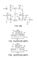
- FIG. 6A is a circuit diagram illustrating a structure of a negative reference voltage generating circuit of Embodiment 9.
- FIG. 6B is a circuit diagram illustrating a structure of a negative reference voltage generating circuit of Embodiment 10.
- FIG. 7B is a vertical cross-sectional view illustrating an NOR flash memory cell of Conventional Example 1, and is a view illustrating a voltage relation required when a Fowler Nordheim programming/erasing operation is performed with a maximum voltage at 10 V.
- FIG. 8 is a circuit diagram illustrating a structure of a negative voltage generating circuit of Conventional Example 2.
- FIG. 9 is a circuit diagram illustrating a structure of a negative voltage generating circuit of Conventional Example 3.
- FIG. 10 is a circuit diagram illustrating a structure example of a negative voltage generating circuit using a negative reference voltage.
- FIG. 1A is a circuit diagram illustrating a structure of a negative reference voltage generating circuit of Embodiment 1.
- the negative reference voltage generating circuit of Embodiment 1 is capable of turning a positive reference voltage PVref into a negative voltage ⁇ PVref by using a switched capacitor circuit and outputting the negative voltage ⁇ PVref as a negative reference voltage NVref.
- the switched capacitor circuit includes four switches SW 1 to SW 4 , two capacitors Cw and Cs, and a clock generating circuit 20 .
- the clock generating circuit 20 generates and outputs a clock CLK and an inverting clock CLKB.
- the clock CLK and the inverting clock CLKB are changed to a high level at different periods.
- the clock generating circuit 20 is omitted in the following drawings.
- an input terminal T 1 is connected to a node n 1 having a node voltage Vn 1 through the switch SW 1 controlled by the clock CLK.
- the node n 1 is grounded through the switch SW 2 controlled by the inverting clock CLKB.
- the capacitor Cw is connected between the node n 1 and a node n 2 having a node voltage Vn 2 .
- the node n 2 is grounded through the switch SW 3 controlled by the clock CLK, and is connected to an output terminal T 2 through the switch SW 4 controlled by the inverting clock CLKB.
- the output terminal T 2 is grounded through the capacitor Cs.
- FIG. 1B is a timing chart illustrating signals of operations of the negative reference voltage generating circuit shown in FIG. 1A .
- the positive reference voltage PVref and 0V i.e., ground voltage
- the nodes n 1 and n 2 at two ends of the capacitor Cw are switched by using the inverting clock CLKB.
- a switched output voltage is maintained by the capacitor Cs and output as the negative reference voltage NVref.
- the negative reference voltage NVref becomes the negative voltage ⁇ PVref.
- the positive reference voltage PVref is applied to the node n 1 in a first period, so as to charge the capacitor Cw.
- a negative voltage is output from the node n 2 based on a voltage charged to the capacitor Cw.
- the negative voltage is output from the second node n 2 as the negative reference voltage NVref by repeating the first period and second period. If the capacitor Cs is sufficiently large and an output current leakage is sufficiently small, a voltage drop of the positive reference voltage PVref and a voltage variation of the output node n 2 may also become sufficiently small. A DC load current does not flow from the negative reference voltage NVref as the output voltage.
- FIG. 2A is a circuit diagram illustrating a structure of a negative reference voltage generating circuit of Embodiment 2.
- FIG. 2B illustrates a level shifter 1 and a level shifter 2 used in the respective embodiments.
- Part (a) in FIG. 2B illustrates a regular inverter 3 that inverts the clock CLK into an inverting clock /CLK.
- Part (b) in FIG. 2B illustrates a regular inverter 4 that inverts the inverting clock CLKB into an inverted inverting clock /CLKB.
- Part (c) in FIG. 2B illustrates the level shifter 1 and the level shifter 2 used in the respective embodiments.
- the level shifter 1 and the level shifter 2 are driven by a positive power voltage Vdd and a negative power voltage ⁇ Vn, and respectively invert the inverting clock /CLK or the inverting clock /CLKB and shift levels, so as to output a clock CLKa or a clock CLKBa.
- the negative reference voltage generating circuit of Embodiment 2 differs from the negative reference voltage generating circuit of Embodiment 1 in the following ways:
- the switch SW 1 is formed by a PMOS transistor T 11 .
- the PMOS transistor T 11 has a substrate tab applied with the positive power voltage Vdd, and controlled by the inverting clock /CLK.
- the switch SW 2 is formed by an NMOS transistor T 12 .
- the NMOS transistor T 12 has a substrate tab that is grounded, and controlled by the inverting clock CLKB.
- the negative reference voltage generating circuit of Embodiment 2 further includes a level shifter 1 .
- the level shifter 1 is driven by the positive power voltage Vdd and a negative power voltage ⁇ Vn 2 such that the inverting clock /CLK is inverted and it's level is shifted, and outputs the clock CLKa having two levels of the positive power voltage Vdd and the negative power voltage ⁇ Vn 2 .
- the negative reference voltage generating circuit of Embodiment 2 further includes the level shifter 2 .
- the level shifter 2 is driven by the positive power voltage Vdd and the negative power voltage NVref such that the inverting clock /CLKB is inverting and it's level is shifted, and outputs the clock CLKBa having two levels of the positive power voltage Vdd and the negative power voltage NVref.
- the switch SW 3 is formed by an NMOS transistor T 21 .
- the node voltage Vn 2 is applied to a substrate tab of the NMOS transistor T 21 that is controlled by the clock CLKa.
- the switch SW 4 is formed by an NMOS transistor T 22 .
- the negative voltage NVref is applied to a substrate tab of the NMOS transistor T 22 that is controlled by the clock CLKBa.
- An issue concerning how to switch the node voltage Vn 2 at the node n 2 may arise when the negative reference voltage generating circuit is formed by the switched capacitor circuit of Embodiment 2. Namely, the node n 2 is switched between 0V and a preset negative voltage, but switching of the negative voltage is unable to be performed by the NMOS transistors T 21 and T 22 that are normally operated between the positive power voltage Vdd and 0V.
- a triple well structure as shown in the following and the level shifters 1 and 2 are required, because a gate also requires a negative voltage when turning off a transistor, so as to make negative voltages of source and drain voltages possible.
- FIG. 2C is a vertical cross-sectional view illustrating a triple well structure of a MOS transistor used in a negative reference voltage generating circuit of FIG. 2A .
- a P-type semiconductor substrate 10 is doped with an N-type dopant, such as phosphorous, to form an N-type well 13 .
- the N-type well 13 is doped with a P+-type dopant to form a P+-type doped region 31 , thereby forming a source.
- the N-type well is doped with a P+-type dopant to form a P+-type doped region 32 , thereby forming a drain.
- the source and the drain are separated by an insulating film, for example, so as to form an electrode 33 , thereby forming a gate.
- an N+-type doped region 34 is formed, thereby forming a substrate tab. Accordingly, the PMOS transistor 11 is formed.
- the P-type semiconductor substrate 10 is doped with an N-type dopant, such as phosphorous, to form a deep N-type well 11 .
- a P-type well 12 is formed by doping into the deep N-type well 11 with a P-type dopant, such as boron, the P-type well 12 is doped with an N+-type dopant to form an N+-type doped region 21 , thereby forming a source, and the P-type well 12 is doped with an N+-type dopant to form an N+-type doped region 22 , thereby forming a drain.
- the source and the drain are separated by an insulating film, for example, so as to form an electrode 23 , thereby forming a gate.
- a P+-type doped region 24 is formed, thereby forming a substrate tab of the P-type well 12 . Accordingly, the NMOS transistors T 21 and T 22 having the triple well structure are formed.
- a P+-type doped region 26 is formed, thereby forming a substrate tab of the P-type semiconductor substrate.
- the NMOS transistors T 21 and T 22 having the triple well structure may be formed accordingly.
- the MOS transistors T 11 to T 22 may replace the switches SW 1 to SW 4 to form the negative reference voltage generating circuit using the switched capacitor circuit. Moreover, based on the negative reference voltage generating circuit, there is no voltage drop of the positive reference voltage PVref, either. In addition, a negative voltage equivalent to an inverting voltage of the positive reference voltage PVref is generated. Thus, the negative reference voltage generating circuit capable of generating the negative reference voltage with a high precision as compared with the conventional art can be provided. Also, a circuit structure of the negative reference voltage generating circuit is simple.
- FIG. 3A is a circuit diagram illustrating a structure of a negative reference voltage generating circuit of Embodiment 3. According to FIG. 3A , the negative reference voltage generating circuit of Embodiment 3 differs from the negative reference voltage generating circuit of Embodiment 2 in the following ways:
- a preset negative voltage (preset negative power voltage) Vnn is applied as the respective negative power voltages of the level shifters 1 and 2 .
- the negative voltage Vnn is a voltage ⁇ Vdd, for example.
- Vdd is the positive power voltage.
- the negative voltage Vnn is applied to the substrate tab of the MOS transistor T 21 .
- the capacitor Cw between the nodes n 1 and n 2 is formed by a capacitor between interconnection wires, for example.
- a negative power terminal of the level shifter 1 is connected to the node n 2 .
- the level shifter 2 also consumes a current from the node NVref.
- the level shifters respectively form parasitic capacitors of the node n 2 and the node NVref.
- the current consumption caused by the parasitic capacitor of the node n 2 and the level shifters 1 and 2 influence an error of the negative reference voltage NVref.
- the parasitic capacitor and the current consumption need to be minimized. Accordingly, as shown in FIG. 3A , by using another negative voltage Vim as the respective negative power voltages of the level shifters 1 and 2 , the parasitic capacitor and the current consumption may be removed.
- FIG. 3C is a timing chart illustrating signals of operations of the negative reference voltage generating circuit shown in FIG. 3A . Also, in an operation example of FIG. 3C , the clock CLKB is a non-overlapping inverting signal of the clock CLK.
- a gate voltage Vg 2 is the negative voltage Vnn.
- the MOS transistor T 22 is turned off, the node voltage Vn 1 is the positive reference voltage PVref, the node voltage Vn 2 is 0V, and the capacitor Cw is being charged.
- the MOS transistor 12 is turned on, and the gate voltage Vg 2 is Vdd.
- the MOS transistor T 22 is turned on.
- the clock CLK is at the low level
- the inverting clock /CLK is at the high level. Therefore, the MOS transistor T 11 is turned off, and the gate voltage Vg 1 is Vnn.
- the MOS transistor T 21 is turned off, the node voltage Vn 1 is 0V, the node voltage Vn 2 becomes ⁇ PVref after a plurality of clock periods and is output as the negative reference voltage NVref.
- the positive reference voltage PVref is converted into the negative voltage ⁇ PVref and output as the negative reference voltage NVref.
- the parasitic capacitor of the node n 2 and the current consumption from the node n 2 and the node NVref may be removed through the simple control operation, thereby suppressing an error of the output voltage.
- the negative voltage that is precisely the inverting voltage of the positive reference voltage PVref is generated, the negative reference voltage generating circuit capable of generating the negative reference voltage with a high precision as compared with the conventional art is provided. Also, a circuit structure of the negative reference voltage generating circuit is simple.
- FIG. 3B is a circuit diagram illustrating a structure of a negative voltage generating circuit of Embodiment 4.
- a negative voltage generating circuit of Embodiment 4 incorporates the circuit that generates the negative voltage Vnn in Embodiment 3.
- the negative voltage generating circuit of Embodiment 4 differs in the following ways:
- the nodes n 1 and n 2 respectively serve as nodes n 3 and n 4 .
- a capacitor Cp is connected between the nodes n 3 and n 4 .
- the capacitor Cp is between the nodes n 3 and n 4 is formed by a capacitor between interconnection wires, for example.
- the negative voltage Vnn is generated at the output terminal T 2 .
- the negative voltage Vnn is applied to the respective negative power voltages of the level shifters 1 and 2 and the substrate tab of the MOS transistor T 21 .
- FIG. 3D is a timing chart illustrating signals of operations of the negative voltage generating circuit shown in FIG. 3B . Also, in an operation example of FIG. 3D , the clock CLKB is a non-overlapping inverting signal of the clock CLK.
- the clock CLK and the clock CLKB are non-overlapping clocks that may be commonly used to generate the negative voltage Vim and the negative reference voltage NVref.
- the clock CLK and the clock CLKB are not required to be the same clock or synchronized clocks.
- the respective high level periods of the clock CLK and the clock CLKB may be generated without being overlapped with each other.
- the clock /CLK and the clock /CLKB are respectively the inverting signals of the clock CLK and the clock CLKB.
- FIG. 3D during the period when the clock CLK is at the high level, the clock /CLK is 0V, and the MOS transistor T 11 is turned on.
- the gate voltage Vg 1 is the voltage Vdd
- the MOS transistor T 21 is turned on.
- the clock CLKB is at a low level
- the MOS transistor T 12 is turned off
- the inverting clock /CLKB is at the high level.
- a gate voltage Vg 2 is the negative voltage Vnn.
- the MOS transistor T 22 is turned off, a node voltage Vn 3 is the voltage Vdd, a node voltage Vn 4 is 0V, and the capacitor Cp is being charged.
- the MOS transistor T 12 is turned on, and the gate voltage Vg 2 is Vdd.
- the MOS transistor T 22 is turned on.
- the clock CLK is at the low level
- the inverting clock /CLK is at the high level. Therefore, the MOS transistor T 11 is turned off, and the gate voltage Vg 1 is Vnn.
- the MOS transistor T 21 is turned off, the node voltage Vn 3 is 0V, the node voltage Vn 4 becomes ⁇ Vdd after a plurality of clock periods and is output as the negative voltage Vnn.
- charges of the capacitor Cp are held separately from the capacitor Cn.
- the positive power voltage Vdd is converted into the negative voltage ⁇ Vdd and output as the negative voltage Vnn.
- a negative voltage that is approximately ⁇ Vdd may be generated by using a circuit substantially the same as the circuit of Embodiment 3 without adjusting a differential amplifying circuit, comparator, etc., of the voltage.
- FIG. 3E is a timing chart illustrating signals of operations when the negative voltage generating circuit of Embodiment 4 is applied to a negative voltage Vim of the negative reference voltage generating circuit of Embodiment 3 shown in FIG. 3A .
- the clock CLK and the clock CLKB are commonly used to generate the negative voltage Vim and the negative reference voltage NVref.
- different clocks such as clocks CLK 1 and CLKB 1 as well as CLK 2 and CLKB 2 , may also be used without problems.
- transistors in Embodiments 3 and 4 are both labeled as transistors T 11 to T 22 , the types of transistors, channel lengths and channel widths are not required to be the same. Namely, the types of transistors, channel lengths and channel widths may be modified based on practical needs.
- FIG. 4A is a circuit diagram illustrating a structure of a negative reference voltage generating circuit of Embodiment 5. According to FIG. 4A , the negative reference voltage generating circuit of Embodiment 5 differs from the negative reference voltage generating circuit of Embodiment 3 in the following way:
- An NMOS transistor T 11 replaces the PMOS transistor T 11 . Moreover, the substrate tab of the NMOS transistor T 11 is grounded.
- a PMOS transistor T 21 replaces the NMOS transistor T 21 . Moreover, the voltage Vdd is applied to the substrate tab of the PMOS transistor T 21 or the substrate tab of the PMOS transistor T 21 is grounded. Also, the clock CLK is applied to the level shifter 1 .
- a PMOS transistor T 22 replaces the NMOS transistor T 22 . Moreover, the voltage Vdd is applied to the substrate tab of the PMOS transistor T 22 or the substrate tab of the PMOS transistor T 22 is grounded. Also, the clock CLKB is applied to the level shifter 2 .
- the PMOS transistors may be replaced with NMOS transistors, and the NMOS transistors may be replaced with PMOS transistors, depending on the power voltage Vdd, the positive reference voltage PVref, and a threshold voltage Vth of the MOS transistors.
- Vdd the power voltage
- PVref the positive reference voltage
- Vth a threshold voltage of the MOS transistors.
- an operation may be performed when Vdd ⁇ 2.5 V, PVref ⁇ 1.2 V, and Vth ⁇ 0.8 V. Since a high level voltage Vdd of the clock CLK is greater than PVref+Vth, the MOS transistor T 11 may allow the positive reference voltage PVref to pass.
- the MOS transistor T 12 when the MOS transistor T 12 allows the voltage of 0V to pass, the MOS transistor T 12 has to be an NMOS transistor. If the MOS transistor T 12 is a PMOS transistor, since the voltage is unable to pass during a turn-on period when the gate voltage is 0V, the negative reference voltage generating circuit is unable to generate an accurate reference voltage.
- FIG. 4B is a circuit diagram illustrating a structure of a negative voltage generating circuit of Embodiment 6. According to FIG. 4B , the negative voltage generating circuit of Embodiment 6 differs from the negative generating circuit of Embodiment 4 in the following way.
- a PMOS transistor T 21 replaces the NMOS transistor T 21 . Moreover, the voltage Vdd is applied to the substrate tab of the PMOS transistor T 21 . Also, the clock CLK is applied to the level shifter 1 .
- the MOS transistor T 22 is not changed into a PMOS transistor in this embodiment, because if the clock CLKB is at the high level and the node n 4 has a negative voltage, a drain of the PMOS transistor T 22 is set as Vn 4 , a source thereof is set as Vim, and a gate thereof is set as Vim, the negative voltage of the node n 4 is unable to be transmitted to the node T 2 as Vn 4 ⁇ Vnn and the PMOS transistor T 22 is turned off.
- FIG. 4C is a timing chart illustrating signals of operations of the negative reference voltage generating circuit shown in FIG. 4A in combination with the negative voltage generating circuit shown in FIG. 4B . Except for the following, the negative reference voltage generating circuit shown in FIG. 4A and the negative voltage generating circuit shown in FIG. 4B operate in the same way as Embodiments 3 and 4.
- the node voltage Vn 4 is increased up to
- Vth PMOS transistor
- the negative voltage Vim is still at 0V
- the gate voltage Vg 1 is equal to 0V
- a source voltage of the MOS transistor T 21 is 0V.
- the node voltage Vn 4 as the drain voltage merely drops by the threshold voltage
- is charged to the capacitor Cp. Therefore, the voltage may successfully drop to 0V after a plurality of clock periods by using the negative voltage Vim.
- the positive power voltage Vdd is converted into the negative voltage Vim, and the positive reference voltage PVref is converted into the negative reference voltage NVref and output.
- the parasitic capacitor of the node n 2 and the current consumption from the node n 2 and the node NVref may be removed through the simple control operation, thereby suppressing the error of the output voltage. Also, since the negative voltage that is precisely the inverting voltage of the positive reference voltage PVref is generated, the negative reference voltage generating circuit capable of generating the negative reference voltage with a high precision as compared with the conventional art is provided with a simple circuit structure of the negative reference voltage generating circuit.
- FIG. 4D is a circuit diagram illustrating Structure Example 1 of a negative reference voltage generating circuit of Embodiment 7.
- the negative reference voltage generating circuit of the Embodiment 7 replaces the PMOS transistor T 11 in Embodiment 2 with the NMOS transistor T 11 (Embodiment 5).
- the structure and operation of Embodiment 7 are the same as Embodiments 2 and 5.
- FIG. 4E is a circuit diagram illustrating Structure Example 2 of a negative reference voltage generating circuit of Embodiment 7, where the PMOS transistor T 11 in the negative reference voltage generating circuit of Embodiment 3 of FIG. 3A is replaced by the NMOS transistor T 11 (Embodiment 5 of FIG. 4A ), and the substrate tab of the NMOS transistor T 22 is connected to the negative voltage Vim.
- Embodiment 8 structure examples of the capacitors Cw and Cp used in Embodiments 1 to 7 are described.
- the capacitors are required to keep capacitance values constant whether the clock CLK or CLKB is at the high level or low level. Otherwise, the voltage may change when the voltage is inverted.
- capacitors between interconnection wires that are metal-oxide-metal (MOM) capacitors should be used.
- MOM metal-oxide-metal
- FIG. 5A is a vertical cross-sectional view illustrating a structure of a capacitor of Structure Example 1 used in Embodiments 1 to 7.
- FIG. 5A illustrates a structure example of a MOS capacitor formed between a gate doped N+-type dopant and a P-well.
- the P-type semiconductor substrate 10 is doped with an N-type dopant, such as phosphorous, to form a deep N-type well 11 .
- the deep N-type well 11 is doped with a P-type dopant, such as boron, to form the P-type well 12 .
- Two parts of the P-type well 12 are doped with P+-type dopants to form P+-type doped regions 41 and 42 , thereby forming two electrode tabs.
- the electrode tabs are connected to the node n 1 .
- an electrode 43 is formed with separation of an insulating layer.
- the electrode 43 is connected to the node n 2 .
- the deep N-type well 11 is doped with an N+-type dopant to form an N+-type doped region 44 serving as a substrate tab.
- the P-type semiconductor substrate 10 is doped with a P+-type dopant to form a P+-type doped region 45 serving as a substrate tab to be rounded.
- a capacitor C may be formed between the nodes n 1 and n 2 . Whether the clock CLK or the clock CLKB is at the high or low level, the node n 1 is at the high level, and the node T 12 is at the low level. Thus, the MOS capacitor is kept at an accumulation state, and the capacitance may be kept constant.
- FIG. 5B is a vertical cross-sectional view illustrating a structure of a capacitor of Structure Example 2 used in Embodiments 1 to 7.
- FIG. 5B illustrates a structure example of a capacitor in a channel of a gate, a source, and a drain formed by a PMOS transistor.
- the P-type semiconductor substrate 10 is doped with an N-type dopant, such as boron, to form the N-type well 13 .
- Two parts of the N-type well 13 are doped with P+-type dopants to form P+-type doped regions 51 and 52 , thereby forming the source and the drain. Then, the P+-type doped regions 51 and 52 are connected to the node n 1 .
- a gate 53 is formed with separation of an insulating layer.
- the gate 53 is connected to the node n 2 .
- the N-type well 13 is doped with an N+-type dopant to form an N+-type doped region 54 serving as a substrate tab.
- the P-type semiconductor substrate 10 is doped with a P+-type dopant to form a P+-type doped region 55 serving as a substrate tab to be grounded.
- the capacitor C may be formed between the nodes n 1 and n 2 .
- the node n 1 is at the high level, and the node n 2 is at the low level.
- the PMOS transistor is kept at a turn-on state, and the capacitance may be kept constant.
- FIG. 5D is a vertical cross-sectional view illustrating a structure of Structure Example 4 of a capacitor of Embodiment 7 used in Embodiments 1 to 7.
- the MOS transistor of FIG. 5B may be formed in FIG. 5C by combining the structures of FIGS. 5B and 5C like FIG. 5D (However, the channel is different.). Namely, an N+-type doped region 61 A and an N+-type doped region 66 are formed at two sides of a gate as a source and a drain. Then, the source and the drain are connected to the node n 1 .
- FIG. 5D is a vertical cross-sectional view illustrating a structure of Structure Example 4 of a capacitor of Embodiment 7 used in Embodiments 1 to 7.
- the MOS transistor of FIG. 5B may be formed in FIG. 5C by combining the structures of FIGS. 5B and 5C like FIG. 5D (However, the channel is different.). Namely, an N+-type doped region
- the MOS transistor includes the stacked floating gate 62 and control gate 63
- the floating gate 62 may also be connected to the node n 1
- the control gate 63 may be connected to the node n 2 , so as to form a capacitor between the floating gate 62 and the control gate 63 .
- the capacitors Cw and Cp used in Embodiments 1 to 7 may be forming according to any one of the structures shown in FIGS. 5A, 5B, 5C, and 5D .
- the capacitors C operate for Vn 1 >Vn 2 .
- the capacitor C may also be formed between two electrodes.
- the output negative reference voltage NVref may be influenced by the parasitic capacitor of the node n 2 .
- the parasitic capacitor should be suppressed as much as possible.
- a capacitance to the substrate of the drain (node n 2 ) of the MOS transistor T 21 and the MOS transistor T 22 is the main parasitic capacitor.
- NVref is the negative reference voltage
- the negative reference voltage NVref needs to be constant and to suppress ripple noises.
- the ripple noises may be suppressed by disposing the RC filter at the output end.
- ripple noises generated by driving the MOS transistor T 22 may be suppressed.
- Embodiment 9 is configured by adding the RC low pass filter 5 to Embodiment 3, the RC low pass filter 5 may also be added to Embodiments 1, 2, and 4 to 8.
- FIG. 6B is a circuit diagram illustrating a structure of a negative reference voltage generating circuit of Embodiment 10.
- the negative reference voltage generating circuit of Embodiment 10 includes: the output terminal T 2 of the negative reference voltage generating circuit of Embodiment 3 has additionally an RC low pass filter 5 A having the serial resistor R and a parallel capacitor Cs (formed by connecting the original capacitor Cs to the output terminal T 2 side of the serial resistor R).
- the negative reference voltage generating circuit achieves particular efficacies as follows: compared with the conventional art, the negative reference voltage may be generated at a high precision according to the variation of temperature, and the circuit structure thereof is simple.
- the clocks CLK, /CLK, CLKB, and /CLKB are used to control whether the switches SW 1 to SW 4 and the MOS transistors T 11 to T 22 are turned on or off.
- the invention is not limited thereto. Preset control signals may also be respectively used.
- the negative reference voltage generating circuit is capable of providing the negative reference voltage generating circuit and the negative reference voltage generating system that generate the negative reference voltage at a high precision compared with the prior art, and the circuit structure thereof is simple.
- the negative reference voltage generating circuit and the negative reference voltage generating system according to the invention may be applied to a non-volatile memory device, such as NOR flash memory, or a dynamic random access memory (DRAM), etc.
Abstract
Description
- [Patent Document 1] Specification of US Publication No. 2012/0218032.
- [Patent Document 2] JP Patent Publication No. 2009-016929.
- [Patent Document 3] JP Patent Publication No. 2009-074973.
- [Patent Document 4] Specification of US Publication No. 2008/0018318.
- [Patent Document 5] JP Patent Publication No. H10-239357.
- [Patent Document 6] JP Patent Publication No. 2000-339047.
- [Patent Document 7] JP Patent Publication No. 2002-367374.
- [Patent Document 8] Specification of US Publication No. 2012/155168.
- [Patent Document 9] International Publication No. WO2006/025099.
- [Patent Document 10] JP Patent Publication No. 2004-350290.
- [Non-Patent Document 1] Comel Stanescu et al., “High PSRR CMOS Voltage Reference for Negative IDOS”, Proceedings of 2004 International Semiconductor Conference (CAS 2004), 27th Edition, Oct. 4-6, 2004, in Sinaia, Romania.
- [Non-Patent Document 2] Oguey et al., “MOS Voltage Reference Based on Polysilicon Gate Work Function Difference”, IEEE Journal of Solid-State Circuits, Vol. SC-15, No. 3, June 1980.
Vneg=−R22/R21×Vpp+(1+R22/R21)×PVref (1)
Vneg=−Iref×R32+PVref (2)
Iref=PVref/R31 (3)
Vneg=(R42/R41+1)×NVref (4)
NVref=−Iref×R52 (5)
NVref=−PVref×R62/R61 (6)
Claims (16)
Applications Claiming Priority (2)
| Application Number | Priority Date | Filing Date | Title |
|---|---|---|---|
| JP2015-007715 | 2015-01-19 | ||
| JP2015007715A JP5911614B1 (en) | 2015-01-19 | 2015-01-19 | Negative reference voltage generator |
Publications (2)
| Publication Number | Publication Date |
|---|---|
| US20160211744A1 US20160211744A1 (en) | 2016-07-21 |
| US9502969B2 true US9502969B2 (en) | 2016-11-22 |
Family
ID=55808263
Family Applications (1)
| Application Number | Title | Priority Date | Filing Date |
|---|---|---|---|
| US14/819,452 Active US9502969B2 (en) | 2015-01-19 | 2015-08-06 | Negative reference voltage generating circuit |
Country Status (4)
| Country | Link |
|---|---|
| US (1) | US9502969B2 (en) |
| JP (1) | JP5911614B1 (en) |
| CN (1) | CN105807835B (en) |
| TW (1) | TWI559114B (en) |
Cited By (2)
| Publication number | Priority date | Publication date | Assignee | Title |
|---|---|---|---|---|
| US20170060217A1 (en) * | 2012-09-03 | 2017-03-02 | Semiconductor Energy Laboratory Co., Ltd. | Semiconductor Device and Electronic Device |
| US20190044438A1 (en) * | 2016-04-01 | 2019-02-07 | Tdk Corporation | Negative charge pump and audio asic with such negative charge pump |
Families Citing this family (13)
| Publication number | Priority date | Publication date | Assignee | Title |
|---|---|---|---|---|
| US9755507B2 (en) * | 2015-12-03 | 2017-09-05 | Mediatek Inc. | Reference voltage generator having at least one bipolar junction transistor biased by negative base voltage and associated reference voltage generating method |
| US10044449B2 (en) * | 2016-07-04 | 2018-08-07 | Electronics And Telecommunications Research Institute | Reception device and transmission/reception system including the same |
| JP6805798B2 (en) * | 2016-12-19 | 2020-12-23 | セイコーエプソン株式会社 | Overcurrent detection circuit, semiconductor device, and power supply device |
| CN109889033A (en) * | 2017-05-22 | 2019-06-14 | 南京矽力杰半导体技术有限公司 | Isolated form Switching capacitors |
| CN107493012B (en) * | 2017-07-17 | 2019-08-13 | 上海华虹宏力半导体制造有限公司 | Negative pressure charge pump |
| CN107968552B (en) * | 2017-12-29 | 2020-01-03 | 电子科技大学 | Floating gate voltage driving circuit for switch power supply |
| CN110348432A (en) * | 2018-04-01 | 2019-10-18 | 印芯科技股份有限公司 | Optical recognition module |
| JP6952644B2 (en) * | 2018-05-14 | 2021-10-20 | 株式会社東芝 | Semiconductor integrated circuit |
| CN111181394B (en) * | 2018-11-12 | 2021-05-07 | 台达电子企业管理(上海)有限公司 | Switch resonant cavity direct current converter and transformation ratio switching method thereof |
| CN110601511B (en) * | 2019-08-22 | 2020-11-24 | 敦泰电子(深圳)有限公司 | Gate drive circuit, charge pump with gate drive circuit and chip |
| CN111124032B (en) * | 2019-12-20 | 2021-11-05 | 睿兴科技(南京)有限公司 | Filter circuit for suppressing noise interference and micro control system |
| CN112416043A (en) * | 2020-11-27 | 2021-02-26 | 敦泰电子(深圳)有限公司 | Negative voltage generating circuit and chip |
| CN113708747B (en) * | 2021-10-28 | 2022-02-08 | 广州慧智微电子股份有限公司 | Controlled switch switching circuit and switching device |
Citations (19)
| Publication number | Priority date | Publication date | Assignee | Title |
|---|---|---|---|---|
| JPH10239357A (en) | 1997-02-26 | 1998-09-11 | Toshiba Corp | Negative voltage detection circuit and nonvolatile semiconductor memory device |
| JP2000339047A (en) | 1999-05-27 | 2000-12-08 | Hitachi Ltd | Semiconductor integrated circuit device |
| TW510076B (en) | 1998-09-25 | 2002-11-11 | Intel Corp | A scaleable charge pump for use with a low voltage power supply |
| JP2002367374A (en) | 2001-06-11 | 2002-12-20 | Hitachi Ltd | Negative voltage generating circuit and semiconductor memory |
| US20030151448A1 (en) * | 2002-02-12 | 2003-08-14 | Toshiya Fujiyama | Negative voltage output charge pump circuit |
| JP2004350290A (en) | 2003-05-20 | 2004-12-09 | Toshiba Corp | Band gap voltage reference generator circuit, thermal sensing circuit, and integrated circuit |
| WO2006025099A1 (en) | 2004-08-31 | 2006-03-09 | Spansion Llc | Nonvolatile storage device and control method thereof |
| CN101088211A (en) | 2004-12-28 | 2007-12-12 | 罗姆股份有限公司 | Power supply circuit, charge pump circuit, and portable appliance therewith |
| US20080018318A1 (en) | 2006-07-18 | 2008-01-24 | Etron Technology, Inc. | Negative voltage generator |
| JP2009016929A (en) | 2007-06-29 | 2009-01-22 | Toshiba Corp | Negative voltage detection circuit, and semiconductor integrated circuit employing the same |
| JP2009074973A (en) | 2007-09-21 | 2009-04-09 | Toshiba Corp | Negative voltage detection circuit and semiconductor integrated circuit including negative voltage detection circuit |
| JP2009081984A (en) | 2007-09-04 | 2009-04-16 | Panasonic Corp | Charge pump circuit |
| CN100592153C (en) | 2007-06-08 | 2010-02-24 | 群康科技(深圳)有限公司 | Negative voltage generation circuit |
| CN102195471A (en) | 2010-03-09 | 2011-09-21 | 曜鹏亿发(北京)科技有限公司 | Negative-pressure output charge pump circuit |
| US20120155168A1 (en) | 2010-12-20 | 2012-06-21 | Samsung Electronics Co., Ltd. | Negative voltage generator, decoder, nonvolatile memory device and memory system using negative voltage |
| CN102640405A (en) | 2010-11-12 | 2012-08-15 | 旭化成微电子株式会社 | Charge pump circuit, method for controlling same, and semiconductor integrated circuit |
| US20120218032A1 (en) | 2011-02-24 | 2012-08-30 | Rf Micro Devices, Inc. | High efficiency negative regulated charge-pump |
| US20150070085A1 (en) * | 2013-09-10 | 2015-03-12 | Dialog Semiconductor Gmbh | Reduction in on-resistance in pass device |
| US20160126830A1 (en) * | 2014-10-30 | 2016-05-05 | Mediatek Singapore Pte. Ltd. | Charge pump circuit, integrated circuit, electronic device and method therefor |
Family Cites Families (4)
| Publication number | Priority date | Publication date | Assignee | Title |
|---|---|---|---|---|
| JP3723445B2 (en) * | 1999-12-27 | 2005-12-07 | 三洋電機株式会社 | Voltage generation circuit and display device including voltage generation circuit |
| TW486869B (en) * | 1999-12-27 | 2002-05-11 | Sanyo Electric Co | Voltage producing circuit and a display device provided with such voltage producing circuit |
| JP2013172482A (en) * | 2012-02-17 | 2013-09-02 | Toshiba Corp | Switch control circuit, semiconductor device, and radio communication equipment |
| US9111601B2 (en) * | 2012-06-08 | 2015-08-18 | Qualcomm Incorporated | Negative voltage generators |
-
2015
- 2015-01-19 JP JP2015007715A patent/JP5911614B1/en active Active
- 2015-08-06 US US14/819,452 patent/US9502969B2/en active Active
- 2015-08-18 TW TW104126838A patent/TWI559114B/en active
- 2015-08-27 CN CN201510534068.2A patent/CN105807835B/en active Active
Patent Citations (19)
| Publication number | Priority date | Publication date | Assignee | Title |
|---|---|---|---|---|
| JPH10239357A (en) | 1997-02-26 | 1998-09-11 | Toshiba Corp | Negative voltage detection circuit and nonvolatile semiconductor memory device |
| TW510076B (en) | 1998-09-25 | 2002-11-11 | Intel Corp | A scaleable charge pump for use with a low voltage power supply |
| JP2000339047A (en) | 1999-05-27 | 2000-12-08 | Hitachi Ltd | Semiconductor integrated circuit device |
| JP2002367374A (en) | 2001-06-11 | 2002-12-20 | Hitachi Ltd | Negative voltage generating circuit and semiconductor memory |
| US20030151448A1 (en) * | 2002-02-12 | 2003-08-14 | Toshiya Fujiyama | Negative voltage output charge pump circuit |
| JP2004350290A (en) | 2003-05-20 | 2004-12-09 | Toshiba Corp | Band gap voltage reference generator circuit, thermal sensing circuit, and integrated circuit |
| WO2006025099A1 (en) | 2004-08-31 | 2006-03-09 | Spansion Llc | Nonvolatile storage device and control method thereof |
| CN101088211A (en) | 2004-12-28 | 2007-12-12 | 罗姆股份有限公司 | Power supply circuit, charge pump circuit, and portable appliance therewith |
| US20080018318A1 (en) | 2006-07-18 | 2008-01-24 | Etron Technology, Inc. | Negative voltage generator |
| CN100592153C (en) | 2007-06-08 | 2010-02-24 | 群康科技(深圳)有限公司 | Negative voltage generation circuit |
| JP2009016929A (en) | 2007-06-29 | 2009-01-22 | Toshiba Corp | Negative voltage detection circuit, and semiconductor integrated circuit employing the same |
| JP2009081984A (en) | 2007-09-04 | 2009-04-16 | Panasonic Corp | Charge pump circuit |
| JP2009074973A (en) | 2007-09-21 | 2009-04-09 | Toshiba Corp | Negative voltage detection circuit and semiconductor integrated circuit including negative voltage detection circuit |
| CN102195471A (en) | 2010-03-09 | 2011-09-21 | 曜鹏亿发(北京)科技有限公司 | Negative-pressure output charge pump circuit |
| CN102640405A (en) | 2010-11-12 | 2012-08-15 | 旭化成微电子株式会社 | Charge pump circuit, method for controlling same, and semiconductor integrated circuit |
| US20120155168A1 (en) | 2010-12-20 | 2012-06-21 | Samsung Electronics Co., Ltd. | Negative voltage generator, decoder, nonvolatile memory device and memory system using negative voltage |
| US20120218032A1 (en) | 2011-02-24 | 2012-08-30 | Rf Micro Devices, Inc. | High efficiency negative regulated charge-pump |
| US20150070085A1 (en) * | 2013-09-10 | 2015-03-12 | Dialog Semiconductor Gmbh | Reduction in on-resistance in pass device |
| US20160126830A1 (en) * | 2014-10-30 | 2016-05-05 | Mediatek Singapore Pte. Ltd. | Charge pump circuit, integrated circuit, electronic device and method therefor |
Non-Patent Citations (2)
| Title |
|---|
| Oguey et al, "MOS Voltage Reference Based on Polysilicon Gate Work Function Difference", IEEE Journal of Solid-State Circuits, vol. SC-15, No. 3, Jun. 1980, pp. 264-269. |
| Stanescu et al,"High PSRR CMOS Voltage Reference for Negative IDOS", Proceedings of 2004 International Semiconductor Conference (CAS 2004), 27th Edition, Oct. 4-6, 2004, in Sinaia, Romania, pp. 311-314. |
Cited By (4)
| Publication number | Priority date | Publication date | Assignee | Title |
|---|---|---|---|---|
| US20170060217A1 (en) * | 2012-09-03 | 2017-03-02 | Semiconductor Energy Laboratory Co., Ltd. | Semiconductor Device and Electronic Device |
| US9825526B2 (en) * | 2012-09-03 | 2017-11-21 | Semiconductor Energy Laboratory Co., Ltd. | Semiconductor device and electronic device |
| US20190044438A1 (en) * | 2016-04-01 | 2019-02-07 | Tdk Corporation | Negative charge pump and audio asic with such negative charge pump |
| US10630173B2 (en) * | 2016-04-01 | 2020-04-21 | Tdk Corporation | Negative charge pump and audio ASIC with such negative charge pump |
Also Published As
| Publication number | Publication date |
|---|---|
| CN105807835A (en) | 2016-07-27 |
| TWI559114B (en) | 2016-11-21 |
| CN105807835B (en) | 2017-09-15 |
| JP5911614B1 (en) | 2016-04-27 |
| TW201627792A (en) | 2016-08-01 |
| JP2016134989A (en) | 2016-07-25 |
| US20160211744A1 (en) | 2016-07-21 |
Similar Documents
| Publication | Publication Date | Title |
|---|---|---|
| US9502969B2 (en) | Negative reference voltage generating circuit | |
| US6351179B1 (en) | Semiconductor integrated circuit having active mode and standby mode converters | |
| US9397562B1 (en) | Negative reference voltage generating circuit and system thereof | |
| JP4851903B2 (en) | Semiconductor charge pump | |
| US7932770B2 (en) | Charge pump circuit | |
| US20070122964A1 (en) | Semiconductor Device Equipped with a Voltage Step-Up Circuit | |
| US20080315246A1 (en) | Transistor switch circuit and sample-and-hold circuit | |
| JPH1131950A (en) | Level shift circuit | |
| KR100532765B1 (en) | Semiconductor memory device | |
| US9285821B2 (en) | Negative reference voltage generating circuit and negative reference voltage generating system using the same | |
| JP3680122B2 (en) | Reference voltage generation circuit | |
| EP1349264B1 (en) | Basic stage for a charge pump circuit | |
| KR20190096269A (en) | Reference voltage circuit and semiconductor device | |
| US9646992B2 (en) | Semiconductor memory | |
| US9360877B2 (en) | Negative voltage regulation circuit and voltage generation circuit including the same | |
| US7808303B2 (en) | Booster circuit | |
| US11929434B2 (en) | High voltage switch device | |
| Racape et al. | A PMOS-switch based charge pump, allowing lost cost implementation on a CMOS standard process | |
| JPH09266281A (en) | Step-up circuit | |
| JP2016187123A (en) | Comparator circuit | |
| JP2000105611A (en) | Charge pump circuit | |
| JP2000163970A (en) | Back-bias circuit | |
| US20230155498A1 (en) | Current source circuit | |
| JP2003051550A (en) | Semiconductor device | |
| KR20000060386A (en) | Substrate bias generator circuit of memory device |
Legal Events
| Date | Code | Title | Description |
|---|---|---|---|
| AS | Assignment |
Owner name: POWERCHIP TECHNOLOGY CORPORATION, TAIWAN Free format text: ASSIGNMENT OF ASSIGNORS INTEREST;ASSIGNORS:ARAKAWA, HIDEKI;KITANI, TOMOFUMI;SIGNING DATES FROM 20150608 TO 20150629;REEL/FRAME:036302/0960 |
|
| STCF | Information on status: patent grant |
Free format text: PATENTED CASE |
|
| AS | Assignment |
Owner name: POWERCHIP SEMICONDUCTOR MANUFACTURING CORPORATION, Free format text: ASSIGNMENT OF ASSIGNORS INTEREST;ASSIGNOR:POWERCHIP TECHNOLOGY CORPORATION;REEL/FRAME:049770/0171 Effective date: 20190628 |
|
| MAFP | Maintenance fee payment |
Free format text: PAYMENT OF MAINTENANCE FEE, 4TH YEAR, LARGE ENTITY (ORIGINAL EVENT CODE: M1551); ENTITY STATUS OF PATENT OWNER: LARGE ENTITY Year of fee payment: 4 |