US9412295B2 - Pixel circuit and driving method thereof - Google Patents
Pixel circuit and driving method thereof Download PDFInfo
- Publication number
- US9412295B2 US9412295B2 US14/269,439 US201414269439A US9412295B2 US 9412295 B2 US9412295 B2 US 9412295B2 US 201414269439 A US201414269439 A US 201414269439A US 9412295 B2 US9412295 B2 US 9412295B2
- Authority
- US
- United States
- Prior art keywords
- transistor
- pixel circuit
- light emitting
- supplied
- gray scale
- Prior art date
- Legal status (The legal status is an assumption and is not a legal conclusion. Google has not performed a legal analysis and makes no representation as to the accuracy of the status listed.)
- Active, expires
Links
- 238000000034 method Methods 0.000 title claims description 18
- 238000010586 diagram Methods 0.000 description 30
- 238000006243 chemical reaction Methods 0.000 description 17
- 230000007704 transition Effects 0.000 description 6
- 239000003990 capacitor Substances 0.000 description 5
- 238000011017 operating method Methods 0.000 description 4
- 230000000052 comparative effect Effects 0.000 description 3
- 230000003071 parasitic effect Effects 0.000 description 3
- 230000000750 progressive effect Effects 0.000 description 2
- 239000013256 coordination polymer Substances 0.000 description 1
- 230000000694 effects Effects 0.000 description 1
- 239000004973 liquid crystal related substance Substances 0.000 description 1
- 239000011159 matrix material Substances 0.000 description 1
- 230000003287 optical effect Effects 0.000 description 1
- 230000001629 suppression Effects 0.000 description 1
Images


Classifications
-
- G—PHYSICS
- G09—EDUCATION; CRYPTOGRAPHY; DISPLAY; ADVERTISING; SEALS
- G09G—ARRANGEMENTS OR CIRCUITS FOR CONTROL OF INDICATING DEVICES USING STATIC MEANS TO PRESENT VARIABLE INFORMATION
- G09G3/00—Control arrangements or circuits, of interest only in connection with visual indicators other than cathode-ray tubes
- G09G3/20—Control arrangements or circuits, of interest only in connection with visual indicators other than cathode-ray tubes for presentation of an assembly of a number of characters, e.g. a page, by composing the assembly by combination of individual elements arranged in a matrix no fixed position being assigned to or needed to be assigned to the individual characters or partial characters
- G09G3/22—Control arrangements or circuits, of interest only in connection with visual indicators other than cathode-ray tubes for presentation of an assembly of a number of characters, e.g. a page, by composing the assembly by combination of individual elements arranged in a matrix no fixed position being assigned to or needed to be assigned to the individual characters or partial characters using controlled light sources
- G09G3/30—Control arrangements or circuits, of interest only in connection with visual indicators other than cathode-ray tubes for presentation of an assembly of a number of characters, e.g. a page, by composing the assembly by combination of individual elements arranged in a matrix no fixed position being assigned to or needed to be assigned to the individual characters or partial characters using controlled light sources using electroluminescent panels
- G09G3/32—Control arrangements or circuits, of interest only in connection with visual indicators other than cathode-ray tubes for presentation of an assembly of a number of characters, e.g. a page, by composing the assembly by combination of individual elements arranged in a matrix no fixed position being assigned to or needed to be assigned to the individual characters or partial characters using controlled light sources using electroluminescent panels semiconductive, e.g. using light-emitting diodes [LED]
- G09G3/3208—Control arrangements or circuits, of interest only in connection with visual indicators other than cathode-ray tubes for presentation of an assembly of a number of characters, e.g. a page, by composing the assembly by combination of individual elements arranged in a matrix no fixed position being assigned to or needed to be assigned to the individual characters or partial characters using controlled light sources using electroluminescent panels semiconductive, e.g. using light-emitting diodes [LED] organic, e.g. using organic light-emitting diodes [OLED]
- G09G3/3225—Control arrangements or circuits, of interest only in connection with visual indicators other than cathode-ray tubes for presentation of an assembly of a number of characters, e.g. a page, by composing the assembly by combination of individual elements arranged in a matrix no fixed position being assigned to or needed to be assigned to the individual characters or partial characters using controlled light sources using electroluminescent panels semiconductive, e.g. using light-emitting diodes [LED] organic, e.g. using organic light-emitting diodes [OLED] using an active matrix
- G09G3/3233—Control arrangements or circuits, of interest only in connection with visual indicators other than cathode-ray tubes for presentation of an assembly of a number of characters, e.g. a page, by composing the assembly by combination of individual elements arranged in a matrix no fixed position being assigned to or needed to be assigned to the individual characters or partial characters using controlled light sources using electroluminescent panels semiconductive, e.g. using light-emitting diodes [LED] organic, e.g. using organic light-emitting diodes [OLED] using an active matrix with pixel circuitry controlling the current through the light-emitting element
-
- G—PHYSICS
- G09—EDUCATION; CRYPTOGRAPHY; DISPLAY; ADVERTISING; SEALS
- G09G—ARRANGEMENTS OR CIRCUITS FOR CONTROL OF INDICATING DEVICES USING STATIC MEANS TO PRESENT VARIABLE INFORMATION
- G09G3/00—Control arrangements or circuits, of interest only in connection with visual indicators other than cathode-ray tubes
- G09G3/20—Control arrangements or circuits, of interest only in connection with visual indicators other than cathode-ray tubes for presentation of an assembly of a number of characters, e.g. a page, by composing the assembly by combination of individual elements arranged in a matrix no fixed position being assigned to or needed to be assigned to the individual characters or partial characters
- G09G3/22—Control arrangements or circuits, of interest only in connection with visual indicators other than cathode-ray tubes for presentation of an assembly of a number of characters, e.g. a page, by composing the assembly by combination of individual elements arranged in a matrix no fixed position being assigned to or needed to be assigned to the individual characters or partial characters using controlled light sources
- G09G3/30—Control arrangements or circuits, of interest only in connection with visual indicators other than cathode-ray tubes for presentation of an assembly of a number of characters, e.g. a page, by composing the assembly by combination of individual elements arranged in a matrix no fixed position being assigned to or needed to be assigned to the individual characters or partial characters using controlled light sources using electroluminescent panels
- G09G3/32—Control arrangements or circuits, of interest only in connection with visual indicators other than cathode-ray tubes for presentation of an assembly of a number of characters, e.g. a page, by composing the assembly by combination of individual elements arranged in a matrix no fixed position being assigned to or needed to be assigned to the individual characters or partial characters using controlled light sources using electroluminescent panels semiconductive, e.g. using light-emitting diodes [LED]
- G09G3/3208—Control arrangements or circuits, of interest only in connection with visual indicators other than cathode-ray tubes for presentation of an assembly of a number of characters, e.g. a page, by composing the assembly by combination of individual elements arranged in a matrix no fixed position being assigned to or needed to be assigned to the individual characters or partial characters using controlled light sources using electroluminescent panels semiconductive, e.g. using light-emitting diodes [LED] organic, e.g. using organic light-emitting diodes [OLED]
- G09G3/3275—Details of drivers for data electrodes
- G09G3/3291—Details of drivers for data electrodes in which the data driver supplies a variable data voltage for setting the current through, or the voltage across, the light-emitting elements
-
- G—PHYSICS
- G09—EDUCATION; CRYPTOGRAPHY; DISPLAY; ADVERTISING; SEALS
- G09G—ARRANGEMENTS OR CIRCUITS FOR CONTROL OF INDICATING DEVICES USING STATIC MEANS TO PRESENT VARIABLE INFORMATION
- G09G2300/00—Aspects of the constitution of display devices
- G09G2300/08—Active matrix structure, i.e. with use of active elements, inclusive of non-linear two terminal elements, in the pixels together with light emitting or modulating elements
- G09G2300/0809—Several active elements per pixel in active matrix panels
- G09G2300/0842—Several active elements per pixel in active matrix panels forming a memory circuit, e.g. a dynamic memory with one capacitor
- G09G2300/0861—Several active elements per pixel in active matrix panels forming a memory circuit, e.g. a dynamic memory with one capacitor with additional control of the display period without amending the charge stored in a pixel memory, e.g. by means of additional select electrodes
-
- G—PHYSICS
- G09—EDUCATION; CRYPTOGRAPHY; DISPLAY; ADVERTISING; SEALS
- G09G—ARRANGEMENTS OR CIRCUITS FOR CONTROL OF INDICATING DEVICES USING STATIC MEANS TO PRESENT VARIABLE INFORMATION
- G09G2310/00—Command of the display device
- G09G2310/02—Addressing, scanning or driving the display screen or processing steps related thereto
- G09G2310/0243—Details of the generation of driving signals
- G09G2310/0251—Precharge or discharge of pixel before applying new pixel voltage
-
- G—PHYSICS
- G09—EDUCATION; CRYPTOGRAPHY; DISPLAY; ADVERTISING; SEALS
- G09G—ARRANGEMENTS OR CIRCUITS FOR CONTROL OF INDICATING DEVICES USING STATIC MEANS TO PRESENT VARIABLE INFORMATION
- G09G2310/00—Command of the display device
- G09G2310/02—Addressing, scanning or driving the display screen or processing steps related thereto
- G09G2310/0262—The addressing of the pixel, in a display other than an active matrix LCD, involving the control of two or more scan electrodes or two or more data electrodes, e.g. pixel voltage dependent on signals of two data electrodes
Definitions
- Embodiments described herein relate to an electrical optical device, and more particularly, relate to a pixel circuit and a method of driving the pixel circuit.
- display devices replacing CRT (Cathode Ray Tube) displays include organic EL devices that have self-emissive elements.
- the organic EL device may be used as a backlight for a liquid crystal display (LCD) device or as an organic EL display device.
- the organic EL display device has attracted attention.
- a gray scale to be expressed is realized by controlling a driving transistor of each pixel circuit and the amount of current supplied to a light emitting diode thereof. If a characteristic of the driving transistor varies, the gray scale expression varies; hence, the quality of display is lowered.
- a threshold voltage compensation technique which suppresses a variation in a threshold voltage (Vth) of a transistor.
- a threshold voltage compensation circuit controls the amount of current to be supplied to a light emitting element using input image data, without depending on a variation in a threshold voltage of a driving transistor.
- it is possible to compensate for a variation in the threshold voltage of the driving transistor effectively and to improve uniformity of expression of the organic EL display device markedly.
- complexity and cross-talk remain issues in implementing threshold voltage compensation circuits.
- One or more embodiments is directed to a pixel circuit including a light emitting element outputting a gray scale based on a current supplied thereto, a first transistor configured to control an amount of current supplied to the light emitting element based on a gray scale data voltage supplied to a gate electrode of the first transistor, a second transistor connected between the gate electrode of the first transistor and an initialization voltage, a third transistor connected between the gate electrode of the first transistor and a first terminal of the first transistor, a fourth transistor connected between the first terminal of the first transistor and the light emitting element, and a fifth transistor connected between a second terminal of the first transistor and a data line to which the gray scale data voltage and a power supply voltage for light emitting of the light emitting element are selectively supplied.
- a first field in which the gray scale data voltage may be supplied to the data line and a second field in which the power supply voltage for light emitting of the light emitting element may be supplied to the data line are alternated in turn.
- the third transistor may be controlled by a gate control signal and the fifth transistor may be controlled by a first emission control signal, such that during the first field, the third transistor and the fifth transistor are turned on in response to the gate control signal and the first emission control signal such that the gray scale data voltage is supplied to the gate electrode of the first transistor, and then, the third transistor is turned off in response to the gate control signal.
- the second transistor may be controlled by a gate control signal corresponding to a previous pixel circuit and the fourth transistor may be controlled by a second emission control signal, such that during the second field, the fifth transistor and the fourth transistor are turned on in response to the first emission control signal and the second emission control signal such that the power supply voltage is supplied to the light emitting element, and before the gray scale data voltage is supplied to the gate electrode of the first transistor, the second transistor is turned on in response to the gate control signal corresponding to the previous pixel circuit, so the initialization voltage is supplied to the gate electrode of the first transistor.
- One or more embodiments is directed to a method of driving a pixel circuit which includes a light emitting element outputting a gray scale based on a current supplied thereto, a first transistor configured to control an amount of current to be supplied to the light emitting element based on a gray scale data voltage supplied to a gate electrode of the first transistor; a second transistor connected between the gate electrode of the first transistor and an initialization voltage; a third transistor connected between the gate electrode of the first transistor and a first terminal of the first transistor; a fourth transistor connected between the first terminal of the first transistor and the light emitting element; and a fifth transistor connected between a second terminal of the first transistor and a data line, the method including selectively supplying the gray scale data voltage and a power supply voltage for light emitting of the light emitting element to the data line, supplying the gray scale data voltage to the gate electrode of the first transistor by turning on the third transistor and the fifth transistor, and then, turning off the third transistor, supplying the power supply voltage to the light emitting element by turning on the fifth transistor and the fourth
- the pixel circuit may have a first pixel circuit arranged at a first row and a second pixel circuit arranged at a second row, and an interval where a gray scale data voltage is supplied to the first pixel circuit and an interval where a gray scale data voltage is supplied to the second pixel circuit may overlap during at least a portion of a 1 horizontal scan period.
- the method may include alternately repeating a first field in which the gray scale data voltage is supplied to the data line and a second field in which a power supply voltage for light emitting of the light emitting element is supplied to the data line.
- the initialization voltage may be supplied to the gate electrode of the first transistor.
- the pixel circuit may have a first pixel circuit arranged in a first row and a second pixel circuit arranged in a second row, and supplying a voltage of the first field to one of a first data line connected to the first pixel circuit and a second data line connected to the second pixel circuit, and supplying a voltage of the second field to another of the first data line connected to the first pixel circuit and the second data line connected to the second pixel circuit.
- the method may include supplying the initialization voltage to the gate electrode of the first transistor during the second field immediately following the first field in which the gray scale data voltage is supplied to the gate electrode of the first transistor.
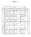
- FIG. 1 illustrates a schematic diagram showing a structure of a light emitting display device according to a first embodiment
- FIG. 2 illustrates a circuit diagram showing a pixel circuit and a conversion circuit included in a data driver
- FIG. 3 illustrates a circuit diagram schematically illustrating a pixel circuit according to an embodiment
- FIG. 4 illustrates a timing diagram for describing an operation of a circuit shown in FIG. 2 ;
- FIG. 5 illustrates a diagram showing operations of a pixel circuit shown in FIG. 3 ;
- FIG. 6 illustrates a timing diagram showing signals used when a pixel circuit shown in FIG. 5 operates
- FIG. 7 illustrates a circuit diagram of a comparative example where a driving transistor is directly connected to a data line
- FIG. 8 illustrates an example where writing of data at other pixel circuits connected with data lines on the same line and light emitting are performed in turn;
- FIG. 9 illustrates a circuit diagram of a light emitting display device according to a second embodiment
- FIG. 10 illustrates a timing diagram for describing an operation of a circuit shown in FIG. 9 ;
- FIG. 11 illustrates a circuit diagram of a light emitting display device according to a third embodiment
- FIG. 12 illustrates a timing diagram for describing an operation of a circuit shown in FIG. 11 ;
- FIG. 13 illustrates a circuit diagram of a light emitting display device according to a fourth embodiment
- FIG. 14 illustrates a timing diagram for describing an operation of a circuit shown in FIG. 13 .
- a pixel circuit driving a light emitting element and a display device using the same will be more fully described with reference to accompanying drawings.
- the pixel circuit driving a light emitting element and the display device using the same may be modified or changed variously, without departing from the scope thereof, and may not be limited to embodiments to be described later.
- the same portions or portions having the same function may be marked by the same reference numerals, and a duplicated description may be thus omitted.
- FIG. 1 is a schematic diagram showing a structure of a light emitting display device according to a first embodiment.
- a light emitting display device includes a display panel 1 , an emission driver 10 , a scan driver 20 , and a data driver 30 .
- the display panel 1 includes pixel circuits 100 arranged in a matrix of n rows and m columns.
- the pixel circuits 100 are controlled by the emission driver 10 , the scan driver 20 , and the data driver 30 .
- n is 1, 2, 3 . . .
- m is 1, 2, 3 . . . .
- the emission driver 10 is a driving circuit that controls a time at which a power supply voltage is supplied to the pixel circuits 100 .
- the emission driver 10 supplies a first emission control signal EMa(n) and a second emission control signal EMb(n) to emission control signals 11 and 12 that correspond to each of rows of pixel circuits 100 .
- the scan driver 20 is a driving circuit that selects a row in which data is to be written.
- the scan driver 20 supplies a gate control signal Scan (n) to a gate control line 21 / 22 corresponding to each row of pixel circuits 100 .
- each row may be selected in a non-sequential and exclusive manner according to a predetermined order.
- the data driver 30 is a driving circuit that determines a gray scale based on input image data and supplies a data voltage corresponding to the determined gray scale to the pixel circuit 100 .
- the data driver 30 supplies a data signal DTa(m) to a data signal line 31 corresponding to each of columns of pixel circuits 100 .
- the data signal DTa(m) may include a gray scale data voltage Vdata(m) of a pixel and an anode power ELVDD for supplying a current to a light emitting element, which are converted through a conversion circuit included in the data driver 30 .
- FIG. 2 is a circuit diagram of a pixel circuit 100 and a conversion circuit 40 included in a data driver 30 .
- FIG. 2 shows an example in which all transistors forming a pixel circuit are p-type.
- a connection between a gate control signal Scan(n) and each pixel circuit will be described with reference to FIG. 2 .
- a switch transistor M 3 of the pixel circuit 100 A and a switch transistor M 2 in the second row are controlled at the same time, e.g., using a same signal.
- a circuit operation will be more fully described later. If a circuit is configured as described above, a threshold voltage compensation operation of the pixel circuit 100 A and an initialization operation of the pixel circuit 100 B are simultaneously performed. Therefore, gray scale data is written such that efficiency is improved in a non-emission interval of a light emitting element.
- the conversion circuit 40 will be described with reference to FIG. 2 .
- the conversion circuit 40 receives the gray scale data voltage Vdata(m) and the anode voltage ELVDD, and is controlled by first and second gate control signals DCTL 1 and DCTL 2 .
- first and second gate control signals DCTL 1 and DCTL 2 For example, when transistors M 6 ( 1 ) and M 6 ( 2 ) are turned on by a first gate control signal DCTL 1 , the gray scale data voltage Vdata(m) is supplied to pixel circuits 100 A and 100 B.
- transistors M 7 ( 1 ) and M 7 ( 2 ) are turned on by a second gate control signal DCTL 2 , the anode voltage ELVDD is supplied to a pixel circuit.
- FIG. 3 is a circuit diagram schematically illustrating the pixel circuit 100 according to an embodiment.
- all transistors forming a pixel circuit are p-type.
- the pixel circuit 100 may include a driving transistor M 1 , switch transistors M 2 and M 3 , emission transistors M 4 and M 5 , a capacitor Cst, and a light emission element D 1 .
- the light emission element D 1 may be formed of a diode and a parasitic capacitance.
- the pixel circuit 100 is made up of five transistors M 1 to M 5 and a capacitor Cst.
- a connection between elements of the pixel circuit 100 will be described with reference to FIG. 3 .
- a cathode electrode of the light emitting element D 1 is connected to a cathode voltage ELVSS.
- the driving transistor M 1 controls the amount of current to be supplied to the light emitting element D 1 according to a voltage supplied to its gate electrode.
- the gate electrode of the light emitting element D 1 is connected to an initialization voltage Vinit through the switch transistor M 2 .
- the switch transistor M 3 is connected between the gate electrode of the driving transistor M 1 and one of source and drain electrodes thereof.
- the gate electrode of the driving transistor M 1 is connected to a first electrode of the capacitor Cst retaining gray scale data and a second electrode of the capacitor Cst is connected to the initialization voltage Vinit.
- the emission transistor M 4 is connected between one of the source and drain electrodes of the driving transistor M 1 and an anode electrode of the light emitting element D 1 .
- the other of the source and drain electrodes of the driving transistor M 1 is connected to a data line 31 through the emission transistor M 5 .
- FIG. 5 is a diagram showing operations of a pixel circuit shown in FIG. 3 .
- FIG. 6 is a timing diagram showing signals used when a pixel circuit shown in FIG. 5 operates.
- (A), (B), (C), and (D) indicate an initialization interval, a data line charging interval, a threshold voltage compensation interval, and a light emitting interval, respectively. Intervals shown in FIGS. 5 and 6 may be substantially the same.
- a timing diagram shown in FIG. 6 represents potentials of nodes, an M 1 source waveform corresponds to a potential of the source electrode of the M 1 transistor shown in FIG. 5 , and an M 1 gate waveform corresponds to a potential of a gate electrode of the M 1 transistor shown in FIG. 5 .
- the switch transistor M 2 When the switch transistor M 2 is turned on in response to a high-to-low transition of a gate control signal Scan(n ⁇ 1), the gate electrode of the driving transistor M 1 is connected to the initialization voltage Vinit. Thus, the pixel circuit 100 is reset. At this time, the first gate control signal DCTL 1 of the conversion circuit 40 goes to a low level, the second gate control signal DCTL 2 goes to a high level, and the gray scale data voltage Vdata(m) is supplied to a data line. When the gate control signal Scan(n ⁇ 1) has a low-to-high transition, the switch transistor M 2 is turned off. That is, initialization on the pixel circuit 100 is terminated.
- the switch transistor M 3 and the emission transistor M 5 of the pixel circuit 100 are turned on.
- the gray scale data voltage Vdata supplied to the data line is transferred to a gate electrode of the transistor M 1 through the transistor M 5 , the transistor M 1 , and the transistor M 3 .
- the switch transistor M 3 is diode-connected.
- a voltage lower by a threshold voltage of the transistor M 1 than the gray scale data voltage Vdata is supplied to the gate electrode of the transistor M 1 . This operation is referred to as a threshold voltage compensation operation.
- the threshold voltage compensation operation influence due to a variation in a threshold voltage of the driving transistor M 1 may be suppressed and a current flowing from a data line 31 to a light emitting element D 1 more be accurately controlled.
- the transistor M 3 of the pixel circuit 100 is turned off in response to a low-to-high transition of the gate control signal Scan(n). That is, the threshold voltage compensation operation is ended.
- an anode voltage ELVDD is supplied to the light emitting element D 1 through the transistor M 5 , the transistor M 1 , and the transistor M 4 . That is, the light emitting element D 1 emits light.
- FIG. 4 is a timing diagram for describing an operation of a circuit shown in FIG. 2 . An operation of pixel circuits will be described with reference to FIGS. 2 and 4 .
- a first frame period in which data is written to all pixel circuits of a display panel and light emission is performed is divided into a first field FD 1 and a second field FD 2 .
- the first field FD 1 is defined as a gray scale data writing interval (or, a non-light emitting interval)
- the second field FD 2 is defined as a light emitting interval.
- a gray scale data voltage Vdata(m) is supplied as a data signal DTa.
- the first gate control signal DCTL 1 of the conversion circuit has a high level
- the second gate control signal DCTL 2 has a low level.
- the transistors M 6 ( 1 ) and M 6 ( 2 ) are turned off, and the transistors M 7 ( 1 ) and M 7 ( 2 ) are turned on.
- an anode voltage ELVDD is supplied as the data signal DTa.
- a pixel circuit 100 A at a first column and a first row and a pixel circuit 100 B at the first column and a second row will be described with reference to FIG. 4 .
- initialization is performed by setting a gate control signal Scan( 1 ) to a low level and turning on a transistor M 2 of the pixel circuit 100 A.
- the pixel circuit 100 A may correspond to an initialization interval (A).
- the pixel circuit 100 A becomes off by setting the gate control signal Scan( 1 ) to a high level. That is, initialization is terminated.
- a data line 31 is charged by supplying a gray scale data voltage Vdata( 1 ) as a data signal DTa( 1 ).
- the pixel circuit 100 A may correspond to a data line charging interval (B).
- a gate control signal Scan( 2 ) and a first emission control signal EMa( 1 ) are simultaneously set to a low level, so a transistor M 3 of the pixel circuit 100 A is turned on. That is, a threshold voltage compensation operation is performed. Also, during the same interval, a switch transistor M 2 of the pixel circuit 100 B at the first column and the second row is turned on, and the pixel circuit 100 B is reset. At this time, the pixel circuit 100 A may correspond to a threshold voltage compensation interval (C), and the pixel circuit 100 B may correspond to the initialization interval (A).
- pixel circuits 100 A and 100 B (refer to FIG. 2 ) of the display panel 1 (refer to FIG. 1 ) sequentially perform an initialization operation, a data line charging operation, and a threshold voltage compensation operation. If a gray scale data signal is written to all the pixel circuits 100 A and 100 B, switching from the first field FD 1 to the second field FD 2 is made.
- a light emitting element D 1 emits a light when an anode voltage ELVDD is supplied to each pixel circuit 100 through data lines 31 and 32 .
- the pixel circuits 100 A and 100 B may correspond to a light emitting interval (D).
- gray scale data is written to each pixel circuit in the first field FD 1 , and a simultaneous driving operation for simultaneous light emitting is performed in the second field FD 2 .
- FIG. 7 is a circuit diagram schematically illustrating a comparative example where a driving transistor is directly connected to a data line.
- a pixel circuit shown in FIG. 7 includes four transistors and a capacitor. In this pixel circuit, a driving transistor of each pixel may be directly connected to a data line.
- a driving transistor M 1 a(n) is directly connected to a data line as shown in FIG. 7 , a crosstalk is generated due to a parasitic capacitance Cp(n) formed between a source/drain electrode and a gate electrode of the driving transistor M 1 a(n), thereby lowering the quality of display.
- FIG. 8 shows an example where writing of data at other pixel circuits connected with data lines DTa( 1 ) and DTa( 2 ) on the same line and light emitting are performed in turn. Alternating switching is performed between a gray scale data voltage VdataA/VdataB and an anode voltage ELVDD every one horizontal scan interval (1H).
- This example shows a gate potential GA(n) of a driving transistor M 1 a(n) of a pixel circuit PIXELa( 1 ) and a gate potential GB(n) of a driving transistor M 1 b(n) of a pixel circuit PIXELb( 1 ) in the event that the amplitude of the gray scale data voltage VdataA is larger than that of the gray scale data voltage VdataB.
- the gate potentials GA(n) and GB(n) are fluctuated due to influence of the parasitic capacitance CP(n). Influence on a gate electrode of a transistor M 1 a(n) connected increases in proportion to an increase in the amplitude of a data voltage.
- a potential variation of the gate electrode of the transistor M 1 a(n) causes a variation in brightness, thereby resulting in a crosstalk.
- the driving transistor M 1 is not influenced by a voltage variation of a data signal supplied to a data line, and the image quality is improved through suppression of a crosstalk.
- FIG. 9 is a circuit diagram schematically illustrating a light emitting display device according to a second embodiment.
- the second embodiment is different from a first embodiment in that two data lines 31 and 32 exist, an odd-numbered row of pixel circuits is connected to the data line 31 , and an oven-numbered row of pixel circuit is connected to the data line 32 .
- a conversion circuit is also configured to supply signals that are independent from a data signal to be supplied to the odd-numbered row of pixel circuits and from a data signal to be supplied to the even-numbered row of pixel circuits.
- FIG. 10 is a timing diagram for describing an operation of a circuit shown in FIG. 9 .
- a first frame period is divided into a first field FD 1 and a second field FD 2 .
- a first gate control signal DCTL 1 of the conversion circuit has a low level
- a second gate control signal DCTL 2 thereof has a high level.
- a gray scale data signal Vdata is supplied to data lines DTa and DTb.
- the first gate control signal DCTL 1 of the conversion circuit has a high level
- the second gate control signal DCTL 2 thereof has a low level.
- an anode voltage ELVDD is supplied to the data lines DTa and DTb.
- a pixel circuit 100 C at a first column and a second row and a pixel circuit 100 D at the first column and a third row will be described with reference to a timing diagram shown in FIG. 10 .
- the pixel circuit 100 C is reset by setting a gate control signal Scan( 1 ) to a low level.
- the pixel circuit 100 C may correspond to an initialization interval (A).
- the pixel circuit 100 D is reset by setting a gate control signal Scan( 2 ) to a low level. During the same interval, also, a gray scale data voltage Vdata( 2 ) is supplied to a data line DTb to charge a data line 34 .
- the pixel circuit 100 C may correspond to a data line charging interval (B), and the pixel circuit 100 D may correspond to the initialization interval (A).
- a threshold voltage compensation operation of the pixel circuit 100 C is performed by setting a gate control signal Scan( 3 ) and a first emission control signal EMa( 2 ) to a low level.
- a gray scale data voltage Vdata( 3 ) is provided to a data line DTa to charge a data line 33 .
- the pixel circuit 100 C may correspond to a threshold voltage compensation interval (C)
- the pixel circuit 100 D may correspond to the data line charging interval (B).
- the threshold voltage compensation operation of the pixel circuit 100 C is ended by setting the gate control signal Scan( 3 ) and the first emission control signal EMa( 2 ) to a high level.
- the threshold voltage compensation operation of the pixel circuit 100 D is performed by setting the gate control signal Scan( 4 ) and the first emission control signal EMa( 3 ) to a low level.
- the pixel circuit 100 D may correspond to the threshold voltage compensation interval (C).
- the threshold voltage compensation operation of the pixel circuit 100 D is ended by setting the gate control signal Scan( 4 ) and the first emission control signal EMa( 3 ) to a high level.
- an initialization operation, a data line charging operation, and a threshold voltage compensation operation about pixel circuits in a panel are performed in a line-sequential manner. If gray scale data is written to all pixel circuits of the panel, switching from the first field FD 1 to the second field FD 2 is made, and light emitting elements emit light when the anode voltage ELVDD is supplied to pixels through the data lines 33 and 34 . At this time, each of the pixel circuits 100 C and 100 D may correspond to a light emitting interval. In exemplary embodiments, gray scale data is written to each pixel circuit in the first field FD 1 , and a simultaneous driving operation for simultaneous light emitting is performed in the second field FD 2 .
- gray scaly data corresponding to an even-numbered row and gray scaly data corresponding to an odd-numbered row are supplied to overlap within an interval.
- a threshold voltage compensation operation about an odd-numbered row of pixel circuits is performed while charging data lines corresponding to an even-numbered row. Since a charging interval of the first embodiment corresponds to a threshold voltage compensation operation, it is possible to implement double a threshold voltage compensation interval with the same duty ratio.
- the output intervals of two data signals always overlap.
- embodiments are not limited thereto. For example, output intervals of two data signals may partially overlap.
- FIG. 11 is a circuit diagram schematically illustrating a light emitting display device according to a third embodiment.
- a connection between a switch transistor M 2 and an emission transistor M 4 is different from that according to a second embodiment.
- FIG. 12 is a timing diagram for describing an operation of a circuit shown in FIG. 11 .
- each of 1 horizontal scan intervals 1 H is broken down into a first field FD 1 and a second field FD 2 .
- a first gate control signal DCTL 1 of a conversion circuit is set to a low level
- a second gate control signal DCTL 2 thereof is set to a high level.
- a gray scale data voltage Vdata is supplied to a data line DTa
- ELVDD is supplied to a data line DTb.
- gray scale data is written to a first row of pixel circuits, and other odd-numbered rows of pixel circuits are set to a non-emission interval.
- An odd-numbered row may correspond to a first field FD 1 .
- even-numbered rows of pixel circuits all are set to an emission interval and may correspond to a second field FD 2 .
- the first gate control signal DCTL 1 of the conversion circuit is set to a high level, and the second gate control signal DCTL 2 thereof is set to a low level.
- the anode voltage ELVDD is supplied to the data line DTa, and the gray scale data voltage Vdata is supplied to the data line DTb.
- an odd-numbered row may correspond to the first field FD 2
- an even-numbered row may correspond to the first field FD 1 .
- gray scale data is written to an odd-numbered row of pixel circuits (first field FD 1 ), and an even-numbered row of pixel circuits emit light (second field FD 2 ).
- gray scale data is written to an even-numbered row of pixel circuits (first field FD 1 ), and an odd-numbered row of pixel circuits emit light (second field FD 2 ).
- a gate control signal Scan( 1 ) is set to a low level during the second field FD 2 immediately before gray scale data is written, and the pixel circuit 100 E is reset. At this time, the pixel circuit 100 E may correspond to an initialization interval. As a first emission control signal EMa( 1 ) and a second emission control signal EMb are set to a high level, the pixel circuit 100 E does not emit light, and other odd-numbered rows of pixel circuits emit light.
- the pixel circuit 100 E goes to the first field FD 1 , a gray scale data voltage Vdata( 1 ) is supplied to a data line DTa, and a data line 35 is charged. At this time, the pixel circuit 100 E may correspond to a data line charging interval.
- a threshold voltage compensation operation of the pixel circuit 100 E is performed by setting a gate control signal Scan( 2 ) and a first emission control signal EMa( 1 ) to a low level (the pixel circuit 100 E corresponding to the first field FD 1 ).
- a pixel circuit 100 F may be reset (the pixel circuit 100 F corresponding to the second field FD 2 ).
- the pixel circuit 100 F may correspond to an initialization interval (A).
- the threshold voltage compensation operation of the pixel circuit 100 E is ended by setting the gate control signal Scan( 2 ) to a high level.
- an anode voltage ELVDD is supplied to the pixel circuit 100 E through a data line 35 by setting a second emission control signal EMb( 1 ) to a low level, with a first emission control signal EMa( 1 ) set to a low level. That is, a light emitting element emits light.
- charging of a data line 36 and a threshold voltage compensation operation are performed in the pixel circuit 100 F (the pixel circuit 100 F corresponding to the first field FD 1 ).
- the pixel circuit 100 E may correspond to a light emitting interval (D), and the pixel circuit 100 F may correspond to a data line charging interval (B) and a threshold voltage compensation interval (C).
- Such operations are the same as those of the pixel circuit 100 E, and a description thereof is thus omitted.
- a light emitting element of the pixel circuit 100 E does not emit light (FD 1 ), and a light emitting element of the pixel circuit 100 F emits light (FD 2 ).
- the pixel circuit 100 F may correspond to the light emitting interval (D).
- the first field FD 1 and the second field FD 2 are repeated, and light emitting and non-light emitting are switched within one frame.
- gray scale data is written to an odd-numbered row of pixel circuits and an even-numbered row of pixel circuits emit light.
- gray scale data is written to an even-numbered row of pixel circuits and an odd-numbered row of pixel circuits emit light. That is, a progressive driving method where pixel circuits in either an even-numbered row or an odd-numbered row emit light is used.
- FIG. 13 is a circuit diagram schematically illustrating a light emitting display device according to a fourth embodiment.
- a fourth embodiment is different from a third embodiment in that an emission transistor M 4 is connected every odd-numbered row and every even-numbered TOW.
- FIG. 14 is a timing diagram for describing an operation of a circuit shown in FIG. 13 .
- a frame period is divided into a first field FD 1 and a second field FD 2 .
- a first gate control signal DCTL 1 of a conversion circuit is set to a low level and a second gate control signal DCTL 2 is set to a high level.
- a gray scale data voltage is supplied to a data line DTa and an anode voltage ELVDD is supplied to a data line DTb.
- an odd-numbered row of pixel circuits may correspond to a first field FD 1
- an even-numbered row of pixel circuits may correspond to a second field FD 2 .
- the first gate control signal DCTL 1 of the conversion circuit is set to a high level and the second gate control signal DCTL 2 thereof is set to a low level.
- the anode voltage ELVDD is supplied to the data line DTa and the gray scale data voltage Vdata is supplied to the data line DTb.
- an odd-numbered row may correspond to the first field FD 2
- an even-numbered row may correspond to the first field FD 1 .
- the pixel circuit 100 G is reset by setting a gate control signal Scan( 1 ) to a low level.
- the pixel circuit 100 A may correspond to an initialization interval (A).
- a gray scale data voltage Vdata( 1 ) is supplied to a data line DTa to charge a data line 301 .
- the pixel circuit 100 G may correspond to a data line charging interval (B).
- a threshold voltage compensation operation of the pixel circuit 100 G is performed by setting a gate control signal Scan( 3 ) and a first emission control signal EMa( 1 ) to a low level.
- the pixel circuit 100 H is reset.
- the pixel circuit 100 H may correspond to an initialization interval (A).
- the threshold voltage compensation operation of the pixel circuit 100 G and the initialization operation of the pixel circuit 100 H are ended by setting the gate control signal Scan( 3 ) and the first emission control signal EMa( 1 ) to a high level.
- a data line 301 is charged by supplying the gray scale data voltage Vdata( 3 ) as a data signal DTa.
- the pixel circuit 100 H may correspond to a data line charge interval (B).
- the threshold voltage compensation operation of the pixel circuit 100 H is performed by setting the gate control signal Scan( 5 ) and the first emission control signal EMa( 3 ) to a low level.
- the pixel circuit 100 H may correspond to the threshold voltage compensation interval (C).
- an initialization operation, a data line charging operation, and a threshold voltage compensation operation about an odd-numbered row of pixel circuits in a panel are performed in a line-sequential manner. If gray scale data is written to all pixel circuits in an odd-numbered row of the panel, a field is switched, and light emitting elements emit light upon supplying of an anode voltage ELVDD to an odd-numbered row of pixels through the data line 301 (pixel circuits 100 G and 100 H corresponding to a light emitting interval (D)). In exemplary embodiments, during one field, gray scale data is written to an odd-numbered row of pixel circuits and an even-numbered row of pixel circuits emit light.
- gray scale data is written to an even-numbered row of pixel circuits and an odd-numbered row of pixel circuits emit light. That is, a progressive driving method where pixel circuits in either an even-numbered row or an odd-numbered row emit light is used.
- circuits according to the first to fourth embodiments may be formed of N-channel transistors or both N-channel transistors and P-channel transistors (CMOS type).
- first field FD 1 and a second field FD 2 are controlled every odd-numbered row and every even-numbered row.
- the embodiments are not limited thereto.
- a combination of rows controlled in the first and second fields FD 1 and FD 2 may be randomly selected.
- 3D images may be provided in an active shutter manner by outputting an image for right eye to an odd-numbered row and an image for left eye to an even-numbered row.
- the number of elements per pixel is reduced, and a pixel circuit with a conventional threshold voltage compensation capacity is provided.
- a panel becomes more precise, and a yield is improved.
- a data line is not directly connected to a driving transistor of controlling the amount of current to be supplied to a light emitting element, a voltage of a data signal transferred via the data line does not vary. Accordingly, a gate potential of the driving transistor may be maintained.
- image quality is improved by reducing or eliminating errors such as a crosstalk.
Applications Claiming Priority (2)
| Application Number | Priority Date | Filing Date | Title |
|---|---|---|---|
| JP2013097859A JP2014219516A (ja) | 2013-05-07 | 2013-05-07 | 画素回路及びその駆動方法 |
| JP2013-097859 | 2013-05-07 |
Publications (2)
| Publication Number | Publication Date |
|---|---|
| US20140333214A1 US20140333214A1 (en) | 2014-11-13 |
| US9412295B2 true US9412295B2 (en) | 2016-08-09 |
Family
ID=51864302
Family Applications (1)
| Application Number | Title | Priority Date | Filing Date |
|---|---|---|---|
| US14/269,439 Active 2034-09-16 US9412295B2 (en) | 2013-05-07 | 2014-05-05 | Pixel circuit and driving method thereof |
Country Status (3)
| Country | Link |
|---|---|
| US (1) | US9412295B2 (ja) |
| JP (1) | JP2014219516A (ja) |
| KR (1) | KR102137521B1 (ja) |
Cited By (1)
| Publication number | Priority date | Publication date | Assignee | Title |
|---|---|---|---|---|
| US11568811B2 (en) * | 2020-06-22 | 2023-01-31 | Lg Display Co., Ltd. | Electroluminescence display apparatus |
Families Citing this family (9)
| Publication number | Priority date | Publication date | Assignee | Title |
|---|---|---|---|---|
| KR102068263B1 (ko) * | 2013-07-10 | 2020-01-21 | 삼성디스플레이 주식회사 | 유기 발광 표시 장치 및 그 구동 방법 |
| CN104123912B (zh) * | 2014-07-03 | 2016-10-19 | 京东方科技集团股份有限公司 | 像素电路及其驱动方法、显示装置 |
| CN104409043B (zh) | 2014-12-05 | 2016-08-24 | 京东方科技集团股份有限公司 | 像素驱动电路和像素驱动方法、显示装置 |
| CN107256694B (zh) * | 2017-07-31 | 2019-11-05 | 武汉华星光电半导体显示技术有限公司 | 显示装置、像素驱动方法及像素驱动电路 |
| KR20210077087A (ko) * | 2019-12-16 | 2021-06-25 | 삼성디스플레이 주식회사 | 발광 구동부 및 이를 포함하는 표시장치 |
| CN111564136B (zh) * | 2020-07-16 | 2020-10-23 | 武汉华星光电半导体显示技术有限公司 | 像素电路及驱动方法、显示面板 |
| CN114694580B (zh) * | 2022-03-31 | 2023-07-04 | 武汉天马微电子有限公司 | 一种显示面板及其驱动方法、显示装置 |
| CN114974084B (zh) * | 2022-05-12 | 2023-09-26 | 惠科股份有限公司 | 显示单元的驱动电路、方法以及显示装置 |
| CN115331618B (zh) * | 2022-10-12 | 2023-01-06 | 惠科股份有限公司 | 驱动电路、显示面板和显示装置 |
Citations (9)
| Publication number | Priority date | Publication date | Assignee | Title |
|---|---|---|---|---|
| JP2005128521A (ja) | 2003-09-30 | 2005-05-19 | Sanyo Electric Co Ltd | 有機el画素回路 |
| JP2008151963A (ja) | 2006-12-15 | 2008-07-03 | Semiconductor Energy Lab Co Ltd | 半導体装置及び半導体装置の駆動方法 |
| JP2008225506A (ja) | 2002-04-26 | 2008-09-25 | Toshiba Matsushita Display Technology Co Ltd | El表示装置 |
| JP2009204664A (ja) | 2008-02-26 | 2009-09-10 | Sony Corp | 表示装置、表示装置の駆動方法および電子機器 |
| JP2009265328A (ja) | 2008-04-24 | 2009-11-12 | Toshiba Mobile Display Co Ltd | El表示装置。 |
| JP2011199214A (ja) | 2010-03-24 | 2011-10-06 | Hitachi Kokusai Electric Inc | 熱処理装置、半導体装置の製造方法、及び、基板の製造方法 |
| US20120001896A1 (en) * | 2010-06-30 | 2012-01-05 | Samsung Mobile Display Co., Ltd. | Pixel and organic light emitting display device using the same |
| JP2013061452A (ja) | 2011-09-13 | 2013-04-04 | Samsung Display Co Ltd | 画素回路、および表示装置 |
| US20130293600A1 (en) * | 2012-05-02 | 2013-11-07 | Lg Display Co., Ltd. | Organic light-emitting diode display, circuit and method for driving thereof |
Family Cites Families (1)
| Publication number | Priority date | Publication date | Assignee | Title |
|---|---|---|---|---|
| JP2006106568A (ja) * | 2004-10-08 | 2006-04-20 | Sharp Corp | 表示装置 |
-
2013
- 2013-05-07 JP JP2013097859A patent/JP2014219516A/ja active Pending
-
2014
- 2014-03-03 KR KR1020140025108A patent/KR102137521B1/ko active IP Right Grant
- 2014-05-05 US US14/269,439 patent/US9412295B2/en active Active
Patent Citations (9)
| Publication number | Priority date | Publication date | Assignee | Title |
|---|---|---|---|---|
| JP2008225506A (ja) | 2002-04-26 | 2008-09-25 | Toshiba Matsushita Display Technology Co Ltd | El表示装置 |
| JP2005128521A (ja) | 2003-09-30 | 2005-05-19 | Sanyo Electric Co Ltd | 有機el画素回路 |
| JP2008151963A (ja) | 2006-12-15 | 2008-07-03 | Semiconductor Energy Lab Co Ltd | 半導体装置及び半導体装置の駆動方法 |
| JP2009204664A (ja) | 2008-02-26 | 2009-09-10 | Sony Corp | 表示装置、表示装置の駆動方法および電子機器 |
| JP2009265328A (ja) | 2008-04-24 | 2009-11-12 | Toshiba Mobile Display Co Ltd | El表示装置。 |
| JP2011199214A (ja) | 2010-03-24 | 2011-10-06 | Hitachi Kokusai Electric Inc | 熱処理装置、半導体装置の製造方法、及び、基板の製造方法 |
| US20120001896A1 (en) * | 2010-06-30 | 2012-01-05 | Samsung Mobile Display Co., Ltd. | Pixel and organic light emitting display device using the same |
| JP2013061452A (ja) | 2011-09-13 | 2013-04-04 | Samsung Display Co Ltd | 画素回路、および表示装置 |
| US20130293600A1 (en) * | 2012-05-02 | 2013-11-07 | Lg Display Co., Ltd. | Organic light-emitting diode display, circuit and method for driving thereof |
Cited By (1)
| Publication number | Priority date | Publication date | Assignee | Title |
|---|---|---|---|---|
| US11568811B2 (en) * | 2020-06-22 | 2023-01-31 | Lg Display Co., Ltd. | Electroluminescence display apparatus |
Also Published As
| Publication number | Publication date |
|---|---|
| JP2014219516A (ja) | 2014-11-20 |
| US20140333214A1 (en) | 2014-11-13 |
| KR102137521B1 (ko) | 2020-07-27 |
| KR20140133415A (ko) | 2014-11-19 |
Similar Documents
| Publication | Publication Date | Title |
|---|---|---|
| US9412295B2 (en) | Pixel circuit and driving method thereof | |
| KR102570832B1 (ko) | Oled 표시 장치 및 그의 구동 방법 | |
| US9697768B2 (en) | Organic light-emitting display apparatus | |
| US9084331B2 (en) | Active matrix organic light emitting diode circuit and operating method of the same | |
| KR101082234B1 (ko) | 유기전계발광 표시장치 및 그의 구동방법 | |
| US9647047B2 (en) | Organic light emitting display for initializing pixels | |
| KR101182238B1 (ko) | 유기 발광 표시장치 및 그의 구동방법 | |
| US9105236B2 (en) | Light emitting display device | |
| KR101162864B1 (ko) | 화소 및 이를 이용한 유기 전계발광 표시장치 | |
| US9633598B2 (en) | Pixel circuit and driving method thereof | |
| US9262962B2 (en) | Pixel and organic light emitting display device using the same | |
| US8610701B2 (en) | Organic light emitting display device with pixel configured to be driven during frame period and driving method thereof | |
| KR101210029B1 (ko) | 유기전계발광 표시장치 | |
| WO2010134263A1 (ja) | 表示装置及びその駆動方法 | |
| KR102206602B1 (ko) | 화소 및 이를 이용한 유기전계발광 표시장치 | |
| US9318052B2 (en) | Compensating organic light emitting diode display device and method for driving the same using two adjacent gate lines per pixel | |
| KR101681210B1 (ko) | 유기 전계발광 표시장치 | |
| KR20170122432A (ko) | Oled 표시 장치 및 그의 구동 방법 | |
| JP5414808B2 (ja) | 表示装置およびその駆動方法 | |
| KR101970544B1 (ko) | 유기 발광 다이오드 표시장치와 그 구동방법 | |
| KR20120053688A (ko) | 유기 발광 다이오드 표시장치와 그 구동방법 | |
| KR101689323B1 (ko) | 유기 전계발광 표시장치 및 그의 구동방법 | |
| WO2013164965A1 (ja) | 電気光学装置およびその駆動方法 | |
| KR20140068559A (ko) | 유기전계발광표시장치와 이의 구동방법 | |
| WO2012032562A1 (ja) | 表示装置およびその駆動方法 |
Legal Events
| Date | Code | Title | Description |
|---|---|---|---|
| AS | Assignment |
Owner name: SAMSUNG DISPLAY CO., LTD., KOREA, REPUBLIC OF Free format text: ASSIGNMENT OF ASSIGNORS INTEREST;ASSIGNORS:OKUNO, TAKESHI;KUMETA, MASAYUKI;KANDA, EIJI;AND OTHERS;REEL/FRAME:032820/0067 Effective date: 20140423 |
|
| FEPP | Fee payment procedure |
Free format text: PAYOR NUMBER ASSIGNED (ORIGINAL EVENT CODE: ASPN); ENTITY STATUS OF PATENT OWNER: LARGE ENTITY |
|
| STCF | Information on status: patent grant |
Free format text: PATENTED CASE |
|
| MAFP | Maintenance fee payment |
Free format text: PAYMENT OF MAINTENANCE FEE, 4TH YEAR, LARGE ENTITY (ORIGINAL EVENT CODE: M1551); ENTITY STATUS OF PATENT OWNER: LARGE ENTITY Year of fee payment: 4 |
|
| MAFP | Maintenance fee payment |
Free format text: PAYMENT OF MAINTENANCE FEE, 8TH YEAR, LARGE ENTITY (ORIGINAL EVENT CODE: M1552); ENTITY STATUS OF PATENT OWNER: LARGE ENTITY Year of fee payment: 8 |