US9368699B2 - Semiconductor component containing a highly refractive polymer material - Google Patents
Semiconductor component containing a highly refractive polymer material Download PDFInfo
- Publication number
- US9368699B2 US9368699B2 US13/703,180 US201113703180A US9368699B2 US 9368699 B2 US9368699 B2 US 9368699B2 US 201113703180 A US201113703180 A US 201113703180A US 9368699 B2 US9368699 B2 US 9368699B2
- Authority
- US
- United States
- Prior art keywords
- optical element
- semiconductor chip
- semiconductor
- semiconductor component
- radiation
- Prior art date
- Legal status (The legal status is an assumption and is not a legal conclusion. Google has not performed a legal analysis and makes no representation as to the accuracy of the status listed.)
- Active, expires
Links
Images


Classifications
-
- H—ELECTRICITY
- H10—SEMICONDUCTOR DEVICES; ELECTRIC SOLID-STATE DEVICES NOT OTHERWISE PROVIDED FOR
- H10H—INORGANIC LIGHT-EMITTING SEMICONDUCTOR DEVICES HAVING POTENTIAL BARRIERS
- H10H20/00—Individual inorganic light-emitting semiconductor devices having potential barriers, e.g. light-emitting diodes [LED]
- H10H20/80—Constructional details
- H10H20/85—Packages
- H10H20/852—Encapsulations
-
- H01L33/507—
-
- B—PERFORMING OPERATIONS; TRANSPORTING
- B29—WORKING OF PLASTICS; WORKING OF SUBSTANCES IN A PLASTIC STATE IN GENERAL
- B29D—PRODUCING PARTICULAR ARTICLES FROM PLASTICS OR FROM SUBSTANCES IN A PLASTIC STATE
- B29D11/00—Producing optical elements, e.g. lenses or prisms
- B29D11/00009—Production of simple or compound lenses
- B29D11/00432—Auxiliary operations, e.g. machines for filling the moulds
- B29D11/00442—Curing the lens material
-
- C—CHEMISTRY; METALLURGY
- C08—ORGANIC MACROMOLECULAR COMPOUNDS; THEIR PREPARATION OR CHEMICAL WORKING-UP; COMPOSITIONS BASED THEREON
- C08L—COMPOSITIONS OF MACROMOLECULAR COMPOUNDS
- C08L63/00—Compositions of epoxy resins; Compositions of derivatives of epoxy resins
-
- C—CHEMISTRY; METALLURGY
- C08—ORGANIC MACROMOLECULAR COMPOUNDS; THEIR PREPARATION OR CHEMICAL WORKING-UP; COMPOSITIONS BASED THEREON
- C08L—COMPOSITIONS OF MACROMOLECULAR COMPOUNDS
- C08L75/00—Compositions of polyureas or polyurethanes; Compositions of derivatives of such polymers
-
- C—CHEMISTRY; METALLURGY
- C08—ORGANIC MACROMOLECULAR COMPOUNDS; THEIR PREPARATION OR CHEMICAL WORKING-UP; COMPOSITIONS BASED THEREON
- C08L—COMPOSITIONS OF MACROMOLECULAR COMPOUNDS
- C08L83/00—Compositions of macromolecular compounds obtained by reactions forming in the main chain of the macromolecule a linkage containing silicon with or without sulfur, nitrogen, oxygen or carbon only; Compositions of derivatives of such polymers
- C08L83/04—Polysiloxanes
-
- G—PHYSICS
- G02—OPTICS
- G02B—OPTICAL ELEMENTS, SYSTEMS OR APPARATUS
- G02B1/00—Optical elements characterised by the material of which they are made; Optical coatings for optical elements
- G02B1/04—Optical elements characterised by the material of which they are made; Optical coatings for optical elements made of organic materials, e.g. plastics
-
- G—PHYSICS
- G02—OPTICS
- G02B—OPTICAL ELEMENTS, SYSTEMS OR APPARATUS
- G02B27/00—Optical systems or apparatus not provided for by any of the groups G02B1/00 - G02B26/00, G02B30/00
- G02B27/09—Beam shaping, e.g. changing the cross-sectional area, not otherwise provided for
- G02B27/0938—Using specific optical elements
- G02B27/095—Refractive optical elements
-
- H01L33/483—
-
- H01L33/486—
-
- H01L33/501—
-
- H01L33/52—
-
- H01L33/54—
-
- H01L33/56—
-
- H—ELECTRICITY
- H10—SEMICONDUCTOR DEVICES; ELECTRIC SOLID-STATE DEVICES NOT OTHERWISE PROVIDED FOR
- H10H—INORGANIC LIGHT-EMITTING SEMICONDUCTOR DEVICES HAVING POTENTIAL BARRIERS
- H10H20/00—Individual inorganic light-emitting semiconductor devices having potential barriers, e.g. light-emitting diodes [LED]
- H10H20/01—Manufacture or treatment
- H10H20/036—Manufacture or treatment of packages
- H10H20/0362—Manufacture or treatment of packages of encapsulations
-
- H—ELECTRICITY
- H10—SEMICONDUCTOR DEVICES; ELECTRIC SOLID-STATE DEVICES NOT OTHERWISE PROVIDED FOR
- H10H—INORGANIC LIGHT-EMITTING SEMICONDUCTOR DEVICES HAVING POTENTIAL BARRIERS
- H10H20/00—Individual inorganic light-emitting semiconductor devices having potential barriers, e.g. light-emitting diodes [LED]
- H10H20/80—Constructional details
- H10H20/85—Packages
- H10H20/8506—Containers
-
- H—ELECTRICITY
- H10—SEMICONDUCTOR DEVICES; ELECTRIC SOLID-STATE DEVICES NOT OTHERWISE PROVIDED FOR
- H10H—INORGANIC LIGHT-EMITTING SEMICONDUCTOR DEVICES HAVING POTENTIAL BARRIERS
- H10H20/00—Individual inorganic light-emitting semiconductor devices having potential barriers, e.g. light-emitting diodes [LED]
- H10H20/80—Constructional details
- H10H20/85—Packages
- H10H20/851—Wavelength conversion means
- H10H20/8511—Wavelength conversion means characterised by their material, e.g. binder
-
- H—ELECTRICITY
- H10—SEMICONDUCTOR DEVICES; ELECTRIC SOLID-STATE DEVICES NOT OTHERWISE PROVIDED FOR
- H10H—INORGANIC LIGHT-EMITTING SEMICONDUCTOR DEVICES HAVING POTENTIAL BARRIERS
- H10H20/00—Individual inorganic light-emitting semiconductor devices having potential barriers, e.g. light-emitting diodes [LED]
- H10H20/80—Constructional details
- H10H20/85—Packages
- H10H20/851—Wavelength conversion means
- H10H20/8515—Wavelength conversion means not being in contact with the bodies
-
- H—ELECTRICITY
- H10—SEMICONDUCTOR DEVICES; ELECTRIC SOLID-STATE DEVICES NOT OTHERWISE PROVIDED FOR
- H10H—INORGANIC LIGHT-EMITTING SEMICONDUCTOR DEVICES HAVING POTENTIAL BARRIERS
- H10H20/00—Individual inorganic light-emitting semiconductor devices having potential barriers, e.g. light-emitting diodes [LED]
- H10H20/80—Constructional details
- H10H20/85—Packages
- H10H20/852—Encapsulations
- H10H20/853—Encapsulations characterised by their shape
-
- H—ELECTRICITY
- H10—SEMICONDUCTOR DEVICES; ELECTRIC SOLID-STATE DEVICES NOT OTHERWISE PROVIDED FOR
- H10H—INORGANIC LIGHT-EMITTING SEMICONDUCTOR DEVICES HAVING POTENTIAL BARRIERS
- H10H20/00—Individual inorganic light-emitting semiconductor devices having potential barriers, e.g. light-emitting diodes [LED]
- H10H20/80—Constructional details
- H10H20/85—Packages
- H10H20/852—Encapsulations
- H10H20/854—Encapsulations characterised by their material, e.g. epoxy or silicone resins
-
- H—ELECTRICITY
- H10—SEMICONDUCTOR DEVICES; ELECTRIC SOLID-STATE DEVICES NOT OTHERWISE PROVIDED FOR
- H10H—INORGANIC LIGHT-EMITTING SEMICONDUCTOR DEVICES HAVING POTENTIAL BARRIERS
- H10H20/00—Individual inorganic light-emitting semiconductor devices having potential barriers, e.g. light-emitting diodes [LED]
- H10H20/80—Constructional details
- H10H20/85—Packages
- H10H20/855—Optical field-shaping means, e.g. lenses
-
- H01L2224/32245—
-
- H01L2224/48091—
-
- H01L2224/48247—
-
- H01L2224/73265—
-
- H01L2224/8592—
-
- H01L2924/00—
-
- H01L2924/00014—
-
- H01L2933/005—
-
- H01L2933/0058—
-
- H01L33/50—
-
- H01L33/58—
-
- H—ELECTRICITY
- H10—SEMICONDUCTOR DEVICES; ELECTRIC SOLID-STATE DEVICES NOT OTHERWISE PROVIDED FOR
- H10H—INORGANIC LIGHT-EMITTING SEMICONDUCTOR DEVICES HAVING POTENTIAL BARRIERS
- H10H20/00—Individual inorganic light-emitting semiconductor devices having potential barriers, e.g. light-emitting diodes [LED]
- H10H20/01—Manufacture or treatment
- H10H20/036—Manufacture or treatment of packages
- H10H20/0363—Manufacture or treatment of packages of optical field-shaping means
-
- H—ELECTRICITY
- H10—SEMICONDUCTOR DEVICES; ELECTRIC SOLID-STATE DEVICES NOT OTHERWISE PROVIDED FOR
- H10H—INORGANIC LIGHT-EMITTING SEMICONDUCTOR DEVICES HAVING POTENTIAL BARRIERS
- H10H20/00—Individual inorganic light-emitting semiconductor devices having potential barriers, e.g. light-emitting diodes [LED]
- H10H20/80—Constructional details
- H10H20/85—Packages
- H10H20/857—Interconnections, e.g. lead-frames, bond wires or solder balls
-
- H—ELECTRICITY
- H10—SEMICONDUCTOR DEVICES; ELECTRIC SOLID-STATE DEVICES NOT OTHERWISE PROVIDED FOR
- H10W—GENERIC PACKAGES, INTERCONNECTIONS, CONNECTORS OR OTHER CONSTRUCTIONAL DETAILS OF DEVICES COVERED BY CLASS H10
- H10W72/00—Interconnections or connectors in packages
- H10W72/01—Manufacture or treatment
- H10W72/015—Manufacture or treatment of bond wires
- H10W72/01515—Forming coatings
-
- H—ELECTRICITY
- H10—SEMICONDUCTOR DEVICES; ELECTRIC SOLID-STATE DEVICES NOT OTHERWISE PROVIDED FOR
- H10W—GENERIC PACKAGES, INTERCONNECTIONS, CONNECTORS OR OTHER CONSTRUCTIONAL DETAILS OF DEVICES COVERED BY CLASS H10
- H10W72/00—Interconnections or connectors in packages
- H10W72/071—Connecting or disconnecting
- H10W72/075—Connecting or disconnecting of bond wires
-
- H—ELECTRICITY
- H10—SEMICONDUCTOR DEVICES; ELECTRIC SOLID-STATE DEVICES NOT OTHERWISE PROVIDED FOR
- H10W—GENERIC PACKAGES, INTERCONNECTIONS, CONNECTORS OR OTHER CONSTRUCTIONAL DETAILS OF DEVICES COVERED BY CLASS H10
- H10W72/00—Interconnections or connectors in packages
- H10W72/851—Dispositions of multiple connectors or interconnections
- H10W72/874—On different surfaces
- H10W72/884—Die-attach connectors and bond wires
-
- H—ELECTRICITY
- H10—SEMICONDUCTOR DEVICES; ELECTRIC SOLID-STATE DEVICES NOT OTHERWISE PROVIDED FOR
- H10W—GENERIC PACKAGES, INTERCONNECTIONS, CONNECTORS OR OTHER CONSTRUCTIONAL DETAILS OF DEVICES COVERED BY CLASS H10
- H10W90/00—Package configurations
- H10W90/701—Package configurations characterised by the relative positions of pads or connectors relative to package parts
- H10W90/731—Package configurations characterised by the relative positions of pads or connectors relative to package parts of die-attach connectors
- H10W90/736—Package configurations characterised by the relative positions of pads or connectors relative to package parts of die-attach connectors between a chip and a stacked lead frame, conducting package substrate or heat sink
-
- H—ELECTRICITY
- H10—SEMICONDUCTOR DEVICES; ELECTRIC SOLID-STATE DEVICES NOT OTHERWISE PROVIDED FOR
- H10W—GENERIC PACKAGES, INTERCONNECTIONS, CONNECTORS OR OTHER CONSTRUCTIONAL DETAILS OF DEVICES COVERED BY CLASS H10
- H10W90/00—Package configurations
- H10W90/701—Package configurations characterised by the relative positions of pads or connectors relative to package parts
- H10W90/751—Package configurations characterised by the relative positions of pads or connectors relative to package parts of bond wires
- H10W90/756—Package configurations characterised by the relative positions of pads or connectors relative to package parts of bond wires between a chip and a stacked lead frame, conducting package substrate or heat sink
Definitions
- This disclosure relates to a semiconductor component and to a method for producing a semiconductor component.
- a semiconductor component including an optoelectronic semiconductor chip and an optical element arranged on a radiation passage area of the semiconductor chip, wherein the optical element is based on a highly refractive polymer material.
- a method of producing a semiconductor component including providing an optoelectronic semiconductor chip, applying a molding compound for an optical element, wherein the molding compound is based on a highly refractive polymer material, procuring the molding compound at a temperature of at most 50° C. and curing the molding compound.
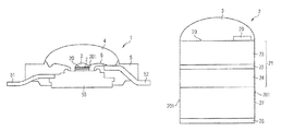
- FIG. 1 shows a first example of a semiconductor component in a schematic sectional view.
- FIG. 2 shows an enlarged illustration of a semiconductor chip and of an optical element in accordance with the first example illustrated in FIG. 1 .
- FIGS. 4A to 4E show illustrations of five examples of an optical element in each case in a sectional view.
- Our semiconductor component may comprise an optoelectronic semiconductor chip and an optical element arranged on a radiation passage area of the semiconductor chip.
- the optical element is based on a highly refractive polymer material.
- based on a highly refractive polymer material means that the highly refractive polymer material forms the basic material for the optical element. Further material can be admixed with the highly refractive polymer material as basic material, for example, luminescence conversion material to convert radiation generated in the semiconductor chip and/or diffuser material.
- the optical element contains highly refractive polymer material with a proportion by weight of at least 80%.
- a refractive index of the optical element in particular the polymer material of the optical element, is at least 1.52, particularly preferably at least 1.54. Furthermore, the refractive index of the optical element is expediently less than a refractive index of the semiconductor material of the semiconductor component facing the optical element.
- the optical element contains a silicone, an epoxide or a hybrid material.
- diphenylsiloxane is distinguished by a comparatively high refractive index of 1.54.
- the optical element adjoins the semiconductor chip, preferably directly.
- the optical element is molded onto the semiconductor chip during the production of the semiconductor component.
- the optical element may be prefabricated and furthermore preferably fixed to the semiconductor chip by means of a connecting layer.
- a luminescence conversion substance is embedded into the optical element.
- the luminescence conversion substance is provided to at least partly absorb the radiation generated in the semiconductor chip during operation and converting it into radiation having a different wavelength.
- a further optical element is arranged on that side of the optical element which faces away from the semiconductor chip, the further optical element being based on a highly refractive polymer material and furthermore preferably being convexly curved.
- the optical element can serve for spectral beam shaping and the further optical element for spatial beam shaping.
- the connecting layer arranged between the semiconductor chip and the optical element is preferably highly refractive.
- the refractive index of the connecting layer is preferably greater than or equal to the refractive index of the adjoining optical element.
- the connecting layer can be based on a highly refractive polymer material, for instance a highly refractive silicone.
- the encapsulation preferably has a refractive index less than the refractive index of the optical element and, if appropriate, of the further optical element.
- Encapsulation is furthermore preferably in a lens-shaped fashion at least in regions on the side facing away from the semiconductor chip.
- the spatial emission characteristic of the semiconductor component can be set by the shape of the encapsulation.
- an optoelectronic semiconductor chip may be provided.
- a molding compound for an optical element is applied to the semiconductor chip, wherein the molding compound is based on a highly refractive polymer material.
- the molding compound is precured at a temperature of at most 50° C.
- the molding compound is cured.
- the risk of the molding compound deliquescing during the curing step is reduced by the precuring.
- the precuring is expediently effected such that the molding compound does not run over a side area of the semiconductor chip. An undesirable change in the shape of the optical element before the complete curing of the molding compound and an associated impairment of the quality of the optical element can thus largely be reduced.
- the molding compound is exposed to radiation with an energy input of 0.2 J/cm 2 to 2.0 J/cm 2 during the precuring.
- This range has proved to be particularly suitable for the production of an optical element having a high optical quality.
- the molding compound can be activated for the precuring by mixing at least two components of the molding compound.
- activation of the molding compound can be effected intrinsically, that is to say without further external action, and bring about precuring. This can be additionally initiated or accelerated however, for example, by electromagnetic radiation.
- a first example of a semiconductor component is schematically illustrated in sectional view in FIG. 1 .
- the semiconductor component 1 is by way of example a surface-mountable component (surface mounted device, SMD), for instance as a luminescence diode component.
- SMD surface mounted device
- the semiconductor component 1 comprises an optoelectronic semiconductor chip 2 and an optical element 3 arranged on a radiation passage area 20 of the semiconductor chip 2 .
- the first contact 51 and the second contact 52 serve to inject charge carriers into the semiconductor chip 2 , in particular into an active region of the semiconductor chip provided to generate radiation.
- the semiconductor chip 2 is electrically conductively connected to the second contact via a connecting line 6 , for example, a bonding wire.
- the connecting line runs outside the optical element 3 at least in regions.
- the connecting line can also run completely outside the optical element 3 .
- the semiconductor component 1 furthermore comprises an encapsulation 4 .
- the semiconductor chip 2 and, if appropriate, the connecting line 6 are/is encapsulated by this encapsulation and thus protected against external influences, for example, moisture, dust or mechanical loads.
- the encapsulation completely molds around the optical element 3 on the side facing away from the semiconductor chip 2 .
- the optical element 3 is based on a highly refractive polymer material and preferably has a refractive index of at least 1.52, particularly preferably at least 1.54.
- the polymer material can have a refractive index of at least 1.52, preferably at least 1.54.
- the polymer material preferably contains a highly refractive silicone.
- diphenysiloxane is distinguished by a comparatively high refractive index of 1.54.
- some other polymer material for example, an epoxide or a hybrid material, for instance polyurethane, can also be employed.
- Nanoparticles can furthermore be formed in the polymer material to increase the refractive index, the nanoparticles having a higher refractive index than the polymer material.
- the refractive index of the optical element can thereby be more extensively increased.
- the nanoparticles are embodied with regard to their size such that they do not absorb or at least do not significantly absorb the radiation generated during operation of the semiconductor chip.
- the optical element 3 does not extend beyond a side area 201 delimiting the semiconductor body in a lateral direction.
- the side area 201 is thus free of the material for the optical element 3 .
- the semiconductor chip 2 preferably contains a III-V compound semiconductor material.
- III-V semiconductor materials are particularly suitable to generate radiation in the ultraviolet (Al x In y Ga 1-x-y N) through the visible (Al x In y Ga 1-x-y N, in particular for blue to green radiation, or Al x In y Ga 1-x-y P (phosphide compound semiconductor materials), in particular for yellow to red radiation) to the infrared (Al x In y Ga 1-x-y As (arsenide compound semiconductor materials)) spectral range.
- 0 ⁇ x ⁇ 1, 0 ⁇ y ⁇ 1 and x+y ⁇ 1 in each case hold true, in particular where x ⁇ 1, y ⁇ 1, x ⁇ 0 and/or y ⁇ 0.
- III-V semiconductor materials in particular from the material systems mentioned, high internal quantum efficiencies can furthermore be achieved during generation of radiation.
- Such semiconductor materials in particular phosphide and arsenide compound semiconductor materials, have a comparatively high refractive index.
- the sudden change in refractive index of radiation emerging through the radiation passage area 20 is reduced in comparison with a component without such an optical element. That proportion of the radiation which remains in the semiconductor body on account of total internal reflection at the radiation passage area 20 and is not coupled out decreases as a result.
- the radiation power emitted from the component 1 can be increased by up to 16% with the optical element.
- FIG. 2 shows the semiconductor chip 2 and the optical element 3 of the first example described in connection with FIG. 1 in an enlarged illustration.
- the semiconductor chip 2 has a semiconductor body 21 having a semiconductor layer sequence, which is preferably deposited epitaxially, forms the semiconductor body and comprises an active region 22 provided to generate radiation, the active region being arranged between a first semiconductor region 23 of a first conduction type and a second semiconductor region 24 of a second conduction type, which is different than the first conduction type.
- the first semiconductor region 23 can be p-conducting and the second semiconductor region 24 n-conducting, or vice versa.
- the semiconductor body 21 is arranged on a carrier 27 , wherein the carrier can be, for example, a growth substrate for the semiconductor layer sequence.
- a first contact layer 28 is arranged on that side of the carrier which faces away from the semiconductor body 21 .
- a second contact layer 29 is arranged on that side 27 of the semiconductor body 21 which faces away from the carrier.
- the contact layers 28 , 29 are provided for injecting charge carriers into the active region 22 from different sides.
- the highly refractive optical element 3 is formed on the radiation passage area 20 of the semiconductor chip 2 .
- the optical element also covers at least one part of the second contact layer 29 and furthermore also a part of the connecting line 6 (not explicitly illustrated in this figure).
- both contact layers 20 , 21 can be formed on the same side of the semiconductor body.
- the semiconductor chip can be embodied as a flip-chip such that the semiconductor chip has no contact on the side of the optical element 3 .
- a semiconductor chip in which both contacts are arranged on the side facing the optical element can also be employed. In this case, two connecting lines can run within the optical element at least in regions.
- optical element 3 described is also suitable for a semiconductor chip embodied as a radiation detector.
- a second example of a semiconductor component 1 is illustrated schematically in sectional view in FIG. 3 .
- This example substantially corresponds to the first example described in connection with FIGS. 1 and 2 .
- the semiconductor chip 2 can be arranged in a housing body of a surface-mountable component, as described in connection with FIG. 1 .
- the semiconductor chip in the same way as the semiconductor chip illustrated in FIG. 2 , can also be arranged in a different housing form, for example, in a housing with radial geometry.
- a connecting layer 31 is arranged between the optical element 3 and the semiconductor chip 2 by which connecting layer the optical element 3 is fixed to the semiconductor chip.
- the optical element is therefore already prefabricated in this example.
- the connecting layer 31 is preferably likewise highly refractive. Particularly preferably, the refractive index of the connecting layer 31 is greater than or equal to the refractive index of the optical element 3 .
- the connecting layer 31 is furthermore preferably based on a highly refractive polymer material, for example, a highly refractive silicone.
- a further optical element 35 is formed on that side of the optical element 3 which faces away from the semiconductor chip 2 .
- the further optical element 35 is preferably likewise based on a highly refractive polymer material, for instance silicone, and serves for the beam shaping of the radiation emerging from the semiconductor chip 2 .
- the further optical element 35 serves to further increase the coupling-out of radiation and spatial beam shaping. However, the further optical element 35 can also be dispensed with.
- the luminescence conversion substance 32 in the optical element 3 is provided for the at least partial conversion of radiation generated in the active region 22 of the semiconductor body 21 during operation.
- a distribution layer 29 a is formed between the semiconductor body 21 and the second contact layer 29 .
- the distribution layer 29 a is provided for injection of charge carriers, the injection being uniform in a lateral direction, via the first semiconductor region 23 into the active region 22 .
- the distribution layer 29 a is expediently transparent or at least translucent to the radiation generated in the active region 22 .
- the distribution layer 29 a can contain a transparent conductive oxide (TCO), for instance indium tin oxide (ITO) or zinc oxide (ZnO).
- TCO transparent conductive oxide
- ITO indium tin oxide
- ZnO zinc oxide
- the semiconductor body 21 in particular the active region 22 , can be based on a nitride semiconductor material, for example, and can be provided to generate blue or ultraviolet radiation. Together with the radiation converted in the optical element 3 by the luminescence conversion substance 32 , it is thus possible to form an integrated mixed light source, for example, a white light source. For a component comprising such a semiconductor chip, an increase in the radiation power on account of the optical element 3 of approximately 5% was observed.
- FIGS. 4A to 4E show different examples of an optical element 3 on a semiconductor chip 2 .
- the optical elements differ in the quantity of material used during production.
- the quantity of material used is four quantitative units ( FIG. 4A ), five quantitative units ( FIG. 4B ), seven quantitative units ( FIG. 4C ), ten quantitative units ( FIG. 4D ) and 13 quantitative units ( FIG. 4E ).
- the figures show that as the quantity of material increases, the height of the optical element 3 , that is to say the extent perpendicular to the semiconductor chip, can be increased.
- the height is 157 ⁇ m, 175 ⁇ m, 241 ⁇ m, 301 ⁇ m and 365 ⁇ m, respectively.
- FIG. 5 The influence of the size of the optical element 3 for the examples illustrated in FIGS. 4A to 4E is illustrated in FIG. 5 , wherein the emitted radiation power P in arbitrary units is illustrated as a function of the quantity of material used in multiples i of a predefined quantitative unit.
- FIGS. 6A to 6C An example of a method of producing a semiconductor component is shown in FIGS. 6A to 6C on the basis of intermediate steps illustrated schematically in sectional view. The method is illustrated merely by way of example for producing a semiconductor component in accordance with the first example described in connection with FIGS. 1 and 2 .
- an optoelectronic semiconductor chip is provided.
- the optoelectronic semiconductor chip can, in particular, already be fixed on a connection carrier or in a housing for a surface-mountable component.
- a molding compound 30 for an optical element is applied to the semiconductor chip 2 , the molding compound being based on a highly refractive silicone.
- the molding compound is precured at a temperature of at most 50° C., preferably at a temperature of 10° C. to 30° C.
- precuring is effected by electromagnetic radiation, in particular radiation in the ultraviolet spectral range.
- the molding compound experiences precrosslinking such that the molding compound acquires an at least temporarily sufficient dimensional stability.
- the molding compound is furthermore preferably self-adhesive. Reliable application of the molding compound is thereby simplified.
- the molding compound is subsequently cured.
- the curing can be effected as thermal curing, for example, the temperature preferably being higher than the temperature during precuring. Thermal curing can already occur at room temperature. The higher the temperature, the faster the curing process takes place. In particular starting from a temperature of 50° C., the curing process is significantly accelerated.
- the temperature is preferably 50° C. to 150° C. In this curing step, it is possible to set the properties of the optical element to be produced, for example, the degree of crosslinking, elasticity and/or hardness of the optical element.
- the precuring by electromagnetic radiation upstream of the curing brings about no deliquescing or at least greatly reduced deliquescing of the molding compound 30 such that optical elements of high quality can be produced with a high reproducibility.
- the geometrical shaping of the optical element 3 can be varied within wide limits. In particular it is possible to produce optical elements which have a high aspect ratio, that is to say a high ratio of height to width.
- the energy input of the radiation is preferably 0.2 J/cm 2 to 2.0 J/cm 2 during precuring.
- the input of the electromagnetic radiation in the ultraviolet spectral range is illustrated by an arrow 8 in FIG. 6B .
- radiation in a different spectral range for example, microwave radiation.
- precuring can also be induced by mixing at least two components of the molding compound 30 . In this case, therefore, precuring can be induced without a further external pulse.
- the molding compound 30 is applied after electrical contact has already been made with the semiconductor chip 2 by the connecting line 6 .
- the molding compound 30 therefore also molds around a part of the connecting line 6 .
- the method described can be used to produce semiconductor components comprising optical elements which, on account of their high refractive index, bring about an increase in the coupling-out efficiency from the semiconductor chip and at the same time can be produced particularly reliably with regard to their shape, without the material for the optical element running over the side area of the semiconductor chip 2 .
- the method is distinguished by a high reliability not only when applying the molding compound 30 directly on semiconductor material, but also on surfaces that can be provided with an optical element only with difficulty by conventional methods, for example, on a silicone layer.
Landscapes
- Physics & Mathematics (AREA)
- Engineering & Computer Science (AREA)
- Optics & Photonics (AREA)
- General Physics & Mathematics (AREA)
- Health & Medical Sciences (AREA)
- Ophthalmology & Optometry (AREA)
- Mechanical Engineering (AREA)
- Manufacturing & Machinery (AREA)
- Led Device Packages (AREA)
- Chemical & Material Sciences (AREA)
- Chemical Kinetics & Catalysis (AREA)
- Medicinal Chemistry (AREA)
- Polymers & Plastics (AREA)
- Organic Chemistry (AREA)
Applications Claiming Priority (4)
| Application Number | Priority Date | Filing Date | Title |
|---|---|---|---|
| DE102010024545 | 2010-06-22 | ||
| DE102010024545.3 | 2010-06-22 | ||
| DE102010024545.3A DE102010024545B4 (de) | 2010-06-22 | 2010-06-22 | Halbleiterbauelement und Verfahren zur Herstellung eines Halbleiterbauelements |
| PCT/EP2011/058580 WO2011160913A1 (de) | 2010-06-22 | 2011-05-25 | Halbleiterbauelement und verfahren zur herstellung eines halbleiterbauelements |
Related Parent Applications (1)
| Application Number | Title | Priority Date | Filing Date |
|---|---|---|---|
| PCT/EP2011/058580 A-371-Of-International WO2011160913A1 (de) | 2010-06-22 | 2011-05-25 | Halbleiterbauelement und verfahren zur herstellung eines halbleiterbauelements |
Related Child Applications (1)
| Application Number | Title | Priority Date | Filing Date |
|---|---|---|---|
| US15/146,984 Division US9634207B2 (en) | 2010-06-22 | 2016-05-05 | Semiconductor component and method of producing a semiconductor component |
Publications (2)
| Publication Number | Publication Date |
|---|---|
| US20130240929A1 US20130240929A1 (en) | 2013-09-19 |
| US9368699B2 true US9368699B2 (en) | 2016-06-14 |
Family
ID=44260354
Family Applications (2)
| Application Number | Title | Priority Date | Filing Date |
|---|---|---|---|
| US13/703,180 Active 2031-09-12 US9368699B2 (en) | 2010-06-22 | 2011-05-25 | Semiconductor component containing a highly refractive polymer material |
| US15/146,984 Active US9634207B2 (en) | 2010-06-22 | 2016-05-05 | Semiconductor component and method of producing a semiconductor component |
Family Applications After (1)
| Application Number | Title | Priority Date | Filing Date |
|---|---|---|---|
| US15/146,984 Active US9634207B2 (en) | 2010-06-22 | 2016-05-05 | Semiconductor component and method of producing a semiconductor component |
Country Status (8)
| Country | Link |
|---|---|
| US (2) | US9368699B2 (https=) |
| EP (1) | EP2586069B1 (https=) |
| JP (1) | JP6315988B2 (https=) |
| KR (2) | KR20130023347A (https=) |
| CN (2) | CN105529392B (https=) |
| DE (1) | DE102010024545B4 (https=) |
| TW (2) | TWI545809B (https=) |
| WO (1) | WO2011160913A1 (https=) |
Families Citing this family (2)
| Publication number | Priority date | Publication date | Assignee | Title |
|---|---|---|---|---|
| DE102010024545B4 (de) | 2010-06-22 | 2022-01-13 | OSRAM Opto Semiconductors Gesellschaft mit beschränkter Haftung | Halbleiterbauelement und Verfahren zur Herstellung eines Halbleiterbauelements |
| DE102014108368A1 (de) * | 2014-06-13 | 2015-12-17 | Osram Opto Semiconductors Gmbh | Oberflächenmontierbares Halbleiterbauelement und Verfahren zu dessen Herstellung |
Citations (20)
| Publication number | Priority date | Publication date | Assignee | Title |
|---|---|---|---|---|
| JPS6159406A (ja) | 1984-08-31 | 1986-03-26 | Fujitsu Ltd | プレ−ナ型光ガイドの光結合構造およびその製造方法 |
| DE10023353A1 (de) | 2000-05-12 | 2001-11-29 | Osram Opto Semiconductors Gmbh | Optoelektronisches Bauelement und Verfahren zur Herstellung |
| JP2002305328A (ja) | 2001-04-09 | 2002-10-18 | Nichia Chem Ind Ltd | 発光素子 |
| JP2003224304A (ja) | 2002-01-28 | 2003-08-08 | Kasei Optonix Co Ltd | 発光装置 |
| JP2004532533A (ja) | 2001-06-20 | 2004-10-21 | オスラム オプト セミコンダクターズ ゲゼルシャフト ミット ベシュレンクテル ハフツング | オプトエレクトロニクス素子およびオプトエレクトロニクス素子の製造法 |
| TW200522398A (en) | 2003-12-30 | 2005-07-01 | Osram Opto Semiconductors Gmbh | Optoelectronic module and its production method |
| WO2006089540A2 (de) | 2005-02-28 | 2006-08-31 | Osram Opto Semiconductors Gmbh | Verfahren zur herstellung eines optischen und eines strahlungsemittierenden bauelementes und optisches sowie strahlunsemittierendes bauelement |
| US20070034833A1 (en) | 2004-01-15 | 2007-02-15 | Nanosys, Inc. | Nanocrystal doped matrixes |
| WO2007125785A1 (ja) | 2006-04-25 | 2007-11-08 | Enikolopov Institute Of Synthetic Polymeric Materials (Ispm) Of The Russian Academy Of Sciences | 硬化性樹脂組成物 |
| WO2008064070A1 (en) | 2006-11-17 | 2008-05-29 | 3M Innovative Properties Company | Optical bonding composition for led light source |
| EP1927636A1 (en) | 2006-12-01 | 2008-06-04 | Rohm and Haas Company | Aryl(thio)ether aryl polysiloxane composition and methods for making and using same |
| US20080210965A1 (en) | 2006-10-11 | 2008-09-04 | Chuan-Yu Hung | Light-emitting diode incorporation the packing nano particules with high refractive index |
| EP2030752A1 (en) | 2007-08-31 | 2009-03-04 | Isotech Products Incorporated | Method of forming a resin cover lens of LED assembly |
| US20090065792A1 (en) | 2007-09-07 | 2009-03-12 | 3M Innovative Properties Company | Method of making an led device having a dome lens |
| TW200916557A (en) | 2007-09-03 | 2009-04-16 | Showa Denko Kk | Phosphor, production method thereof, and light-emitting apparatus using phosphor |
| US20090272996A1 (en) | 2008-05-02 | 2009-11-05 | Cree, Inc. | Encapsulation for phosphor-converted white light emitting diode |
| US20090283794A1 (en) | 2008-05-19 | 2009-11-19 | Sony Corporation | Curable resin material composition, optical material, light-emitting device, method for producing light-emitting device, and electronic device |
| US20100059774A1 (en) | 2007-08-07 | 2010-03-11 | Sony Chemical & Information Device Corporation | Encapsulant material for optical component and light-emitting device |
| US20100252851A1 (en) * | 2007-10-31 | 2010-10-07 | Cree, Inc. | Led package with increased feature sizes |
| US20120187862A1 (en) * | 2007-10-31 | 2012-07-26 | Jeffrey Carl Britt | Light emitting die (led) packages and related methods |
Family Cites Families (4)
| Publication number | Priority date | Publication date | Assignee | Title |
|---|---|---|---|---|
| JP4241259B2 (ja) * | 2003-08-06 | 2009-03-18 | セイコーエプソン株式会社 | マイクロレンズの製造方法 |
| US8895652B2 (en) | 2007-06-12 | 2014-11-25 | Ajjer, Llc | High refractive index materials and composites |
| CN101740707B (zh) * | 2009-12-11 | 2013-11-06 | 晶科电子(广州)有限公司 | 预成型荧光粉贴片及其与发光二极管的封装方法 |
| DE102010024545B4 (de) | 2010-06-22 | 2022-01-13 | OSRAM Opto Semiconductors Gesellschaft mit beschränkter Haftung | Halbleiterbauelement und Verfahren zur Herstellung eines Halbleiterbauelements |
-
2010
- 2010-06-22 DE DE102010024545.3A patent/DE102010024545B4/de active Active
-
2011
- 2011-05-25 EP EP11723914.5A patent/EP2586069B1/de active Active
- 2011-05-25 KR KR1020137001259A patent/KR20130023347A/ko not_active Ceased
- 2011-05-25 JP JP2013515795A patent/JP6315988B2/ja not_active Expired - Fee Related
- 2011-05-25 WO PCT/EP2011/058580 patent/WO2011160913A1/de not_active Ceased
- 2011-05-25 CN CN201610015092.XA patent/CN105529392B/zh active Active
- 2011-05-25 KR KR1020177033700A patent/KR20170131724A/ko not_active Ceased
- 2011-05-25 CN CN201180031248.9A patent/CN102947959B/zh active Active
- 2011-05-25 US US13/703,180 patent/US9368699B2/en active Active
- 2011-06-20 TW TW104124265A patent/TWI545809B/zh active
- 2011-06-20 TW TW100121392A patent/TWI497776B/zh active
-
2016
- 2016-05-05 US US15/146,984 patent/US9634207B2/en active Active
Patent Citations (32)
| Publication number | Priority date | Publication date | Assignee | Title |
|---|---|---|---|---|
| JPS6159406A (ja) | 1984-08-31 | 1986-03-26 | Fujitsu Ltd | プレ−ナ型光ガイドの光結合構造およびその製造方法 |
| DE10023353A1 (de) | 2000-05-12 | 2001-11-29 | Osram Opto Semiconductors Gmbh | Optoelektronisches Bauelement und Verfahren zur Herstellung |
| US7455461B2 (en) | 2000-05-12 | 2008-11-25 | Osram Opto Semiconductors Gmbh | Optoelectronic component and method for the production thereof |
| JP2002305328A (ja) | 2001-04-09 | 2002-10-18 | Nichia Chem Ind Ltd | 発光素子 |
| JP2004532533A (ja) | 2001-06-20 | 2004-10-21 | オスラム オプト セミコンダクターズ ゲゼルシャフト ミット ベシュレンクテル ハフツング | オプトエレクトロニクス素子およびオプトエレクトロニクス素子の製造法 |
| JP2003224304A (ja) | 2002-01-28 | 2003-08-08 | Kasei Optonix Co Ltd | 発光装置 |
| US20070274636A1 (en) | 2003-12-30 | 2007-11-29 | Osram Opto Semiconductors Gmbh | Optoelectronic Module, and Method for the Production Thereof |
| TW200522398A (en) | 2003-12-30 | 2005-07-01 | Osram Opto Semiconductors Gmbh | Optoelectronic module and its production method |
| WO2005064626A2 (de) | 2003-12-30 | 2005-07-14 | Osram Opto Semiconductors Gmbh | Optoelektronisches modul und verfahren zu dessen herstellung |
| US8044474B2 (en) | 2003-12-30 | 2011-10-25 | Osram Opto Semiconductors Gmbh | Optoelectronic module, and method for the production thereof |
| US20070034833A1 (en) | 2004-01-15 | 2007-02-15 | Nanosys, Inc. | Nanocrystal doped matrixes |
| TW200641169A (en) | 2005-02-28 | 2006-12-01 | Osram Opto Semiconductors Gmbh | Method for the production of a radiation-emitting optical component and radiation-emitting optical component |
| US20080197376A1 (en) | 2005-02-28 | 2008-08-21 | Braune Bert | Method for Producing an Optical, Radiation-Emitting Component and Optical, Radiation-Emitting Component |
| US8247263B2 (en) | 2005-02-28 | 2012-08-21 | Osram Opto Semiconductors Gmbh | Method for producing an optical, radiation-emitting component and optical, radiation-emitting component |
| WO2006089540A2 (de) | 2005-02-28 | 2006-08-31 | Osram Opto Semiconductors Gmbh | Verfahren zur herstellung eines optischen und eines strahlungsemittierenden bauelementes und optisches sowie strahlunsemittierendes bauelement |
| WO2007125785A1 (ja) | 2006-04-25 | 2007-11-08 | Enikolopov Institute Of Synthetic Polymeric Materials (Ispm) Of The Russian Academy Of Sciences | 硬化性樹脂組成物 |
| US20090105395A1 (en) | 2006-04-25 | 2009-04-23 | Enikolopov Inst Of Synth Poly | Curable resin composition |
| JP2009544805A (ja) | 2006-07-24 | 2009-12-17 | ナノシス・インク. | ナノ結晶でドープしたマトリックス |
| US20080210965A1 (en) | 2006-10-11 | 2008-09-04 | Chuan-Yu Hung | Light-emitting diode incorporation the packing nano particules with high refractive index |
| WO2008064070A1 (en) | 2006-11-17 | 2008-05-29 | 3M Innovative Properties Company | Optical bonding composition for led light source |
| JP2010510671A (ja) | 2006-11-17 | 2010-04-02 | スリーエム イノベイティブ プロパティズ カンパニー | Led光源用の光学接着組成物 |
| EP1927636A1 (en) | 2006-12-01 | 2008-06-04 | Rohm and Haas Company | Aryl(thio)ether aryl polysiloxane composition and methods for making and using same |
| US20100059774A1 (en) | 2007-08-07 | 2010-03-11 | Sony Chemical & Information Device Corporation | Encapsulant material for optical component and light-emitting device |
| EP2030752A1 (en) | 2007-08-31 | 2009-03-04 | Isotech Products Incorporated | Method of forming a resin cover lens of LED assembly |
| US20100200874A1 (en) | 2007-09-03 | 2010-08-12 | National Institute For Materials Science | Phosphor, method for producing the same and light-emitting device using the same |
| TW200916557A (en) | 2007-09-03 | 2009-04-16 | Showa Denko Kk | Phosphor, production method thereof, and light-emitting apparatus using phosphor |
| US20090065792A1 (en) | 2007-09-07 | 2009-03-12 | 3M Innovative Properties Company | Method of making an led device having a dome lens |
| US20100252851A1 (en) * | 2007-10-31 | 2010-10-07 | Cree, Inc. | Led package with increased feature sizes |
| US20120187862A1 (en) * | 2007-10-31 | 2012-07-26 | Jeffrey Carl Britt | Light emitting die (led) packages and related methods |
| US20090272996A1 (en) | 2008-05-02 | 2009-11-05 | Cree, Inc. | Encapsulation for phosphor-converted white light emitting diode |
| CN101591472A (zh) | 2008-05-19 | 2009-12-02 | 索尼株式会社 | 可固化树脂材料组合物,光学材料,发光器件,制备发光器件的方法,和电子器件 |
| US20090283794A1 (en) | 2008-05-19 | 2009-11-19 | Sony Corporation | Curable resin material composition, optical material, light-emitting device, method for producing light-emitting device, and electronic device |
Non-Patent Citations (4)
| Title |
|---|
| English translation of Taiwanese Notification for the Opinion of Examination dated Aug. 6, 2014 from corresponding Taiwanese Patent Application No. 100121392. |
| English translation of the Final Notification of Reasons for Refusal dated Dec. 14, 2015 from corresponding Japanese t Application No. 2013-515795. |
| English translation of the Notification of Reasons for Refusal dated Feb. 9, 2015 of corresponding Japanese Patent Application No. 2013-515795. |
| Zhou, Y., "One-Component, Low-Temperature, and Fast Cure Epoxy Encapsulant With High Refractive Index for LED Applications," IEEE Transactions on Advanced Packaoine, vol. 31, No. 3, Aug. 2008, pp. 484-489. |
Also Published As
| Publication number | Publication date |
|---|---|
| DE102010024545B4 (de) | 2022-01-13 |
| TWI497776B (zh) | 2015-08-21 |
| CN102947959A (zh) | 2013-02-27 |
| TWI545809B (zh) | 2016-08-11 |
| JP6315988B2 (ja) | 2018-04-25 |
| US20130240929A1 (en) | 2013-09-19 |
| DE102010024545A1 (de) | 2011-12-22 |
| US20160247986A1 (en) | 2016-08-25 |
| EP2586069B1 (de) | 2017-03-01 |
| EP2586069A1 (de) | 2013-05-01 |
| TW201208148A (en) | 2012-02-16 |
| JP2013534728A (ja) | 2013-09-05 |
| CN102947959B (zh) | 2016-01-27 |
| CN105529392B (zh) | 2019-10-18 |
| TW201541673A (zh) | 2015-11-01 |
| KR20170131724A (ko) | 2017-11-29 |
| CN105529392A (zh) | 2016-04-27 |
| US9634207B2 (en) | 2017-04-25 |
| KR20130023347A (ko) | 2013-03-07 |
| WO2011160913A1 (de) | 2011-12-29 |
Similar Documents
| Publication | Publication Date | Title |
|---|---|---|
| US8860062B2 (en) | Optoelectronic semiconductor component | |
| US10217915B2 (en) | Optoelectronic semiconductor component | |
| CN100565944C (zh) | 照明模块及其制造方法 | |
| US9209372B2 (en) | Optoelectronic module and method for producing an optoelectronic module | |
| KR101457247B1 (ko) | 광전 소자 | |
| KR101623422B1 (ko) | 고 효율 백색 발광 다이오드들을 위한 광학 설계들 | |
| CN101601143B (zh) | 薄膜发光二极管芯片和用于制造薄膜发光二极管芯片的方法 | |
| CN105531835B (zh) | 光电子半导体组件和用于制造光电子半导体组件的方法 | |
| US20130207144A1 (en) | Component and method for producing a component | |
| US11024785B2 (en) | Light-emitting diode packages | |
| US7838876B2 (en) | Optoelectronic semiconductor device in which current spreading layer of sol gel material mixed with nanoparticles is mixed with wavelength conversion dyes | |
| US9647167B2 (en) | Solid-state radiation transducer devices having flip-chip mounted solid-state radiation transducers and associated systems and methods | |
| KR20100016631A (ko) | 광전 소자,및 복수 개의 광전 소자들의 제조 방법 | |
| US20220165923A1 (en) | Cover structure arrangements for light emitting diode packages | |
| US20210063652A1 (en) | Optoelectronic component | |
| US9129834B2 (en) | Submount for LED device package | |
| US9634207B2 (en) | Semiconductor component and method of producing a semiconductor component | |
| US20220069172A1 (en) | Binder materials for light-emitting devices | |
| US20150287883A1 (en) | Composite Substrate, Semiconductor Chip Having a Composite Substrate and Method for Producing Composite Substrates and Semiconductor Chips | |
| US20230080947A1 (en) | Cover structure arrangements for light emitting diode packages |
Legal Events
| Date | Code | Title | Description |
|---|---|---|---|
| AS | Assignment |
Owner name: OSRAM OPTO SEMICONDUCTORS GMBH, GERMANY Free format text: ASSIGNMENT OF ASSIGNORS INTEREST;ASSIGNORS:KRUPPA, MICHAEL;JEREBIC, SIMON;SIGNING DATES FROM 20130107 TO 20130108;REEL/FRAME:029679/0019 |
|
| FEPP | Fee payment procedure |
Free format text: PAYOR NUMBER ASSIGNED (ORIGINAL EVENT CODE: ASPN); ENTITY STATUS OF PATENT OWNER: LARGE ENTITY |
|
| STCF | Information on status: patent grant |
Free format text: PATENTED CASE |
|
| MAFP | Maintenance fee payment |
Free format text: PAYMENT OF MAINTENANCE FEE, 4TH YEAR, LARGE ENTITY (ORIGINAL EVENT CODE: M1551); ENTITY STATUS OF PATENT OWNER: LARGE ENTITY Year of fee payment: 4 |
|
| AS | Assignment |
Owner name: OSRAM OLED GMBH, GERMANY Free format text: ASSIGNMENT OF ASSIGNORS INTEREST;ASSIGNOR:OSRAM OPTO SEMICONDUCTORS GMBH;REEL/FRAME:051467/0906 Effective date: 20191218 |
|
| MAFP | Maintenance fee payment |
Free format text: PAYMENT OF MAINTENANCE FEE, 8TH YEAR, LARGE ENTITY (ORIGINAL EVENT CODE: M1552); ENTITY STATUS OF PATENT OWNER: LARGE ENTITY Year of fee payment: 8 |