US9228707B2 - Lighting system comprising at least one luminous band - Google Patents
Lighting system comprising at least one luminous band Download PDFInfo
- Publication number
- US9228707B2 US9228707B2 US13/266,473 US201013266473A US9228707B2 US 9228707 B2 US9228707 B2 US 9228707B2 US 201013266473 A US201013266473 A US 201013266473A US 9228707 B2 US9228707 B2 US 9228707B2
- Authority
- US
- United States
- Prior art keywords
- contact area
- connection element
- lighting system
- light sources
- circuit board
- Prior art date
- Legal status (The legal status is an assumption and is not a legal conclusion. Google has not performed a legal analysis and makes no representation as to the accuracy of the status listed.)
- Expired - Fee Related, expires
Links
- 239000004065 semiconductor Substances 0.000 claims abstract description 25
- 239000004020 conductor Substances 0.000 claims description 28
- 238000001816 cooling Methods 0.000 claims description 5
- 238000003780 insertion Methods 0.000 claims description 4
- 230000037431 insertion Effects 0.000 claims description 4
- 230000001419 dependent effect Effects 0.000 claims description 3
- 238000010586 diagram Methods 0.000 description 5
- 238000010276 construction Methods 0.000 description 4
- 230000007423 decrease Effects 0.000 description 4
- 238000005476 soldering Methods 0.000 description 4
- 239000000758 substrate Substances 0.000 description 4
- 238000005520 cutting process Methods 0.000 description 3
- 230000017525 heat dissipation Effects 0.000 description 3
- 238000004519 manufacturing process Methods 0.000 description 3
- RYGMFSIKBFXOCR-UHFFFAOYSA-N Copper Chemical compound [Cu] RYGMFSIKBFXOCR-UHFFFAOYSA-N 0.000 description 2
- 229910052802 copper Inorganic materials 0.000 description 2
- 239000010949 copper Substances 0.000 description 2
- 230000006378 damage Effects 0.000 description 2
- 229920001721 polyimide Polymers 0.000 description 2
- 239000004831 Hot glue Substances 0.000 description 1
- 239000004642 Polyimide Substances 0.000 description 1
- 239000012790 adhesive layer Substances 0.000 description 1
- 238000003491 array Methods 0.000 description 1
- 239000012876 carrier material Substances 0.000 description 1
- 238000001311 chemical methods and process Methods 0.000 description 1
- 230000002596 correlated effect Effects 0.000 description 1
- 238000005538 encapsulation Methods 0.000 description 1
- 239000003822 epoxy resin Substances 0.000 description 1
- 239000004744 fabric Substances 0.000 description 1
- 239000003365 glass fiber Substances 0.000 description 1
- 238000002347 injection Methods 0.000 description 1
- 239000007924 injection Substances 0.000 description 1
- 238000009434 installation Methods 0.000 description 1
- 239000010410 layer Substances 0.000 description 1
- 239000000463 material Substances 0.000 description 1
- 239000002184 metal Substances 0.000 description 1
- 229910052751 metal Inorganic materials 0.000 description 1
- 238000000034 method Methods 0.000 description 1
- 238000004806 packaging method and process Methods 0.000 description 1
- 229920000647 polyepoxide Polymers 0.000 description 1
- 238000000926 separation method Methods 0.000 description 1
- 238000004904 shortening Methods 0.000 description 1
- 230000008646 thermal stress Effects 0.000 description 1
- 238000011144 upstream manufacturing Methods 0.000 description 1
Images


Classifications
-
- F—MECHANICAL ENGINEERING; LIGHTING; HEATING; WEAPONS; BLASTING
- F21—LIGHTING
- F21S—NON-PORTABLE LIGHTING DEVICES; SYSTEMS THEREOF; VEHICLE LIGHTING DEVICES SPECIALLY ADAPTED FOR VEHICLE EXTERIORS
- F21S4/00—Lighting devices or systems using a string or strip of light sources
- F21S4/20—Lighting devices or systems using a string or strip of light sources with light sources held by or within elongate supports
-
- F21S4/003—
-
- F—MECHANICAL ENGINEERING; LIGHTING; HEATING; WEAPONS; BLASTING
- F21—LIGHTING
- F21V—FUNCTIONAL FEATURES OR DETAILS OF LIGHTING DEVICES OR SYSTEMS THEREOF; STRUCTURAL COMBINATIONS OF LIGHTING DEVICES WITH OTHER ARTICLES, NOT OTHERWISE PROVIDED FOR
- F21V23/00—Arrangement of electric circuit elements in or on lighting devices
- F21V23/06—Arrangement of electric circuit elements in or on lighting devices the elements being coupling devices, e.g. connectors
-
- F21Y2101/02—
-
- F—MECHANICAL ENGINEERING; LIGHTING; HEATING; WEAPONS; BLASTING
- F21—LIGHTING
- F21Y—INDEXING SCHEME ASSOCIATED WITH SUBCLASSES F21K, F21L, F21S and F21V, RELATING TO THE FORM OR THE KIND OF THE LIGHT SOURCES OR OF THE COLOUR OF THE LIGHT EMITTED
- F21Y2115/00—Light-generating elements of semiconductor light sources
- F21Y2115/10—Light-emitting diodes [LED]
-
- H—ELECTRICITY
- H01—ELECTRIC ELEMENTS
- H01R—ELECTRICALLY-CONDUCTIVE CONNECTIONS; STRUCTURAL ASSOCIATIONS OF A PLURALITY OF MUTUALLY-INSULATED ELECTRICAL CONNECTING ELEMENTS; COUPLING DEVICES; CURRENT COLLECTORS
- H01R13/00—Details of coupling devices of the kinds covered by groups H01R12/70 or H01R24/00 - H01R33/00
- H01R13/66—Structural association with built-in electrical component
- H01R13/717—Structural association with built-in electrical component with built-in light source
Definitions
- the invention relates to a lighting system including at least one luminous band and at least one connection element.
- Quasi endless LED luminous bands are known which for example consist of a contiguous sequence of band-shaped unit circuit boards or unit circuit board sections and which can be divided at defined spacings between two unit circuit boards, for example every 200 mm.
- Such luminous bands are for example known from the LINEARLight range from the OSRAM company.
- a division at spacings other than the predefined spacings between the unit circuit boards would result in an interruption of the circuit and thereby to the destruction of the LED band.
- band lengths other than the predetermined band lengths are required, for example in order to be able to run the LED band to fit exactly into a corner.
- Various embodiments create a lighting system which offers a way of packaging luminous bands which is simple to implement, in particular with regard to a division within a unit circuit board.
- the lighting system includes at least one connection element, in particular a plug and/or clamping connection element, and at least one luminous band having at least one band-shaped unit circuit board, whereby the unit circuit board is equipped with at least two semiconductor light sources, in particular light emitting diodes (LED), and has at least one contact area arranged between at least two semiconductor light sources, whereby the contact area is formed so it can be severed and the contact area and the connection element are designed such that after severing of the contact area the connection element can be applied onto the contact area and at least one circuit can be closed on the unit circuit board by applying the connection element onto the contact area.
- LED light emitting diodes
- connection elements are considered to be all the devices for making electrical contact for a circuit board which are suitable for establishing by a mechanical means, in other words essentially avoiding heat and/or chemical processes, an electrical connection which, depending on the embodiment, can also be released again.
- the luminous band can be divided in the contact area by using simple means, for example by cutting, scoring, breaking or similar, and thereby be provided at the required length.
- the now open circuit is subsequently closed on the circuit board by applying the connection element to the division point, pushed on for example in the case of a plug connection element, which can be achieved considerably more simply than by performing an SMD soldering operation for example. Moreover, thermal stress caused by the soldering process is avoided.
- the choice of the appropriate component for closing the circuit, the correct resistor for example can be likewise simplified through the design of the connection element because the latter can be designed in such a manner that any mistakes are avoided.
- At least one electronic component in particular at least one resistor and/or at least one diode, for closing the at least one circuit, this ensures that the circuit is adequately protected, in other words such that any overloading of component parts, in particular of the semiconductor light sources and/or of the power supply, is excluded and the required performance is achieved.
- the arrangement of the contacts in the contact area is designed dependent on the number of semiconductor light sources between a current infeed point and/or an end point of the luminous band and the contact area.
- the position of the contacts is thereby correlated with the number of severed or remaining semiconductor light sources, which can thereby also be simply recognized and thereby enables the choice of an appropriate component for closing the circuit or of an appropriate connection element.
- connection element having an arrangement of countercontacts, which are operationally connected to appropriate elements for closing at least one circuit, matching the arrangement of the contacts on the luminous band it is possible to ensure that the circuit is adequately protected, in other words such that any overloading of component parts, in particular of the semiconductor light sources and/or of the power supply, is excluded and the required performance is achieved.
- connection element it is where applicable possible to make a choice as to which circuit of the luminous band is closed, and thus for example to make a choice of a lighting function.
- At least one contact which is provided for transmitting a potential which is approximately the same at a plurality of contact areas, in particular at all contact areas, has the same position in the transverse direction at these contact areas.
- connection element By this means it is possible to establish a particularly simple connection of the contacts in the connection element, whereby the crossing of connection lines is avoided.
- connection element in an advantageous embodiment, at least one electronic component provided for closing the at least one circuit is arranged in the area of the connection element, in particular inside a housing at least partially enclosing the connection element.
- the connection element can likewise be operationally connected thereto in a simple manner and the heat from the electronic components can thus be dissipated in a simple manner.
- connection element can be implemented in a particularly compact form, which can be advantageous for example for fitting the luminous band in spatially restricted conditions.
- the electronic components can be arranged at a suitable mounting location, even at some distance from the luminous band.
- At least one electronic component provided for closing the at least one circuit is arranged on a cooling device, in particular a heat sink.
- the electronic components can, in particular when a large number of LEDs are separated from the unit circuit board and a large amount of power thereby flows into the electronic components, develop considerable heat which can thus be dissipated in a simple manner.
- connection element includes at least one zero insertion force connection element, in particular is designed as a zero insertion force connection element.
- the connection element can be applied onto the luminous band simply and with a low risk of damage.
- the flexible circuit board, which carries conductor paths and/or contacts in each case on the upper side and the lower side is designed to be as thin as possible.
- the inventive design serves to prevent any contact being accidentally established between the current-carrying components situated on the upper side and the lower side when cutting takes place.
- the features described for the lighting system according to the invention can also be implemented individually in each case in the component parts forming the system, in other words a luminous band and suitable connection elements, which can also be marketed individually.
- FIG. 1 shows a luminous band in accordance with the prior art
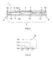
- FIG. 2 shows a luminous band for a lighting system according to the invention
- FIG. 3 shows a wiring diagram of a connection element according to the invention
- FIG. 4 shows a plug element as an example of a connection element according to the invention
- FIG. 5 shows a further plug element as an example of a connection element according to the invention
- FIG. 6 shows an illustration of a luminous band according to the invention.
- FIG. 1 shows a top view of a conventional flexible luminous band 1 consisting by way of example of two contiguous identical unit circuit boards 2 .
- Each of the unit circuit boards 2 has a flexible substrate 3 made of polyimide, the front side of which visible here is equipped with four light emitting diodes 4 .
- the light emitting diodes 4 are positioned evenly spaced (equidistantly) with respect to a longitudinal direction of the unit circuit board 2 .
- each of the unit circuit boards 2 has electrical contacts 5 , here: two contacts 5 in each case.
- the unit circuit boards 2 are manufactured integrally, whereby the substrates 3 of the unit circuit boards 2 are present as a single, one-piece quasi-continuous substrate of the luminous band 1 .
- the contacts 5 abutting against one another of two adjacent unit circuit boards 2 are implemented as a single contact strip which extends over both unit circuit boards 2 .
- the unit circuit boards 2 are interconnected electrically in parallel.
- a division between light emitting diodes 4 of a unit circuit board 2 has the consequence that all the light emitting diodes 4 of this unit circuit board 2 fail because the light emitting diodes 4 of one unit circuit board 2 are connected electrically in series.
- FIG. 1 shows a top view of a unit circuit board 2 in a detail view in accordance with the prior art.
- a pair of bridging contacts 6 in the form of soldering fields.
- Each of the pairs of bridging contacts 6 can for example be bridged by soldering-on a surface-mountable resistor (not illustrated).
- the unit circuit board 2 can be severed between two light emitting diodes 4 , for example along a dividing line U, more precisely between a pair of bridging contacts 6 and the light emitting diode 4 connected electrically downstream, here: arranged further to the right.
- FIG. 1 (bottom) shows a possible circuit diagram for the unit circuit board 2 .
- the unit circuit board 2 is equipped with a control circuit 7 which has two transistors Q 1 , Q 2 and two resistors R 1 , R 2 .
- the control circuit 7 is connected by way of the contacts 8 and/or 9 to an electrical supply (not illustrated).
- the light emitting diodes 4 are connected electrically in series downstream of the control circuit 7 . If the unit circuit board 2 is severed along the dividing lines U from FIG. 1 (top) without additional measures being taken, the circuit of this unit circuit board 2 will be interrupted, which means that none of the light emitting diodes 4 would be illuminated any longer.
- FIG. 2 shows a schematic top view of a unit circuit board 2 of a luminous band 1 for a lighting system according to the invention.
- the layout of the unit circuit board 2 is likewise shown schematically.
- the basic structure corresponds to the luminous band 2 shown in FIG. 1 , in other words each of the unit circuit boards 2 has electrical contacts 5 a , 5 b , here two contacts 5 a , 5 b in each case, at both (viewed with respect to the longitudinal direction) end areas E.
- the layout of the unit circuit board 2 essentially corresponds to the circuit diagram shown in FIG. 1 (bottom), whereby the control circuit 7 has not been included in the illustration.
- Two continuous conductor paths 10 , 11 are provided which can also be used for the power supply to downstream unit circuit boards 2 , such that the unit circuit boards 2 of a luminous band 1 are connected electrically in parallel.
- the LEDs 4 are connected in series by means of a conductor path 12 connecting the LEDs 4 .
- a contact area 13 is provided at which a first continuous conductor path 10 and also the conductor path 12 connecting the LEDs 4 are in each case provided with a contact 14 a , 14 b .
- the contacts 14 b of the continuous conductor path 10 (which naturally have approximately the same potential at all contact areas 13 ) are situated at the same position at all contact areas 13 viewed in the transverse direction of the luminous band 1 , whereas the position of the contact 14 a of the conductor path 12 connecting the LEDs 4 varies depending on the number of LEDs 4 between the dividing point T and the contacts 5 a for feeding current into the unit circuit board 2 .
- the distance between the contact 14 b of the continuous conductor path 10 and the contact 14 a of the conductor path 12 connecting the LEDs decreases, in other words as the number of severed LEDs 4 increases, the distance between the contact 14 b of the continuous conductor path 10 and the contact 14 a of the conductor path 12 connecting the LEDs 4 increases.
- connection element 15 This enables a particularly simple construction of the connection element 15 , the circuit diagram for which is shown by way of example in FIG. 3 .
- One contact 16 of the connection element 15 is provided for making contact with the contact 14 b of the continuous conductor path 10
- the contacts 17 are provided for making contact with the contacts 14 a of the conductor paths 12 connecting the LEDs 4 .
- the elements 18 represent electronic components 18 a which are required for closing a circuit of the luminous band 1 .
- One element 18 is provided in each case to compensate for the absence of an LED 4 , in other words the voltage drops at the element 18 to the same extent as at an LED 4 used on the luminous band 1 . If the distance between the contacts 14 a and 14 b decreases as the number of severed LEDs 4 increases (or increases as the number of operated LEDs 4 decreases), the connection element 15 can thus be configured without crossing conductor paths, which simplifies the manufacturing process.
- the elements 18 can for example consist of individual resistors or diodes or also of arrays of such electronic components 18 a .
- the use of resistors offers a simple and cost-effective variant if the luminous band is operated at a constant current in all application situations because the voltage drop at the resistor is then also clearly defined. If the connection element 15 is to be capable of being operated at different currents, the more elaborate use of diodes is advisable because these always exhibit the same voltage drop as would also occur at the severed LEDs 4 .
- FIG. 4 shows different embodiments of a connection element according to the invention.
- a connection element 15 is shown in FIG. 4 a which is essentially constructed from a so-called ZIF connector 19 , in other words a zero insertion force connection element 19 , with an FR 4 board 20 , in other words a board constructed from epoxy resin and glass fiber fabric, connected directly and fixedly thereto.
- the connection element 15 can be used in order to replace up to three severed LEDs 4 which are substituted by three diodes 21 as electronic components 18 a .
- the construction corresponds to the diagram shown in FIG. 3 .
- FIG. 4 b shows a connection element 15 identical to a large extent to that shown in FIG.
- connection cables 22 can thereby be extended beyond the connection element 15 by means of the connection cables 22 in order for example to be connected to further luminous bands 2 .
- FIG. 4 c shows a variant of the connection element 15 shown in FIG. 4 b , wherein a housing 23 encloses the board 20 , the diodes 21 and also in part the ZIF connector 19 and also the connection cables 22 .
- the housing 23 is implemented as an injection molded part which for the purpose of improved heat dissipation is filled with so-called seal gel, in other words a mass which is heat dissipating, electrically insulating and where necessary offers protection against moisture.
- seal gel in other words a mass which is heat dissipating, electrically insulating and where necessary offers protection against moisture.
- Other embodiments of the housing 23 are conceivable, both in respect of the design and the manufacture and also of the material used, for example in the form of an encapsulation or through application of a hot melt adhesive.
- FIG. 4 d shows a further exemplary embodiment of a connection element 15 according to the invention.
- the board 20 is implemented as a metal core printed circuit board which enables a better heat dissipation from the electronic components 18 a .
- the board 20 is not enclosed by the housing 23 on its underside and can thus be connected directly by means of an adhesive layer 24 to a heat sink (not illustrated here) which for example is also used for cooling the luminous band 1 .
- connection element A further embodiment of the connection element is shown schematically in FIG. 5 .
- a connector 19 is connected as a connection element 15 by means of a cable connection 25 to an electronics module 26 which contains the elements 18 required for closing the circuit and is in turn arranged on a heat sink 27 .
- This type of construction is particularly well suited if high power levels need to be dissipated since as a result of the spatial separation of the electronics module 26 from the luminous band 1 the thermal load on the latter can be considerably reduced.
- the connector 19 at the end of the luminous band 1 requires substantially less installation space than if an arrangement according to FIG. 4 is installed.
- FIG. 6 shows an exemplary embodiment of an inventive luminous band 1 , not yet equipped with components, in an overall view (bottom) and also in three detail views (top).
- On the rear side B of the luminous band 1 in other words on the side facing away from the LEDs 4 , two continuous conductor paths 28 , 29 are provided which can also be used for supplying power to downstream unit circuit boards 2 .
- On the front side A are arranged further conductor paths 10 , 11 , 12 which are provided primarily for supplying voltage to the LEDs. At the side in this situation are provided the continuous conductor paths 10 , 11 which can also be used for supplying power supply to downstream unit circuit boards.
- a contact area 13 is shown which has contacts 14 a of the conductor path 12 connecting the LEDs 4 and also contacts 14 b of the conductor path 10 .
- luminous bands in particular those where a relatively thin carrier material and relatively thick conductor paths are used, as in the present exemplary embodiment in which a polyimide film 25 ⁇ m thick is arranged between copper conductor paths 50 ⁇ m thick, it can happen when severing a dividing point T that the two copper layers come into contact with one another, which means that a short-circuit may result in the event of a difference in potential.
- the lower conductor paths 28 , 29 are provided with recesses 30 in the contact area 13 , such that they are spaced away there transversally from the contacts 14 a situated above which may have a different potential.
- Such a principle can be applied in the case of all luminous bands which are capable of being severed, irrespective of whether a connection element 15 or a soldered connection is used or even if no further processing whatsoever takes place.
- connection elements 15 can also be adapted by simple means to suit special circumstances of the applications.
- connection elements 15 with different types of luminous bands 1 , or else in the case of identical luminous bands 1 to use different connection elements 15 which for example are specifically designed for the intended use on the basis of their geometry, the components 18 a used or other features.
- the different embodiments in FIG. 4 each of which can be used with identical luminous bands 1 , can also serve as examples in this situation.
- the severing of the luminous band 1 can be effected for example by cutting, or by scoring and breaking.
- the circuit board 2 can, among other things, advantageously be flexible (‘flexband’) in order to also apply the luminous band 1 onto curved surfaces.
- laser diodes can also be used as the semiconductor light source.
- establishing contact for the luminous band 1 can also be effected by means of other suitable connection elements, in particular by means of a different connector or a clamping connection.
Landscapes
- Engineering & Computer Science (AREA)
- General Engineering & Computer Science (AREA)
- Led Device Packages (AREA)
- Fastening Of Light Sources Or Lamp Holders (AREA)
- Arrangement Of Elements, Cooling, Sealing, Or The Like Of Lighting Devices (AREA)
Applications Claiming Priority (4)
| Application Number | Priority Date | Filing Date | Title |
|---|---|---|---|
| DE102009019285A DE102009019285A1 (de) | 2009-04-30 | 2009-04-30 | Beleuchtungssystem mit mindestens einem Leuchtband |
| DE102009019285 | 2009-04-30 | ||
| DE102009019285.9 | 2009-04-30 | ||
| PCT/EP2010/055849 WO2010145879A1 (de) | 2009-04-30 | 2010-04-29 | Beleuchtungssystem mit mindestens einem leuchtband |
Publications (2)
| Publication Number | Publication Date |
|---|---|
| US20120044689A1 US20120044689A1 (en) | 2012-02-23 |
| US9228707B2 true US9228707B2 (en) | 2016-01-05 |
Family
ID=42543087
Family Applications (1)
| Application Number | Title | Priority Date | Filing Date |
|---|---|---|---|
| US13/266,473 Expired - Fee Related US9228707B2 (en) | 2009-04-30 | 2010-04-29 | Lighting system comprising at least one luminous band |
Country Status (5)
| Country | Link |
|---|---|
| US (1) | US9228707B2 (de) |
| EP (1) | EP2425176B1 (de) |
| CN (1) | CN102365491B (de) |
| DE (1) | DE102009019285A1 (de) |
| WO (1) | WO2010145879A1 (de) |
Families Citing this family (12)
| Publication number | Priority date | Publication date | Assignee | Title |
|---|---|---|---|---|
| GB201105499D0 (en) * | 2011-03-31 | 2011-05-18 | Juice Technology Ltd | Electrical device |
| DE102011075032A1 (de) | 2011-04-29 | 2012-10-31 | Osram Ag | Leuchtvorrichtung und Verfahren zum Herstellen einer Leuchtvorrichtung |
| EP2805101B1 (de) * | 2012-01-16 | 2016-08-31 | OSRAM GmbH | Beleuchtungsmodul |
| US9772076B2 (en) | 2013-09-30 | 2017-09-26 | Osram Sylvania Inc. | Cuttable flexible light engines |
| US9423116B2 (en) * | 2013-12-11 | 2016-08-23 | Cree, Inc. | LED lamp and modular lighting system |
| DE102014104433A1 (de) | 2014-03-28 | 2015-10-01 | Döllken-Kunststoffverarbeitung Gmbh | Verfahren und Vorrichtung zum Bearbeiten eines LED-Streifens |
| DE102014226893B3 (de) * | 2014-12-23 | 2016-05-12 | H4X E.U. | Ablängbare Einbauleuchte mit einem ablängbaren Leuchtmittelträger |
| MX375804B (es) | 2015-04-13 | 2025-03-07 | Hubbell Lighting Inc | Placa de iluminación. |
| DE102017106813B4 (de) | 2016-05-09 | 2018-01-18 | Elmos Semiconductor Aktiengesellschaft | Vorrichtung und zugehöriges Verfahren zur selbständigen Adresskonfiguration konfektionierbarer, flexibler Sensor-Bänder |
| DE102017106811B4 (de) | 2016-05-09 | 2018-01-11 | Elmos Semiconductor Aktiengesellschaft | Vorrichtung und zugehöriges Verfahren zur selbständigen Adresskonfiguration konfektionierbarer, flexibler LED-Bänder |
| DE102017106812B4 (de) | 2016-05-09 | 2018-01-11 | Elmos Semiconductor Aktiengesellschaft | Vorrichtung und zugehöriges Verfahren zur selbständigen Adresskonfiguration konfektionierbarer, flexibler LED-Sensor-Bänder |
| JP7464264B2 (ja) * | 2020-04-08 | 2024-04-09 | 株式会社オオサカネーム | 帯状基板および帯状led発光装置 |
Citations (18)
| Publication number | Priority date | Publication date | Assignee | Title |
|---|---|---|---|---|
| US4173035A (en) | 1977-12-01 | 1979-10-30 | Media Masters, Inc. | Tape strip for effecting moving light display |
| GB2095482A (en) | 1978-05-31 | 1982-09-29 | Ferranti Ltd | Low insertion force electrical connector |
| US5107408A (en) | 1988-03-31 | 1992-04-21 | Consumerville Limited | Lighting system |
| US5559681A (en) | 1994-05-13 | 1996-09-24 | Cnc Automation, Inc. | Flexible, self-adhesive, modular lighting system |
| FR2739524A1 (fr) | 1995-10-02 | 1997-04-04 | Aupem Sefli | Barrette de circuit imprime pour iodes electroluminescentes, profile support pour une telle barrette, luminaire et panneau lumineux |
| DE10051528A1 (de) | 2000-10-17 | 2002-05-02 | Vossloh Schwabe Elektronik | Modulares Beleuchtungssystem |
| US20030112627A1 (en) | 2000-09-28 | 2003-06-19 | Deese Raymond E. | Flexible sign illumination apparatus, system and method |
| US6659623B2 (en) * | 2000-05-05 | 2003-12-09 | Thales Optronics (Taunton) Ltd. | Illumination system |
| DE10319525A1 (de) | 2003-04-30 | 2004-11-25 | Lawson Mardon Singen Gmbh | Bandförmige Anordnung mit einer Leiterbahnstruktur und mit damit elektrisch verbundenen elektronischen Bauteilen, insbesondere Lichtband mit Leuchtelementen |
| DE202005006643U1 (de) | 2005-04-26 | 2005-09-08 | Fan, Ben, Hsitzu | Flexible LED-Kabel-Beleuchtung |
| CN2746249Y (zh) | 2004-12-01 | 2005-12-14 | 樊邦弘 | 柔性带灯结构 |
| US7140751B2 (en) * | 2004-03-24 | 2006-11-28 | Yuan Lin | Full-color flexible light source device |
| DE102007003609A1 (de) | 2006-06-06 | 2007-12-13 | Friebe, Michael, Dipl.-Ing. Dr. | Infusionschlauch für eine Pumpvorrichtung und Pumpvorrichtung |
| CN201000001Y (zh) | 2007-01-08 | 2008-01-02 | 赖金鸿 | 可调长度的led灯条 |
| CN201000000Y (zh) | 2007-01-08 | 2008-01-02 | 赖金鸿 | 可程序化全彩led灯条 |
| DE102007028463A1 (de) | 2007-06-18 | 2009-01-02 | Osram Gesellschaft mit beschränkter Haftung | Lichtemittierendes System mit Steckverbindung |
| DE102009008095A1 (de) | 2009-02-09 | 2010-08-12 | Osram Gesellschaft mit beschränkter Haftung | Konfektionierbares Leuchtband |
| DE102009014535A1 (de) | 2009-03-24 | 2010-09-30 | Osram Gesellschaft mit beschränkter Haftung | Leuchtmodul, Nullkraftverbindungselement und Stromversorgung für ein Leuchtband |
Family Cites Families (1)
| Publication number | Priority date | Publication date | Assignee | Title |
|---|---|---|---|---|
| DE102007003809B4 (de) * | 2006-09-27 | 2012-03-08 | Osram Ag | Verfahren zum Herstellen einer Leuchtdiodenanordnung und Leuchtdiodenanordnung mit einer Mehrzahl von kettenförmig angeordneten LED-Modulen |
-
2009
- 2009-04-30 DE DE102009019285A patent/DE102009019285A1/de not_active Withdrawn
-
2010
- 2010-04-29 US US13/266,473 patent/US9228707B2/en not_active Expired - Fee Related
- 2010-04-29 WO PCT/EP2010/055849 patent/WO2010145879A1/de not_active Ceased
- 2010-04-29 EP EP10720375.4A patent/EP2425176B1/de not_active Not-in-force
- 2010-04-29 CN CN201080014101.4A patent/CN102365491B/zh not_active Expired - Fee Related
Patent Citations (20)
| Publication number | Priority date | Publication date | Assignee | Title |
|---|---|---|---|---|
| US4173035A (en) | 1977-12-01 | 1979-10-30 | Media Masters, Inc. | Tape strip for effecting moving light display |
| GB2095482A (en) | 1978-05-31 | 1982-09-29 | Ferranti Ltd | Low insertion force electrical connector |
| US5107408A (en) | 1988-03-31 | 1992-04-21 | Consumerville Limited | Lighting system |
| DE68915200T2 (de) | 1988-03-31 | 1994-12-08 | Existalite Ltd | Dekorative Beleuchtungsvorrichtung. |
| US5559681A (en) | 1994-05-13 | 1996-09-24 | Cnc Automation, Inc. | Flexible, self-adhesive, modular lighting system |
| FR2739524A1 (fr) | 1995-10-02 | 1997-04-04 | Aupem Sefli | Barrette de circuit imprime pour iodes electroluminescentes, profile support pour une telle barrette, luminaire et panneau lumineux |
| US6659623B2 (en) * | 2000-05-05 | 2003-12-09 | Thales Optronics (Taunton) Ltd. | Illumination system |
| US20030112627A1 (en) | 2000-09-28 | 2003-06-19 | Deese Raymond E. | Flexible sign illumination apparatus, system and method |
| DE10051528A1 (de) | 2000-10-17 | 2002-05-02 | Vossloh Schwabe Elektronik | Modulares Beleuchtungssystem |
| DE10319525A1 (de) | 2003-04-30 | 2004-11-25 | Lawson Mardon Singen Gmbh | Bandförmige Anordnung mit einer Leiterbahnstruktur und mit damit elektrisch verbundenen elektronischen Bauteilen, insbesondere Lichtband mit Leuchtelementen |
| US7140751B2 (en) * | 2004-03-24 | 2006-11-28 | Yuan Lin | Full-color flexible light source device |
| CN2746249Y (zh) | 2004-12-01 | 2005-12-14 | 樊邦弘 | 柔性带灯结构 |
| DE202005006643U1 (de) | 2005-04-26 | 2005-09-08 | Fan, Ben, Hsitzu | Flexible LED-Kabel-Beleuchtung |
| DE102007003609A1 (de) | 2006-06-06 | 2007-12-13 | Friebe, Michael, Dipl.-Ing. Dr. | Infusionschlauch für eine Pumpvorrichtung und Pumpvorrichtung |
| CN201000001Y (zh) | 2007-01-08 | 2008-01-02 | 赖金鸿 | 可调长度的led灯条 |
| CN201000000Y (zh) | 2007-01-08 | 2008-01-02 | 赖金鸿 | 可程序化全彩led灯条 |
| DE102007028463A1 (de) | 2007-06-18 | 2009-01-02 | Osram Gesellschaft mit beschränkter Haftung | Lichtemittierendes System mit Steckverbindung |
| US7771204B2 (en) | 2007-06-18 | 2010-08-10 | Osram Gesellschaft mit beschränkter Haftung | Light-emitting system with a plug connection |
| DE102009008095A1 (de) | 2009-02-09 | 2010-08-12 | Osram Gesellschaft mit beschränkter Haftung | Konfektionierbares Leuchtband |
| DE102009014535A1 (de) | 2009-03-24 | 2010-09-30 | Osram Gesellschaft mit beschränkter Haftung | Leuchtmodul, Nullkraftverbindungselement und Stromversorgung für ein Leuchtband |
Non-Patent Citations (10)
| Title |
|---|
| English abstract for CN 201000000Y dated Jan. 2, 2008. |
| English abstract for CN 201000001Y dated Jan. 2, 2008. |
| English abstract for CN 2746249Y dated Dec. 14, 2005. |
| English abstract of DE 10051528 A1. |
| English abstract of DE 102007003809 A1. |
| English abstract of DE 102009008095 A1. |
| English Abstract of DE 102009014535 A1. |
| English Abstract of DE 10319525 A1. |
| English Abstract of DE 202005006643 U1. |
| English abstract of FR 2739524 A1. |
Also Published As
| Publication number | Publication date |
|---|---|
| CN102365491B (zh) | 2014-03-12 |
| CN102365491A (zh) | 2012-02-29 |
| EP2425176A1 (de) | 2012-03-07 |
| DE102009019285A1 (de) | 2010-11-04 |
| US20120044689A1 (en) | 2012-02-23 |
| EP2425176B1 (de) | 2016-08-24 |
| WO2010145879A1 (de) | 2010-12-23 |
Similar Documents
| Publication | Publication Date | Title |
|---|---|---|
| US9228707B2 (en) | Lighting system comprising at least one luminous band | |
| US7898811B2 (en) | Thermal management of LEDs on a printed circuit board and associated methods | |
| US8398261B2 (en) | Lighting strips with improved manufacturability | |
| US9941258B2 (en) | LED lead frame array for general illumination | |
| CN110431664B (zh) | 将led元件安装在平的载体上 | |
| US20110180819A1 (en) | Light-emitting arrangement | |
| JP4724700B2 (ja) | 発光装置 | |
| EP2188849B1 (de) | Lichtemittierendes bauelement | |
| US9249961B2 (en) | Light-emitting device | |
| US11277906B2 (en) | Separable modules PCB modules | |
| US8552450B2 (en) | LED package structure with a fuse for protection from high current | |
| KR101745222B1 (ko) | 점멸기 | |
| WO2009068867A1 (en) | Junction box | |
| US10383209B2 (en) | Electronic assembly for lighting applications, lighting device and method for producing an electronic assembly | |
| ES2943137T3 (es) | Circuito de alta corriente | |
| KR102458620B1 (ko) | Led 조명 디바이스 | |
| JP3789428B2 (ja) | 発光装置 | |
| KR101146096B1 (ko) | Led 패키지, 이를 이용한 발광 유닛 및 측면 발광형 백 라이트 유닛 | |
| CN101816107B (zh) | 电路保护器和电连接盒 | |
| US20210126513A1 (en) | Power conversion device and power conversion device-integrated rotary electric machine | |
| US20240274544A1 (en) | Semiconductor module and semiconductor device | |
| JP2011258313A (ja) | 電線接続装置および照明器具 | |
| US20080191594A1 (en) | Electroluminescent Device | |
| EP3297409B1 (de) | Verfahren zur verbindung von beleuchtungsmodulen und zugehörige vorrichtung | |
| JP2017054689A (ja) | Ledモジュール及び照明装置 |
Legal Events
| Date | Code | Title | Description |
|---|---|---|---|
| AS | Assignment |
Owner name: OSRAM AG, GERMANY Free format text: ASSIGNMENT OF ASSIGNORS INTEREST;ASSIGNORS:KRAUS, ROBERT;PREUSCHL, THOMAS;STRAUSS, STEFFEN;AND OTHERS;SIGNING DATES FROM 20110823 TO 20110912;REEL/FRAME:027130/0163 |
|
| AS | Assignment |
Owner name: OSRAM GMBH, GERMANY Free format text: CHANGE IN LEGAL FORM;ASSIGNOR:OSRAM AG;REEL/FRAME:035571/0371 Effective date: 20121025 |
|
| FEPP | Fee payment procedure |
Free format text: PAYOR NUMBER ASSIGNED (ORIGINAL EVENT CODE: ASPN); ENTITY STATUS OF PATENT OWNER: LARGE ENTITY |
|
| STCF | Information on status: patent grant |
Free format text: PATENTED CASE |
|
| FEPP | Fee payment procedure |
Free format text: MAINTENANCE FEE REMINDER MAILED (ORIGINAL EVENT CODE: REM.); ENTITY STATUS OF PATENT OWNER: LARGE ENTITY |
|
| LAPS | Lapse for failure to pay maintenance fees |
Free format text: PATENT EXPIRED FOR FAILURE TO PAY MAINTENANCE FEES (ORIGINAL EVENT CODE: EXP.); ENTITY STATUS OF PATENT OWNER: LARGE ENTITY |
|
| STCH | Information on status: patent discontinuation |
Free format text: PATENT EXPIRED DUE TO NONPAYMENT OF MAINTENANCE FEES UNDER 37 CFR 1.362 |
|
| FP | Lapsed due to failure to pay maintenance fee |
Effective date: 20200105 |