US9097754B2 - Method of manufacturing magnetoresistive element - Google Patents
Method of manufacturing magnetoresistive element Download PDFInfo
- Publication number
- US9097754B2 US9097754B2 US13/748,665 US201313748665A US9097754B2 US 9097754 B2 US9097754 B2 US 9097754B2 US 201313748665 A US201313748665 A US 201313748665A US 9097754 B2 US9097754 B2 US 9097754B2
- Authority
- US
- United States
- Prior art keywords
- layer
- magnetic layer
- insulating layer
- magnetoresistive element
- manufacturing
- Prior art date
- Legal status (The legal status is an assumption and is not a legal conclusion. Google has not performed a legal analysis and makes no representation as to the accuracy of the status listed.)
- Active, expires
Links
- 238000004519 manufacturing process Methods 0.000 title claims abstract description 49
- 238000000034 method Methods 0.000 claims abstract description 85
- 238000001020 plasma etching Methods 0.000 claims abstract description 18
- 239000000758 substrate Substances 0.000 claims abstract description 17
- 230000004888 barrier function Effects 0.000 claims abstract description 14
- 239000000463 material Substances 0.000 claims description 61
- 230000005415 magnetization Effects 0.000 claims description 29
- 229910019236 CoFeB Inorganic materials 0.000 claims description 14
- 238000004544 sputter deposition Methods 0.000 claims description 14
- 238000002347 injection Methods 0.000 claims description 13
- 239000007924 injection Substances 0.000 claims description 13
- OKKJLVBELUTLKV-UHFFFAOYSA-N Methanol Chemical compound OC OKKJLVBELUTLKV-UHFFFAOYSA-N 0.000 claims description 9
- 239000011810 insulating material Substances 0.000 claims description 4
- VNWKTOKETHGBQD-UHFFFAOYSA-N methane Natural products C VNWKTOKETHGBQD-UHFFFAOYSA-N 0.000 claims 1
- 239000010410 layer Substances 0.000 description 321
- 238000005530 etching Methods 0.000 description 47
- 239000007789 gas Substances 0.000 description 47
- 230000008569 process Effects 0.000 description 32
- 239000000395 magnesium oxide Substances 0.000 description 22
- CPLXHLVBOLITMK-UHFFFAOYSA-N magnesium oxide Inorganic materials [Mg]=O CPLXHLVBOLITMK-UHFFFAOYSA-N 0.000 description 22
- AXZKOIWUVFPNLO-UHFFFAOYSA-N magnesium;oxygen(2-) Chemical compound [O-2].[Mg+2] AXZKOIWUVFPNLO-UHFFFAOYSA-N 0.000 description 22
- 230000003647 oxidation Effects 0.000 description 10
- 238000007254 oxidation reaction Methods 0.000 description 10
- 230000015572 biosynthetic process Effects 0.000 description 9
- TWNQGVIAIRXVLR-UHFFFAOYSA-N oxo(oxoalumanyloxy)alumane Chemical compound O=[Al]O[Al]=O TWNQGVIAIRXVLR-UHFFFAOYSA-N 0.000 description 9
- 238000010586 diagram Methods 0.000 description 8
- 150000002500 ions Chemical class 0.000 description 8
- 229910052756 noble gas Inorganic materials 0.000 description 6
- 150000002835 noble gases Chemical class 0.000 description 6
- CNQCVBJFEGMYDW-UHFFFAOYSA-N lawrencium atom Chemical compound [Lr] CNQCVBJFEGMYDW-UHFFFAOYSA-N 0.000 description 5
- IJGRMHOSHXDMSA-UHFFFAOYSA-N Atomic nitrogen Chemical compound N#N IJGRMHOSHXDMSA-UHFFFAOYSA-N 0.000 description 4
- QVGXLLKOCUKJST-UHFFFAOYSA-N atomic oxygen Chemical compound [O] QVGXLLKOCUKJST-UHFFFAOYSA-N 0.000 description 4
- 239000011777 magnesium Substances 0.000 description 4
- 229910052751 metal Inorganic materials 0.000 description 4
- 239000002184 metal Substances 0.000 description 4
- 229910052760 oxygen Inorganic materials 0.000 description 4
- 239000001301 oxygen Substances 0.000 description 4
- 229910020068 MgAl Inorganic materials 0.000 description 3
- ATJFFYVFTNAWJD-UHFFFAOYSA-N Tin Chemical compound [Sn] ATJFFYVFTNAWJD-UHFFFAOYSA-N 0.000 description 3
- 230000008878 coupling Effects 0.000 description 3
- 238000010168 coupling process Methods 0.000 description 3
- 238000005859 coupling reaction Methods 0.000 description 3
- 230000000694 effects Effects 0.000 description 3
- 238000009616 inductively coupled plasma Methods 0.000 description 3
- 239000011229 interlayer Substances 0.000 description 3
- 239000000696 magnetic material Substances 0.000 description 3
- 239000000203 mixture Substances 0.000 description 3
- 230000035515 penetration Effects 0.000 description 3
- 230000000087 stabilizing effect Effects 0.000 description 3
- CBENFWSGALASAD-UHFFFAOYSA-N Ozone Chemical compound [O-][O+]=O CBENFWSGALASAD-UHFFFAOYSA-N 0.000 description 2
- 229910010038 TiAl Inorganic materials 0.000 description 2
- 229910008484 TiSi Inorganic materials 0.000 description 2
- 229910052786 argon Inorganic materials 0.000 description 2
- 229910052799 carbon Inorganic materials 0.000 description 2
- 230000008859 change Effects 0.000 description 2
- 230000002542 deteriorative effect Effects 0.000 description 2
- 238000009792 diffusion process Methods 0.000 description 2
- 238000001312 dry etching Methods 0.000 description 2
- 238000005516 engineering process Methods 0.000 description 2
- 229910052734 helium Inorganic materials 0.000 description 2
- 229910052743 krypton Inorganic materials 0.000 description 2
- 229910052754 neon Inorganic materials 0.000 description 2
- 229910052757 nitrogen Inorganic materials 0.000 description 2
- QJGQUHMNIGDVPM-UHFFFAOYSA-N nitrogen group Chemical group [N] QJGQUHMNIGDVPM-UHFFFAOYSA-N 0.000 description 2
- 230000001590 oxidative effect Effects 0.000 description 2
- 229910052724 xenon Inorganic materials 0.000 description 2
- 229910001030 Iron–nickel alloy Inorganic materials 0.000 description 1
- 238000009825 accumulation Methods 0.000 description 1
- 238000004364 calculation method Methods 0.000 description 1
- 238000006243 chemical reaction Methods 0.000 description 1
- 230000007423 decrease Effects 0.000 description 1
- 230000001747 exhibiting effect Effects 0.000 description 1
- 238000002474 experimental method Methods 0.000 description 1
- 230000006870 function Effects 0.000 description 1
- 238000010884 ion-beam technique Methods 0.000 description 1
- 238000012986 modification Methods 0.000 description 1
- 230000004048 modification Effects 0.000 description 1
- 230000000149 penetrating effect Effects 0.000 description 1
- 238000003672 processing method Methods 0.000 description 1
- 230000009467 reduction Effects 0.000 description 1
- 239000004065 semiconductor Substances 0.000 description 1
- 230000001629 suppression Effects 0.000 description 1
Images


Classifications
-
- H—ELECTRICITY
- H10—SEMICONDUCTOR DEVICES; ELECTRIC SOLID-STATE DEVICES NOT OTHERWISE PROVIDED FOR
- H10N—ELECTRIC SOLID-STATE DEVICES NOT OTHERWISE PROVIDED FOR
- H10N50/00—Galvanomagnetic devices
- H10N50/10—Magnetoresistive devices
-
- G—PHYSICS
- G01—MEASURING; TESTING
- G01R—MEASURING ELECTRIC VARIABLES; MEASURING MAGNETIC VARIABLES
- G01R33/00—Arrangements or instruments for measuring magnetic variables
- G01R33/02—Measuring direction or magnitude of magnetic fields or magnetic flux
- G01R33/06—Measuring direction or magnitude of magnetic fields or magnetic flux using galvano-magnetic devices
- G01R33/09—Magnetoresistive devices
- G01R33/093—Magnetoresistive devices using multilayer structures, e.g. giant magnetoresistance sensors
-
- B—PERFORMING OPERATIONS; TRANSPORTING
- B44—DECORATIVE ARTS
- B44C—PRODUCING DECORATIVE EFFECTS; MOSAICS; TARSIA WORK; PAPERHANGING
- B44C1/00—Processes, not specifically provided for elsewhere, for producing decorative surface effects
- B44C1/22—Removing surface-material, e.g. by engraving, by etching
- B44C1/227—Removing surface-material, e.g. by engraving, by etching by etching
-
- C—CHEMISTRY; METALLURGY
- C23—COATING METALLIC MATERIAL; COATING MATERIAL WITH METALLIC MATERIAL; CHEMICAL SURFACE TREATMENT; DIFFUSION TREATMENT OF METALLIC MATERIAL; COATING BY VACUUM EVAPORATION, BY SPUTTERING, BY ION IMPLANTATION OR BY CHEMICAL VAPOUR DEPOSITION, IN GENERAL; INHIBITING CORROSION OF METALLIC MATERIAL OR INCRUSTATION IN GENERAL
- C23C—COATING METALLIC MATERIAL; COATING MATERIAL WITH METALLIC MATERIAL; SURFACE TREATMENT OF METALLIC MATERIAL BY DIFFUSION INTO THE SURFACE, BY CHEMICAL CONVERSION OR SUBSTITUTION; COATING BY VACUUM EVAPORATION, BY SPUTTERING, BY ION IMPLANTATION OR BY CHEMICAL VAPOUR DEPOSITION, IN GENERAL
- C23C16/00—Chemical coating by decomposition of gaseous compounds, without leaving reaction products of surface material in the coating, i.e. chemical vapour deposition [CVD] processes
- C23C16/22—Chemical coating by decomposition of gaseous compounds, without leaving reaction products of surface material in the coating, i.e. chemical vapour deposition [CVD] processes characterised by the deposition of inorganic material, other than metallic material
- C23C16/30—Deposition of compounds, mixtures or solid solutions, e.g. borides, carbides, nitrides
- C23C16/301—AIII BV compounds, where A is Al, Ga, In or Tl and B is N, P, As, Sb or Bi
-
- C—CHEMISTRY; METALLURGY
- C30—CRYSTAL GROWTH
- C30B—SINGLE-CRYSTAL GROWTH; UNIDIRECTIONAL SOLIDIFICATION OF EUTECTIC MATERIAL OR UNIDIRECTIONAL DEMIXING OF EUTECTOID MATERIAL; REFINING BY ZONE-MELTING OF MATERIAL; PRODUCTION OF A HOMOGENEOUS POLYCRYSTALLINE MATERIAL WITH DEFINED STRUCTURE; SINGLE CRYSTALS OR HOMOGENEOUS POLYCRYSTALLINE MATERIAL WITH DEFINED STRUCTURE; AFTER-TREATMENT OF SINGLE CRYSTALS OR A HOMOGENEOUS POLYCRYSTALLINE MATERIAL WITH DEFINED STRUCTURE; APPARATUS THEREFOR
- C30B29/00—Single crystals or homogeneous polycrystalline material with defined structure characterised by the material or by their shape
- C30B29/10—Inorganic compounds or compositions
- C30B29/40—AIIIBV compounds wherein A is B, Al, Ga, In or Tl and B is N, P, As, Sb or Bi
-
- G—PHYSICS
- G01—MEASURING; TESTING
- G01R—MEASURING ELECTRIC VARIABLES; MEASURING MAGNETIC VARIABLES
- G01R33/00—Arrangements or instruments for measuring magnetic variables
- G01R33/02—Measuring direction or magnitude of magnetic fields or magnetic flux
- G01R33/06—Measuring direction or magnitude of magnetic fields or magnetic flux using galvano-magnetic devices
- G01R33/09—Magnetoresistive devices
-
- G—PHYSICS
- G11—INFORMATION STORAGE
- G11C—STATIC STORES
- G11C11/00—Digital stores characterised by the use of particular electric or magnetic storage elements; Storage elements therefor
- G11C11/02—Digital stores characterised by the use of particular electric or magnetic storage elements; Storage elements therefor using magnetic elements
- G11C11/14—Digital stores characterised by the use of particular electric or magnetic storage elements; Storage elements therefor using magnetic elements using thin-film elements
- G11C11/15—Digital stores characterised by the use of particular electric or magnetic storage elements; Storage elements therefor using magnetic elements using thin-film elements using multiple magnetic layers
-
- G—PHYSICS
- G11—INFORMATION STORAGE
- G11C—STATIC STORES
- G11C11/00—Digital stores characterised by the use of particular electric or magnetic storage elements; Storage elements therefor
- G11C11/02—Digital stores characterised by the use of particular electric or magnetic storage elements; Storage elements therefor using magnetic elements
- G11C11/16—Digital stores characterised by the use of particular electric or magnetic storage elements; Storage elements therefor using magnetic elements using elements in which the storage effect is based on magnetic spin effect
- G11C11/161—Digital stores characterised by the use of particular electric or magnetic storage elements; Storage elements therefor using magnetic elements using elements in which the storage effect is based on magnetic spin effect details concerning the memory cell structure, e.g. the layers of the ferromagnetic memory cell
-
- H—ELECTRICITY
- H01—ELECTRIC ELEMENTS
- H01F—MAGNETS; INDUCTANCES; TRANSFORMERS; SELECTION OF MATERIALS FOR THEIR MAGNETIC PROPERTIES
- H01F41/00—Apparatus or processes specially adapted for manufacturing or assembling magnets, inductances or transformers; Apparatus or processes specially adapted for manufacturing materials characterised by their magnetic properties
- H01F41/14—Apparatus or processes specially adapted for manufacturing or assembling magnets, inductances or transformers; Apparatus or processes specially adapted for manufacturing materials characterised by their magnetic properties for applying magnetic films to substrates
- H01F41/30—Apparatus or processes specially adapted for manufacturing or assembling magnets, inductances or transformers; Apparatus or processes specially adapted for manufacturing materials characterised by their magnetic properties for applying magnetic films to substrates for applying nanostructures, e.g. by molecular beam epitaxy [MBE]
- H01F41/302—Apparatus or processes specially adapted for manufacturing or assembling magnets, inductances or transformers; Apparatus or processes specially adapted for manufacturing materials characterised by their magnetic properties for applying magnetic films to substrates for applying nanostructures, e.g. by molecular beam epitaxy [MBE] for applying spin-exchange-coupled multilayers, e.g. nanostructured superlattices
- H01F41/308—Apparatus or processes specially adapted for manufacturing or assembling magnets, inductances or transformers; Apparatus or processes specially adapted for manufacturing materials characterised by their magnetic properties for applying magnetic films to substrates for applying nanostructures, e.g. by molecular beam epitaxy [MBE] for applying spin-exchange-coupled multilayers, e.g. nanostructured superlattices lift-off processes, e.g. ion milling, for trimming or patterning
-
- H—ELECTRICITY
- H01—ELECTRIC ELEMENTS
- H01J—ELECTRIC DISCHARGE TUBES OR DISCHARGE LAMPS
- H01J37/00—Discharge tubes with provision for introducing objects or material to be exposed to the discharge, e.g. for the purpose of examination or processing thereof
- H01J37/32—Gas-filled discharge tubes
- H01J37/32009—Arrangements for generation of plasma specially adapted for examination or treatment of objects, e.g. plasma sources
- H01J37/32192—Microwave generated discharge
-
- H—ELECTRICITY
- H01—ELECTRIC ELEMENTS
- H01L—SEMICONDUCTOR DEVICES NOT COVERED BY CLASS H10
- H01L21/00—Processes or apparatus adapted for the manufacture or treatment of semiconductor or solid state devices or of parts thereof
- H01L21/02—Manufacture or treatment of semiconductor devices or of parts thereof
- H01L21/04—Manufacture or treatment of semiconductor devices or of parts thereof the devices having potential barriers, e.g. a PN junction, depletion layer or carrier concentration layer
- H01L21/18—Manufacture or treatment of semiconductor devices or of parts thereof the devices having potential barriers, e.g. a PN junction, depletion layer or carrier concentration layer the devices having semiconductor bodies comprising elements of Group IV of the Periodic Table or AIIIBV compounds with or without impurities, e.g. doping materials
- H01L21/30—Treatment of semiconductor bodies using processes or apparatus not provided for in groups H01L21/20 - H01L21/26
- H01L21/31—Treatment of semiconductor bodies using processes or apparatus not provided for in groups H01L21/20 - H01L21/26 to form insulating layers thereon, e.g. for masking or by using photolithographic techniques; After treatment of these layers; Selection of materials for these layers
- H01L21/3105—After-treatment
- H01L21/311—Etching the insulating layers by chemical or physical means
- H01L21/31127—Etching organic layers
- H01L21/31133—Etching organic layers by chemical means
- H01L21/31138—Etching organic layers by chemical means by dry-etching
-
- H01L43/12—
-
- H—ELECTRICITY
- H10—SEMICONDUCTOR DEVICES; ELECTRIC SOLID-STATE DEVICES NOT OTHERWISE PROVIDED FOR
- H10N—ELECTRIC SOLID-STATE DEVICES NOT OTHERWISE PROVIDED FOR
- H10N50/00—Galvanomagnetic devices
- H10N50/01—Manufacture or treatment
-
- B—PERFORMING OPERATIONS; TRANSPORTING
- B82—NANOTECHNOLOGY
- B82Y—SPECIFIC USES OR APPLICATIONS OF NANOSTRUCTURES; MEASUREMENT OR ANALYSIS OF NANOSTRUCTURES; MANUFACTURE OR TREATMENT OF NANOSTRUCTURES
- B82Y25/00—Nanomagnetism, e.g. magnetoimpedance, anisotropic magnetoresistance, giant magnetoresistance or tunneling magnetoresistance
-
- G—PHYSICS
- G11—INFORMATION STORAGE
- G11B—INFORMATION STORAGE BASED ON RELATIVE MOVEMENT BETWEEN RECORD CARRIER AND TRANSDUCER
- G11B5/00—Recording by magnetisation or demagnetisation of a record carrier; Reproducing by magnetic means; Record carriers therefor
- G11B5/127—Structure or manufacture of heads, e.g. inductive
- G11B5/31—Structure or manufacture of heads, e.g. inductive using thin films
- G11B5/3109—Details
- G11B5/3116—Shaping of layers, poles or gaps for improving the form of the electrical signal transduced, e.g. for shielding, contour effect, equalizing, side flux fringing, cross talk reduction between heads or between heads and information tracks
-
- H—ELECTRICITY
- H01—ELECTRIC ELEMENTS
- H01F—MAGNETS; INDUCTANCES; TRANSFORMERS; SELECTION OF MATERIALS FOR THEIR MAGNETIC PROPERTIES
- H01F41/00—Apparatus or processes specially adapted for manufacturing or assembling magnets, inductances or transformers; Apparatus or processes specially adapted for manufacturing materials characterised by their magnetic properties
- H01F41/14—Apparatus or processes specially adapted for manufacturing or assembling magnets, inductances or transformers; Apparatus or processes specially adapted for manufacturing materials characterised by their magnetic properties for applying magnetic films to substrates
- H01F41/30—Apparatus or processes specially adapted for manufacturing or assembling magnets, inductances or transformers; Apparatus or processes specially adapted for manufacturing materials characterised by their magnetic properties for applying magnetic films to substrates for applying nanostructures, e.g. by molecular beam epitaxy [MBE]
- H01F41/302—Apparatus or processes specially adapted for manufacturing or assembling magnets, inductances or transformers; Apparatus or processes specially adapted for manufacturing materials characterised by their magnetic properties for applying magnetic films to substrates for applying nanostructures, e.g. by molecular beam epitaxy [MBE] for applying spin-exchange-coupled multilayers, e.g. nanostructured superlattices
- H01F41/305—Apparatus or processes specially adapted for manufacturing or assembling magnets, inductances or transformers; Apparatus or processes specially adapted for manufacturing materials characterised by their magnetic properties for applying magnetic films to substrates for applying nanostructures, e.g. by molecular beam epitaxy [MBE] for applying spin-exchange-coupled multilayers, e.g. nanostructured superlattices applying the spacer or adjusting its interface, e.g. in order to enable particular effect different from exchange coupling
- H01F41/307—Apparatus or processes specially adapted for manufacturing or assembling magnets, inductances or transformers; Apparatus or processes specially adapted for manufacturing materials characterised by their magnetic properties for applying magnetic films to substrates for applying nanostructures, e.g. by molecular beam epitaxy [MBE] for applying spin-exchange-coupled multilayers, e.g. nanostructured superlattices applying the spacer or adjusting its interface, e.g. in order to enable particular effect different from exchange coupling insulating or semiconductive spacer
-
- H—ELECTRICITY
- H01—ELECTRIC ELEMENTS
- H01J—ELECTRIC DISCHARGE TUBES OR DISCHARGE LAMPS
- H01J37/00—Discharge tubes with provision for introducing objects or material to be exposed to the discharge, e.g. for the purpose of examination or processing thereof
- H01J37/32—Gas-filled discharge tubes
- H01J37/32009—Arrangements for generation of plasma specially adapted for examination or treatment of objects, e.g. plasma sources
- H01J37/32192—Microwave generated discharge
- H01J37/32211—Means for coupling power to the plasma
- H01J37/32229—Waveguides
-
- H—ELECTRICITY
- H01—ELECTRIC ELEMENTS
- H01L—SEMICONDUCTOR DEVICES NOT COVERED BY CLASS H10
- H01L21/00—Processes or apparatus adapted for the manufacture or treatment of semiconductor or solid state devices or of parts thereof
- H01L21/02—Manufacture or treatment of semiconductor devices or of parts thereof
- H01L21/04—Manufacture or treatment of semiconductor devices or of parts thereof the devices having potential barriers, e.g. a PN junction, depletion layer or carrier concentration layer
- H01L21/18—Manufacture or treatment of semiconductor devices or of parts thereof the devices having potential barriers, e.g. a PN junction, depletion layer or carrier concentration layer the devices having semiconductor bodies comprising elements of Group IV of the Periodic Table or AIIIBV compounds with or without impurities, e.g. doping materials
- H01L21/30—Treatment of semiconductor bodies using processes or apparatus not provided for in groups H01L21/20 - H01L21/26
- H01L21/302—Treatment of semiconductor bodies using processes or apparatus not provided for in groups H01L21/20 - H01L21/26 to change their surface-physical characteristics or shape, e.g. etching, polishing, cutting
- H01L21/306—Chemical or electrical treatment, e.g. electrolytic etching
- H01L21/3065—Plasma etching; Reactive-ion etching
Definitions
- the present invention relates to a method for manufacturing a magnetoresistive element.
- DRAM dynamic random access memory
- flash memory a non-volatile memory
- MRAM magnetoresistive random access memory
- FIG. 1A illustrates a basic structure of a magnetoresistive memory.
- the magnetoresistive memory includes a magnetoresistive element 103 that is disposed between a bit line 101 and a word line 102 , and a transistor 104 for selecting each resistive element.
- the magnetoresistive element 103 has a structure in which an insulating layer 107 is interposed between a free layer 105 that is a magnetic layer of which the magnetization direction can be inverted by external magnetic field or spin injection and a fixed layer 106 that is a magnetic film of which the magnetization direction is in a fixed state, and as illustrated in FIG.
- a memory in which a difference in electric resistance of the magnetoresistive element 103 corresponds to a 1.0 signal is a magnetoresistive memory and manufacturing of the magnetoresistive element that is a core part is important.
- the magnetization directions of the free layer 105 and the fixed layer 106 may horizontally face a film surface, but may vertically face the film surface.
- a film structure or a manufacturing method of the magnetoresistive element has been developed, and S. Ikeda et al., “Tunnel magnetoresistance of 604% at 300K by suppression of Ta diffusion in CoFeB/MgO/CoFeB pseudo spin-valves annealed at high temperature” Appl. Phys. Lett. 93 (2008) 082508 discloses a result in which the MR ratio of 604% is achieved.
- the magnetoresistive element in addition to the magnetoresistive memory, a magnetic head, a magnetic sensor, and the like, using the magnetoresistive element has been developed rapidly.
- a technology of fine processing an insulating layer made of magnetic materials including elements, such as Fe, Co, Ni, and the like, that are used for the free layer or the fixed layer or magnesium oxide (MgO), aluminum oxide (AlO), and the like, by dry etching is required.
- the dry etching method a method of using ion beam etching and a method of using plasma etching have been used.
- the plasma etching has been widely used for the manufacturing of the semiconductor device, and it has excellent productivity in that a large diameter substrate may be etched uniformly.
- the plasma etching has characteristics of improving a selection ratio for various hard mask materials by using chemical reaction.
- the plasma etching is carried out by introducing process gases into a decompressed process chamber and applying high frequency power (hereinafter, referred to as source power) from a source power supply to the process chamber via a flat antenna, a coil-shaped antenna, and the like, so as to generate a plasma of the process gases and to irradiate ions or radicals generated in the plasma to a substrate.
- source power high frequency power
- An example of the plasma source may include several types, such as an effective magnetic field microwave type, an inductively coupled plasma (ICP) type, a capacitively coupled plasma (CCP) type, and the like, according to a difference in types generating plasma.
- wafer bias power the high frequency power (hereinafter, referred to as wafer bias power) is applied even to a stage on which the wafer is disposed.
- the method using a plasma of Ar gas K. Kinoshita et al. “Etching Magnetic Tunnel Junction with Metal Etchers” Jpn. J. Appl. Phys. 49 (2010) 08JB02.
- the method using a plasma of mixed gas of CO and NH 3 Japanese Patent No. 02677321
- the method using a plasma of CH 3 OH gas Japanese Patent No. 04111274
- FIG. 2 illustrates an example of the method of processing a magnetoresistive element using the plasma etching.
- reference numeral 201 represents a Si substrate
- reference numeral 202 represents an electrode film
- reference numeral 203 represents an underlayer for controlling crystallinity of a fixed layer or stabilizing a magnetization of the fixed layer
- reference numeral 204 represents a fixed layer
- reference numeral 205 represents an insulating layer
- reference numeral 206 is a free layer
- reference numeral 207 represents a cap layer for protecting the free layer
- reference numeral 208 represents a hard mask
- reference numeral 209 represents a resist mask.
- transistors for selecting each resistive element or wirings for coupling each element are formed between the Si substrate 201 and the electrode film 202 . Further, there is a case in which the underlayer 203 or the cap layer 207 is not present.
- As one of the processing methods of the magnetoresistive element there is a method, as illustrated in the left drawing of FIG. 2 , of forming each layer, etching the hard mask layer 208 and the cap layer 207 in the process ( 1 ) shown in FIG. 2 , and etching only the free layer 206 in the process ( 2 ) shown in FIG. 2 . In this method, it is particularly important to etch only the free layer 206 during the process of FIG. 2 ( 2 ).
- K. Kinoshita et al. “Etching Magnetic Tunnel Junction with Metal Etchers” Jpn. J. Appl. Phys. 49 (2010) 08JB02 reports a result of etching only the free layer 206 using Ar plasma.
- a sub trench 301 formed during the over etching penetrates through a part of the insulating layer 205 thereunder, the characteristics of the magnetoresistive element largely deteriorate. Therefore, in order to manufacture the magnetoresistive element showing good characteristics on the overall surface of the wafer, a need exists for a technology of etching only the free layer on the overall surface of the wafer.
- etching only the free layer on the overall surface of the wafer there is a method of making an etching rate on the overall surface of the wafer uniform and etching only the free layer in all the elements within the wafer surface by the processing for a predetermined time.
- a method for improving both in terms of process and hardware of an etching apparatus has been studied.
- Table 1 shows results of measuring a selection ratio of the insulating layer to the free layer according to a kind of gases by using CoFeB as a representative free layer and MgO as a representative insulating layer.
- the selection ratio of the insulating layer is defined by the following Equation and as the selection ratio of the insulating layer is increased, it is shown that the etching rate of the insulating layer is slower than the etching rate of the free layer.
- Selection ratio of insulating layer etching rate of free layer (nm/min)/etching rate of insulating layer (nm/min) [Equation 2]
- each selection ratio is calculated from results of etching the free layer of CoFeB and the insulating layer of MgO by changing a kind of gases using an ICP type of plasma source under the following etching conditions.
- the selection ratio in all kinds of gases examined is 3 or less.
- the process conditions such as the process pressure, the source power, the wafer bias power are examined based on etching condition 1, but the selection ratio of the insulating layer cannot be largely improved. Therefore, a new method of improving the selection ratio of the insulating layer is needed.
- the present invention is directed to provide a method for manufacturing a magnetoresistive element having an etching rate of an insulating layer slower than that of a free layer (magnetic layer), that is, a high selection ratio of the insulating layer to the free layer so as to prevent a characteristic of the magnetoresistive element from deteriorating due to a penetration of a part of the insulating layer just under the free layer.
- a method for manufacturing a magnetoresistive element includes the steps of: preparing a substrate on which a first magnetic layer, a second magnetic layer disposed under the first magnetic layer, and a barrier layer that is an insulating layer disposed between the first magnetic layer and the second magnetic layer are formed; and processing the first magnetic layer by plasma etching, in which the barrier layer contains a Ta element or a Ti element.
- a method for manufacturing a magnetoresistive element includes the steps of: forming a second magnetic layer over a substrate; forming a barrier layer that is an insulating layer containing a Ta element or a Ti element on the second magnetic layer by sputtering an insulating material target and a Ta-containing material target or a Ti-containing material target that configure an insulating layer; forming a first magnetic layer on the barrier layer; and processing the first magnetic layer by plasma etching.
- the present invention it is possible to provide the method for manufacturing a magnetoresistive element having the high selection ratio of the insulating layer to the free layer.
- FIGS. 1A and 1B are schematic diagrams for describing a basic operation principle of a magnetoresistive element, in which FIG. 1A illustrates a case in which a magnetization direction of a fixed layer is the same as a magnetization direction of a free layer and FIG. 1B illustrates a case in which the magnetization directions of the fixed layer and the free layer are opposite to each other;
- FIG. 2 is a schematic diagram illustrating a process flow of etching the free layer of the magnetoresistive element by plasma etching
- FIGS. 3A and 3B are schematic diagrams for describing a problem when the free layer of the magnetoresistive element is etched by the plasma etching, in which FIG. 3A illustrates a case in which the etching of the free layer is insufficient and FIG. 3B illustrates a case in which the etching of the free layer is excessive (etched up to a layer under the insulating layer);
- FIG. 4 is a schematic diagram of a magnetoresistive element illustrating a state in which a free layer is etched, in a method of manufacturing a magnetoresistive element according to a first embodiment of the present invention
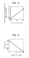
- FIG. 5 is a graph illustrating a relationship between the content of Ta of the insulating layer and a selection ratio of the insulating layer to the free layer;
- FIG. 6 is a graph illustrating a relationship between the content of Ta of the insulating layer and an MR ratio
- FIG. 7 is a schematic diagram of a magnetoresistive element illustrating a process flow of etching a free layer, in a method of manufacturing a magnetoresistive element according to a second embodiment of the present invention.
- FIG. 8 is a schematic diagram for describing an effect in the method of manufacturing a magnetoresistive element according to the second embodiment of the present invention.
- a first embodiment according to the present invention will be described with reference to FIG. 4 .
- FIG. 4 illustrates a schematic diagram after a free layer of a magnetoresistive element is etched by plasma etching, in a method for manufacturing a magnetoresistive element according to a first embodiment.
- reference numeral 201 represents a Si substrate
- reference numeral 202 represents an electrode film
- reference numeral 203 represents an underlayer for controlling crystallinity of a fixed layer or stabilizing a magnetization of the fixed layer
- reference numeral 204 represents a fixed layer
- reference numeral 401 represents (MgO) 100-x Ta x that is a Ta-containing insulating layer
- reference numeral 206 represents CoFeB that is a free layer
- reference numeral 207 represents a cap layer for protecting the free layer
- reference numeral 208 represents a hard mask, and each layer above the electrode film 202 is sequentially formed on the substrate 201 .
- the substrate on which each layer is formed may be prepared.
- the electrode film 202 a laminated film of a Ta film having a thickness of 5 nm and a Ru film having a thickness of 10 nm is used, as the underlayer 203 , a Ta layer having a thickness of 5 nm is used, as the fixed layer 204 , a CoFeB layer having a thickness of 5 nm is used, as the free layer 206 , a CoFeB layer having a thickness of 4 nm is used, as the cap layer 207 , a laminated film of a Ta layer having a thickness of 5 nm and a Ru layer having a thickness of 5 nm is used, and as the hard mask 208 , a Ta film having a thickness of 70 nm is used.
- the thickness of the Ta-containing insulating layer 401 is set to be 2.1 nm.
- the processes up to FIG. 4 are basically the same as those of FIG. 2 , but are different from those of FIG. 2 , in terms of compositions of the insulating layer 205 or a method for forming the insulating layer 205 .
- the magnetoresistive element is formed to have the structure illustrated in FIG. 4 and is then manufactured by processing layers under the insulating layer by the known method.
- transistors for selecting each resistive element or wirings for coupling each element are formed between the Si substrate 201 and the electrode film 202 .
- the underlayer 203 or the cap layer 207 is not present.
- the selection ratio of the insulating layer may be improved and characteristics that can be practically used as the magnetoresistive element may be shown, by inserting the Ta-containing insulating layer 401 between the fixed layer 204 and the free layer 206 . The reason will be described with reference to FIGS. 5 and 6 .
- FIG. 5 illustrates dependency of the content of Ta of the selection ratio of the insulating layer to the free layer when the CoFeB is used as the free layer and the Ta-containing insulating layer (MgO) 100-x Ta x in which MgO and Ta are mixed is used as the insulating layer.
- the content of Ta is represented by a volume ratio (vol %) and the selection ratio of the insulating layer is calculated from the results etched under the following etching condition 2 by using an ICP type of plasma source.
- the experiment is performed by setting a content ratio of Ta to be 0 vol % when only the MgO is used as the insulating layer, and the content ratio of Ta to be 100 vol % when only Ta is used as the insulating layer, such that the selection ratio of the insulating layer therebetween is calculated by collinear approximation.
- CO gas flow rate 10 ccm
- NH 3 gas flow rate 50 ccm
- process pressure 0.3 Pa
- source power 1200 W
- wafer bias power 300 W
- the selection ratio of the insulating layer represents a value larger than 80.
- the selection ratio of the insulating layer is 5.9 or more, but it can be appreciated from FIG. 5 that the selection ratio of the insulating layer can be achieved when the insulating layer contains Ta of 5.1 vol % or more.
- FIG. 6 illustrates dependency of the content of Ta of an MR ratio when the CoFeB is used as the free layer and the (MgO) 100-x Ta x in which MgO and Ta are mixed is used as the insulating layer.
- the content of Ta is represented by the volume ratio (vol %).
- the MR ratio having the content of Ta of 0 vol % the known 604% is used.
- the insulating layer is formed of only Ta representing conductive property, and thus loses the function as the insulating layer, such that the MR ratio is set to be 0%.
- the MR ratios having the content ratio of Ta of 0 vol % and the content ratio of Ta of 100 vol % are calculated by the collinear approximation.
- the selection ratio of the insulating layer that can manufacture the magnetoresistive element showing good characteristics on the entire surface of the wafer having a diameter of 300 mm achieves 5.9 or more and the MR ratio that can be practically used as the magnetoresistive element achieves 150% or more, by setting the content ratio of Ta to be ranging from 5.1 vol % and 75.2 vol % using the Ta-containing insulating layer (MgO) 100-x Ta x as the insulating layer.
- MgO Ta-containing insulating layer
- the mixed gas of the CO gas and the NH 3 gas that are mixed at a 1:5 ratio of NH 3 to CO is used, but in the present process, the etching rate of Ta is slower than that of CoFeB by using only the CO gas or only the NH 3 gas.
- the etching rate of Ta is slower than that of CoFeB by using the CH 3 OH gas.
- the controlled Ta may be used in the process using the mixed gas of the CO gas and the NH 3 gas of which the mixed ratio is changed or the CH 3 OH gas.
- the embodiment describes the CoFeB as the free layer and the material in which Ta is contained in MgO as the Ta-containing insulating layer, but it is possible to expect the same effect even when other magnetic materials such as NiFe are used as the free layer or even when Ta is contained in another insulating layer of AlO, MgAlO, and the like, instead of MgO. Further, it is possible to expect the same effect even when a Ta-containing material such as TaC, TaS, TaSi, TaN, TaO as well as Ta is mixed in the insulating layer.
- the material of the free layer, the material of the insulating layer, or the composition of the Ta-containing material is not particularly limited.
- the density of the Ta-containing material is greatly changed due to the oxidation, when the Ta-containing material is oxidized after the formation of the film, the density of the Ta-containing material is suddenly changed due to the oxidation process, such that cracks occur in the insulating layer and the magnetic characteristics greatly deteriorate. Therefore, when manufacturing a Ta-containing insulating layer, the entire surface of the film is oxidized after the formation of the film and then, the film such as the free layer must not be formed on the upper portion thereof.
- the Ta-containing insulating layer when the Ta-containing insulating layer is formed, it is preferable to form a film by sputtering a single target obtained by mixing MgO and a Ta-containing material, a single target obtained by mixing AlO and a Ta-containing material, or a single target obtained by mixing MgAlO and a Ta-containing material under the atmosphere of noble gases such as He, Ne, Ar, Kr, Xe, or the like.
- the Ta-containing insulating layer may be formed by simultaneously sputtering a plurality of targets by using MgO and a Ta-containing material, AlO and a Ta-containing material, or MgAlO and a Ta-containing material as a separate target.
- targets formed of C, Si, and the like may be used simultaneously.
- the Ta-containing material is oxidized after the formation of the film, cracks occur in the insulating layer due to the sudden change in density, but when the Ta-containing material is oxidized during the formation of the film, the density is slowly changed to suppress the occurrence of cracks.
- the Ta-containing insulating layer may be formed by sputtering the single target or the plurality of targets of Mg and a Ta-containing material, Al and a Ta-containing material, or MgAl and a Ta-containing material under the atmosphere in which oxygen is contained in the noble gases or the oxygen atmosphere. Further, in order to obtain the desired TaN-containing insulating layer, the TaN-containing insulating layer may be formed by performing the sputtering under the atmosphere in which nitrogen is contained in the noble gases or the nitrogen-containing atmosphere but the film forming atmosphere during the sputtering is not particularly limited.
- the process of using the mixed gas of the CO gas and the NH 3 gas as described above and the CH 3 OH gas reduces the etching rate of the Ti-containing materials such as Ti, TiN, TiAl, TiB, TiC, TiO, TiS, TiSi, and the like, than that of CoFeB. Therefore, when the selection ratio of the insulating layer meets 5.9 or more and the MR ratio meets 150% or more, the Ti-containing material may be used instead of the Ta-containing material.
- a method for forming a film by mixing Mg and a Ti-containing material or Al and a Ti-containing material, and oxidizing the entire surface of the formed film by a plasma oxidation method, an ozone oxidation method, or a radical oxidation method, and the like to manufacture the Ti-containing insulating layer, and then, forming a film, such as the free layer on the upper portion of the Ti-containing insulating layer may also be considered.
- the density of the Ti-containing material is greatly changed due to the oxidation, and thus when the Ti-containing material is oxidized after the formation of the film, the density of the Ta-containing material is suddenly changed due to the oxidation process, such that cracks occur in the insulating layer and the magnetic characteristics greatly deteriorate. Therefore, when manufacturing the Ti-containing insulating layer, the entire surface of the film is oxidized after the formation of the film and then, the film, such as the free layer must not be formed on the upper portion thereof.
- the Ti-containing insulating layer when the Ti-containing insulating layer is formed, it is preferable to form a film by sputtering a single target obtained by mixing MgO and a Ti-containing material, a single target obtained by mixing AlO and a Ti-containing material, or a single target obtained by mixing MgAlO and a Ti-containing material under the atmosphere of noble gases such as He, Ne, Ar, Kr, Xe, or the like.
- the Ti-containing insulating layer may be formed by simultaneously sputtering a plurality of targets by using MgO and a Ti-containing material, AlO and a Ti-containing material, or MgAlO and a Ti content material as a separate target.
- targets formed of C, Si, and the like may be used simultaneously.
- the Ti-containing material is oxidized after the formation of the film, cracks occur in the insulating layer due to the sudden change in density, but when the Ti-containing material is oxidized during the formation of the film, the density is slowly changed to suppress the occurrence of cracks.
- the Ti-containing insulating layer may be formed by sputtering the single target or the plurality of targets of Mg and a Ta-containing material, Al and a Ti-containing material, or MgAl and a Ti-containing material under the atmosphere in which oxygen is contained in the noble gases or the oxygen atmosphere.
- the TiN containing insulating layer may be formed by performing the sputtering under the atmosphere in which nitrogen is contained in the noble gases or the nitrogen-containing atmosphere, but the film forming atmosphere during the sputtering is not particularly limited.
- FIGS. 7 and 8 A second embodiment according to the present invention will be described with reference to FIGS. 7 and 8 . Further, the configurations that are described in the first embodiment but not described in this embodiment can be applied to this embodiment unless the circumstances are exceptional.
- FIG. 7 is a schematic diagram of a magnetoresistive element illustrating a process flow of etching a free layer by plasma etching, in a method of manufacturing a magnetoresistive element according to Embodiment 2.
- reference numeral 201 represents a Si substrate
- reference numeral 202 represents an electrode film
- reference numeral 203 represents an underlayer for controlling crystallinity of a fixed layer or stabilizing a magnetization of the fixed layer
- reference numeral 204 represents the fixed layer
- reference numeral 701 represents a first insulating layer
- reference numeral 702 represents an inter-layer Ta-containing layer
- reference numeral 703 represents a second insulating layer
- reference numeral 206 represents a free layer
- reference numeral 207 represents a cap layer for protecting the free layer
- reference numeral 208 represents a hard mask
- reference numeral 209 represents a resist mask, and each layer above the electrode film 202 is sequentially formed on the substrate 201 .
- the substrate on which each layer is formed may be prepared.
- transistors for selecting each resistive element or wirings for coupling each element are formed between the Si substrate 201 and the electrode film 202 .
- the underlayer 203 or the cap layer 207 is not present.
- each layer is formed, the hard mask layer 208 and the cap layer 207 are etched (FIG. 7 ( 1 )), and then only the free layer 206 is etched (FIG. 7 ( 2 )).
- the magnetoresistive element is formed to have the structure illustrated in the right drawing of FIG. 7 and is then manufactured by processing layers under the insulating layer by a known method.
- the plasma etching is promoted by applying the wafer bias power to the stage, on which the wafer is disposed, to positively attract ions in plasma to the wafer.
- the etching is performed on a etched surface, and at the same time, a plurality of ions are also attracted to the etched surface, and elements of a layer under the etched surface are diffused to an upper layer thereof by the attracted ions.
- the process having high ion energy is used during the process of etching the free layer 206 that is a magnetic material shown in FIG. 7 , such that the diffusion of elements are promoted. Therefore, in the process ( 2 ) shown in FIG.
- FIG. 8 schematically illustrates the state.
- a Ta-containing insulating layer 801 is formed on the processed surface by diffusing the inter-layer Ta-containing layer 702 to the second insulating layer 703 .
- the selection ratio of the insulating layer is increased when Ta is contained in the insulating layer, such that the selection ratio of the insulating layer is improved only on the processed surface by the formation of the Ta-containing insulating layer 801 .
- an amount of Ta diffused from the Ta-containing layer 702 is increased further at a thinner side of the second insulating layer, such that the selection ratio of the insulating layer is increased. Therefore, Even though the selection ratio of the insulating layer is insufficient in a part inside the wafer surface, and thus the etching of the second insulating layer is performed, the selection ratio of the insulating layer is increased according to the reduction in the film thickness and thus it is possible to achieve the selection ratio of the insulating layer of 5.9 or more during the etching of the second insulating layer.
- the magnetoresistive element showing the good characteristics on the entire surface of the wafer having a diameter of 300 mm by preventing the characteristics of the magnetoresistive element from deteriorating due to the penetration of a part of the insulating layer just under the free layer.
- the magnetoresistive element has a structure in which the Ta-containing layer 702 is interposed between the first insulating layer 701 and the second insulating layer 703 , but if not specifically required, the first insulating layer 701 may be removed. However, when not contacting the first insulating layer 701 , the magnetic characteristics of a pin layer (fixed layer) 204 are likely to deteriorate, such that it is preferable to insert the first insulating layer 701 . Further, in FIGS. 7 and 8 , one Ta-containing layer is inserted between two insulating layers, but when the Ta-containing layer is formed just under the insulating layer, the number of Ta-containing layers is not particularly limited.
- the total of film thickness of all the insulating layers and the Ta-containing layers is preferably set to a finite value less than 3 nm.
- the Ta-containing layer has an island shape, such that it is difficult to keep the Ta-containing layer as one film.
- the thickness of one Ta-containing layer is 0.1 nm or more.
- the Ta-containing layer may be formed by containing only Ta, but the composition thereof is not particularly limited if the Ta-containing layer is a mixed part containing a Ta element, such as TaC, TaS, TaSi, TaN, and TaO.
- the process of using the mixed gas of the CO gas and the NH 3 gas and the CH 3 OH gas as described above reduces the etching rate of the Ti-containing material such as Ti, TiN, TiAl, TiB, TiC, TiO, TiS, TiSi, and the like, than that of the free layer. Therefore, when the selection ratio of the insulating layer meets 5.9 or more and the MR ratio meets 150% or more, the Ti-containing material may be used instead of the Ta-containing material.
- a magnetoresistive element having a multi-layer film structure including a free layer that is a magnetic layer of which the magnetization direction can be inverted by external magnetic field or spin injection, a fixed layer that is a magnetic layer of which the magnetization direction is not inverted by external magnetic field or spin injection, and an insulating layer interposed between the free layer and the fixed layer, the insulating layer is configured as a Ta-containing insulating layer.
- the Ta-containing insulating layer is formed of the mixed material of MgO and Ta and a ratio of Ta occupied within the Ta-containing layer is ranging from 5.1 vol % to 75.2 vol %.
- a magnetoresistive element having a multi-layer film structure including a free layer that is a magnetic layer of which the magnetization direction can be inverted by external magnetic field or spin injection, a fixed layer that is a magnetic layer of which the magnetization direction is not inverted by external magnetic field or spin injection, and an insulating layer interposed between the free layer and the fixed layer, the insulating layer is configured as a Ti-containing insulating layer.
- the magnetoresistive element having a multi-layer film structure including a free layer that is a magnetic layer of which the magnetization direction can be inverted by external magnetic field or spin injection and a fixed layer that is a magnetic layer of which the magnetization direction is not inverted by external magnetic field or spin injection, a Ta-containing layer interposed between two insulating layers is inserted between the fixed layer and the free layer.
- the magnetoresistive element having a multi-layer film structure including a free layer that is a magnetic layer of which the magnetization direction can be inverted by external magnetic field or spin injection and a fixed layer that is a magnetic layer of which the magnetization direction is not inverted by external magnetic field or spin injection, a Ta layer interposed between two MgO layers is inserted between the fixed layer and the free layer.
- the magnetoresistive element having a multi-layer film structure including a free layer that is a magnetic layer of which the magnetization direction can be inverted by external magnetic field or spin injection and a fixed layer that is a magnetic layer of which the magnetization direction is not inverted by external magnetic field or spin injection, a Ti-containing layer interposed between two insulating layers is inserted between the fixed layer and the free layer.
- the free layer is processed by plasma etching using NH 3 gas, CO gas, a mixed gas of the NH 3 gas and the CO gas, or CH 3 OH gas.
- the magnetoresistive element which can increase the selection ratio of the insulating layer to the free layer and shows the good characteristics on the entire surface of the wafer when the free layer of the magnetoresistive element is etched, by using the Ta-containing layer containing Ta or the Ti-containing layer containing Ti as the insulating layer of the magnetoresistive element.
- the magnetoresistive element which can increase the selection ratio of the insulating layer to the free layer and shows the good characteristics on the entire surface of the wafer, by inserting the Ta-containing layer or the Ti-containing layer, which is interposed between the two insulating layers, between the fixed layer and the free layer.
- the present invention is not limited to the foregoing embodiments, but includes various modifications.
- the foregoing embodiments are described in detail for easily describing the present invention, and are not essentially limited as those including all components that are described above.
- some of the configurations of any embodiment can be substituted into configurations of other embodiments and configurations of other embodiments can be added to the configuration of any embodiment.
- other configurations can be added, deleted and substituted.
Landscapes
- Engineering & Computer Science (AREA)
- Chemical & Material Sciences (AREA)
- Physics & Mathematics (AREA)
- Manufacturing & Machinery (AREA)
- Crystallography & Structural Chemistry (AREA)
- Condensed Matter Physics & Semiconductors (AREA)
- Power Engineering (AREA)
- General Physics & Mathematics (AREA)
- Computer Hardware Design (AREA)
- Nanotechnology (AREA)
- Mechanical Engineering (AREA)
- Organic Chemistry (AREA)
- Metallurgy (AREA)
- Materials Engineering (AREA)
- Inorganic Chemistry (AREA)
- General Chemical & Material Sciences (AREA)
- Chemical Kinetics & Catalysis (AREA)
- Analytical Chemistry (AREA)
- Plasma & Fusion (AREA)
- Spectroscopy & Molecular Physics (AREA)
- Microelectronics & Electronic Packaging (AREA)
- Hall/Mr Elements (AREA)
- Mram Or Spin Memory Techniques (AREA)
Applications Claiming Priority (2)
| Application Number | Priority Date | Filing Date | Title |
|---|---|---|---|
| JP2012-239921 | 2012-10-31 | ||
| JP2012239921A JP2014090109A (ja) | 2012-10-31 | 2012-10-31 | 磁気抵抗素子の製造方法 |
Publications (2)
| Publication Number | Publication Date |
|---|---|
| US20140116985A1 US20140116985A1 (en) | 2014-05-01 |
| US9097754B2 true US9097754B2 (en) | 2015-08-04 |
Family
ID=50546038
Family Applications (1)
| Application Number | Title | Priority Date | Filing Date |
|---|---|---|---|
| US13/748,665 Active 2033-02-20 US9097754B2 (en) | 2012-10-31 | 2013-01-24 | Method of manufacturing magnetoresistive element |
Country Status (4)
| Country | Link |
|---|---|
| US (1) | US9097754B2 (zh) |
| JP (1) | JP2014090109A (zh) |
| KR (2) | KR20140055908A (zh) |
| TW (1) | TWI508337B (zh) |
Cited By (1)
| Publication number | Priority date | Publication date | Assignee | Title |
|---|---|---|---|---|
| US11535930B2 (en) | 2019-09-16 | 2022-12-27 | Samsung Electronics Co., Ltd. | Sputtering apparatus and method of fabricating magnetic memory device using the same |
Families Citing this family (3)
| Publication number | Priority date | Publication date | Assignee | Title |
|---|---|---|---|---|
| US9099643B2 (en) * | 2013-02-26 | 2015-08-04 | Tdk Corporation | Method of etching a magnesium oxide film |
| KR102175471B1 (ko) | 2014-04-04 | 2020-11-06 | 삼성전자주식회사 | 자기 저항 메모리 장치 및 그 제조 방법 |
| WO2017151735A1 (en) * | 2016-03-01 | 2017-09-08 | Virginia Commonwealth University | Switching skyrmions with vcma/electric field for memory, computing, and information processing |
Citations (9)
| Publication number | Priority date | Publication date | Assignee | Title |
|---|---|---|---|---|
| JPH04111274A (ja) | 1990-08-31 | 1992-04-13 | Nec Ibaraki Ltd | 磁気ヘッド装置 |
| JPH08253881A (ja) * | 1995-03-15 | 1996-10-01 | Natl Res Inst For Metals | ドライエッチング方法 |
| US6936903B2 (en) | 2001-09-25 | 2005-08-30 | Hewlett-Packard Development Company, L.P. | Magnetic memory cell having a soft reference layer |
| US6947316B2 (en) * | 2000-07-06 | 2005-09-20 | Hitachi, Ltd. | Magnetoresistive sensor including magnetic domain control layers having high electric resistivity, magnetic head and magnetic disk apparatus |
| US20080112093A1 (en) | 2006-11-14 | 2008-05-15 | Fujitsu Limited | Tunneling magnetoresistance (TMR) device, its manufacture method, magnetic head and magnetic memory using TMR device |
| JP4111274B2 (ja) | 2003-07-24 | 2008-07-02 | キヤノンアネルバ株式会社 | 磁性材料のドライエッチング方法 |
| US20080164548A1 (en) | 2006-02-25 | 2008-07-10 | Yadav Technology | Low resistance high-tmr magnetic tunnel junction and process for fabrication thereof |
| US7576956B2 (en) | 2004-07-26 | 2009-08-18 | Grandis Inc. | Magnetic tunnel junction having diffusion stop layer |
| US8374025B1 (en) * | 2007-02-12 | 2013-02-12 | Avalanche Technology, Inc. | Spin-transfer torque magnetic random access memory (STTMRAM) with laminated free layer |
Family Cites Families (9)
| Publication number | Priority date | Publication date | Assignee | Title |
|---|---|---|---|---|
| JP2002314164A (ja) * | 2001-02-06 | 2002-10-25 | Sony Corp | 磁気トンネル素子及びその製造方法、薄膜磁気ヘッド、磁気メモリ、並びに磁気センサ |
| JP2004214459A (ja) * | 2003-01-06 | 2004-07-29 | Sony Corp | 不揮発性磁気メモリ装置及びその製造方法 |
| US7199055B2 (en) * | 2003-03-03 | 2007-04-03 | Cypress Semiconductor Corp. | Magnetic memory cell junction and method for forming a magnetic memory cell junction |
| JP4292128B2 (ja) * | 2004-09-07 | 2009-07-08 | キヤノンアネルバ株式会社 | 磁気抵抗効果素子の製造方法 |
| FR2892231B1 (fr) * | 2005-10-14 | 2008-06-27 | Commissariat Energie Atomique | Dispositif magnetique a jonction tunnel magnetoresistive et memoire magnetique a acces aleatoire |
| US8084835B2 (en) * | 2006-10-20 | 2011-12-27 | Avalanche Technology, Inc. | Non-uniform switching based non-volatile magnetic based memory |
| JP2011054873A (ja) * | 2009-09-04 | 2011-03-17 | Sony Corp | 不揮発性メモリ素子の製造方法 |
| US8558331B2 (en) | 2009-12-08 | 2013-10-15 | Qualcomm Incorporated | Magnetic tunnel junction device |
| JP5786341B2 (ja) * | 2010-09-06 | 2015-09-30 | ソニー株式会社 | 記憶素子、メモリ装置 |
-
2012
- 2012-10-31 JP JP2012239921A patent/JP2014090109A/ja active Pending
- 2012-12-18 TW TW101148067A patent/TWI508337B/zh active
-
2013
- 2013-01-23 KR KR1020130007284A patent/KR20140055908A/ko active Application Filing
- 2013-01-24 US US13/748,665 patent/US9097754B2/en active Active
-
2015
- 2015-10-16 KR KR1020150144559A patent/KR101813603B1/ko active IP Right Grant
Patent Citations (10)
| Publication number | Priority date | Publication date | Assignee | Title |
|---|---|---|---|---|
| JPH04111274A (ja) | 1990-08-31 | 1992-04-13 | Nec Ibaraki Ltd | 磁気ヘッド装置 |
| JPH08253881A (ja) * | 1995-03-15 | 1996-10-01 | Natl Res Inst For Metals | ドライエッチング方法 |
| JP2677321B2 (ja) | 1995-03-15 | 1997-11-17 | 科学技術庁金属材料技術研究所長 | ドライエッチング方法 |
| US6947316B2 (en) * | 2000-07-06 | 2005-09-20 | Hitachi, Ltd. | Magnetoresistive sensor including magnetic domain control layers having high electric resistivity, magnetic head and magnetic disk apparatus |
| US6936903B2 (en) | 2001-09-25 | 2005-08-30 | Hewlett-Packard Development Company, L.P. | Magnetic memory cell having a soft reference layer |
| JP4111274B2 (ja) | 2003-07-24 | 2008-07-02 | キヤノンアネルバ株式会社 | 磁性材料のドライエッチング方法 |
| US7576956B2 (en) | 2004-07-26 | 2009-08-18 | Grandis Inc. | Magnetic tunnel junction having diffusion stop layer |
| US20080164548A1 (en) | 2006-02-25 | 2008-07-10 | Yadav Technology | Low resistance high-tmr magnetic tunnel junction and process for fabrication thereof |
| US20080112093A1 (en) | 2006-11-14 | 2008-05-15 | Fujitsu Limited | Tunneling magnetoresistance (TMR) device, its manufacture method, magnetic head and magnetic memory using TMR device |
| US8374025B1 (en) * | 2007-02-12 | 2013-02-12 | Avalanche Technology, Inc. | Spin-transfer torque magnetic random access memory (STTMRAM) with laminated free layer |
Non-Patent Citations (3)
| Title |
|---|
| Keizo Kinoshita et al., Etching Magnetic Tunnel Junction with Metal Etchers, Japanese Journal of Applied Physics 49 (2010) 08JB02. |
| Office Action mailed Nov. 28, 2014 in Korean Patent Application No. 10-2013-0007284. |
| S. Ikeda et al., Tunnel magnetoresistance of 604% at 300K by suppression of Ta diffusion in CoFeB/MgO/CoFeB pseudo-spin-vales annealed at high temperature, Appli. Phys. Lett. 93, 082508 (2008). |
Cited By (2)
| Publication number | Priority date | Publication date | Assignee | Title |
|---|---|---|---|---|
| US11535930B2 (en) | 2019-09-16 | 2022-12-27 | Samsung Electronics Co., Ltd. | Sputtering apparatus and method of fabricating magnetic memory device using the same |
| US11834738B2 (en) | 2019-09-16 | 2023-12-05 | Samsung Electronics Co., Ltd. | Sputtering apparatus and method of fabricating magnetic memory device using the same |
Also Published As
| Publication number | Publication date |
|---|---|
| KR20150123211A (ko) | 2015-11-03 |
| KR20140055908A (ko) | 2014-05-09 |
| JP2014090109A (ja) | 2014-05-15 |
| US20140116985A1 (en) | 2014-05-01 |
| TWI508337B (zh) | 2015-11-11 |
| KR101813603B1 (ko) | 2017-12-29 |
| TW201417361A (zh) | 2014-05-01 |
Similar Documents
| Publication | Publication Date | Title |
|---|---|---|
| US7808026B2 (en) | Dry etching method and production method of magnetic memory device | |
| US20050048675A1 (en) | Method of etching magnetic material, magnetoresistive film and magnetic random access memory | |
| TWI730462B (zh) | 半導體裝置及其製造方法 | |
| JP5774568B2 (ja) | 半導体装置の製造方法 | |
| US7061034B2 (en) | Magnetic random access memory including middle oxide layer and method of manufacturing the same | |
| US9097754B2 (en) | Method of manufacturing magnetoresistive element | |
| US20070041125A1 (en) | Magnetic tunnel junction structure having an oxidized buffer layer and method of fabricating the same | |
| US11770977B2 (en) | Semiconductor structure and method for forming the same | |
| US20230296701A1 (en) | Magnetic Tunnel Junction Devices | |
| US8956882B1 (en) | Method of manufacturing magnetoresistive element | |
| JP5720681B2 (ja) | 薄膜磁気デバイス及びその製造方法 | |
| JP2006161120A (ja) | ホイスラー合金膜の成膜方法及びトンネル磁気抵抗素子 | |
| JP6616803B2 (ja) | 磁気抵抗素子の製造方法、及び磁気抵抗素子 | |
| KR20170019035A (ko) | 루테늄 박막의 식각방법 | |
| US20150069549A1 (en) | Magnetic element and method of manufacturing the same | |
| US20230138005A1 (en) | Magnetoresistive Random-Access Memory (MRAM) Structure For Improving Process Control And Method Of Fabricating Thereof | |
| CN112864315B (zh) | Mtj器件的制作方法 | |
| US20230263069A1 (en) | Memory device and manufacturing method thereof | |
| KR101588607B1 (ko) | 호이슬러 합금의 식각방법 |
Legal Events
| Date | Code | Title | Description |
|---|---|---|---|
| AS | Assignment |
Owner name: HITACHI HIGH-TECHNOLOGIES CORPORATION, JAPAN Free format text: ASSIGNMENT OF ASSIGNORS INTEREST;ASSIGNORS:SATAKE, MAKOTO;HAYAKAWA, JUN;TETSUKA, TSUTOMU;AND OTHERS;SIGNING DATES FROM 20121212 TO 20121220;REEL/FRAME:029684/0317 |
|
| STCF | Information on status: patent grant |
Free format text: PATENTED CASE |
|
| MAFP | Maintenance fee payment |
Free format text: PAYMENT OF MAINTENANCE FEE, 4TH YEAR, LARGE ENTITY (ORIGINAL EVENT CODE: M1551); ENTITY STATUS OF PATENT OWNER: LARGE ENTITY Year of fee payment: 4 |
|
| AS | Assignment |
Owner name: HITACHI HIGH-TECH CORPORATION, JAPAN Free format text: CHANGE OF NAME AND ADDRESS;ASSIGNOR:HITACHI HIGH-TECHNOLOGIES CORPORATION;REEL/FRAME:052259/0227 Effective date: 20200212 |
|
| MAFP | Maintenance fee payment |
Free format text: PAYMENT OF MAINTENANCE FEE, 8TH YEAR, LARGE ENTITY (ORIGINAL EVENT CODE: M1552); ENTITY STATUS OF PATENT OWNER: LARGE ENTITY Year of fee payment: 8 |