US8994432B2 - Semiconductor integrated circuit and method of operating the same - Google Patents
Semiconductor integrated circuit and method of operating the same Download PDFInfo
- Publication number
- US8994432B2 US8994432B2 US13/974,763 US201313974763A US8994432B2 US 8994432 B2 US8994432 B2 US 8994432B2 US 201313974763 A US201313974763 A US 201313974763A US 8994432 B2 US8994432 B2 US 8994432B2
- Authority
- US
- United States
- Prior art keywords
- clock
- output
- network
- clock signals
- semiconductor integrated
- Prior art date
- Legal status (The legal status is an assumption and is not a legal conclusion. Google has not performed a legal analysis and makes no representation as to the accuracy of the status listed.)
- Active
Links
- 239000004065 semiconductor Substances 0.000 title claims abstract description 63
- 238000000034 method Methods 0.000 title claims abstract description 14
- 230000004044 response Effects 0.000 claims description 6
- 238000010586 diagram Methods 0.000 description 12
- 230000003247 decreasing effect Effects 0.000 description 3
- 230000009977 dual effect Effects 0.000 description 3
- 230000007423 decrease Effects 0.000 description 2
- 230000006870 function Effects 0.000 description 2
- 230000008569 process Effects 0.000 description 2
- 238000013459 approach Methods 0.000 description 1
- 238000010420 art technique Methods 0.000 description 1
- 230000005540 biological transmission Effects 0.000 description 1
- 239000007795 chemical reaction product Substances 0.000 description 1
- 230000009467 reduction Effects 0.000 description 1
Images


Classifications
-
- G—PHYSICS
- G06—COMPUTING; CALCULATING OR COUNTING
- G06F—ELECTRIC DIGITAL DATA PROCESSING
- G06F1/00—Details not covered by groups G06F3/00 - G06F13/00 and G06F21/00
- G06F1/04—Generating or distributing clock signals or signals derived directly therefrom
- G06F1/10—Distribution of clock signals, e.g. skew
-
- G—PHYSICS
- G06—COMPUTING; CALCULATING OR COUNTING
- G06F—ELECTRIC DIGITAL DATA PROCESSING
- G06F1/00—Details not covered by groups G06F3/00 - G06F13/00 and G06F21/00
- G06F1/26—Power supply means, e.g. regulation thereof
- G06F1/32—Means for saving power
- G06F1/3203—Power management, i.e. event-based initiation of a power-saving mode
- G06F1/3234—Power saving characterised by the action undertaken
- G06F1/324—Power saving characterised by the action undertaken by lowering clock frequency
-
- G—PHYSICS
- G06—COMPUTING; CALCULATING OR COUNTING
- G06F—ELECTRIC DIGITAL DATA PROCESSING
- G06F1/00—Details not covered by groups G06F3/00 - G06F13/00 and G06F21/00
- G06F1/26—Power supply means, e.g. regulation thereof
- G06F1/32—Means for saving power
-
- H—ELECTRICITY
- H03—ELECTRONIC CIRCUITRY
- H03L—AUTOMATIC CONTROL, STARTING, SYNCHRONISATION OR STABILISATION OF GENERATORS OF ELECTRONIC OSCILLATIONS OR PULSES
- H03L7/00—Automatic control of frequency or phase; Synchronisation
-
- Y—GENERAL TAGGING OF NEW TECHNOLOGICAL DEVELOPMENTS; GENERAL TAGGING OF CROSS-SECTIONAL TECHNOLOGIES SPANNING OVER SEVERAL SECTIONS OF THE IPC; TECHNICAL SUBJECTS COVERED BY FORMER USPC CROSS-REFERENCE ART COLLECTIONS [XRACs] AND DIGESTS
- Y02—TECHNOLOGIES OR APPLICATIONS FOR MITIGATION OR ADAPTATION AGAINST CLIMATE CHANGE
- Y02D—CLIMATE CHANGE MITIGATION TECHNOLOGIES IN INFORMATION AND COMMUNICATION TECHNOLOGIES [ICT], I.E. INFORMATION AND COMMUNICATION TECHNOLOGIES AIMING AT THE REDUCTION OF THEIR OWN ENERGY USE
- Y02D10/00—Energy efficient computing, e.g. low power processors, power management or thermal management
Definitions
- Exemplary embodiments relate to a semiconductor integrated circuit. More particularly, exemplary embodiments relate to a semiconductor integrated circuit which reduces power consumption by having a new clock path for transmission of a clock signal, and a method of operating the same.
- the portable devices of the related art may include many synchronization circuits which operate in synchronization with a clock signal.
- dynamic voltage and frequency scaling DVFS
- DVFS is a method for reducing power consumed by synchronization circuits.
- DVFS is a power-saving technique used in various types of synchronization circuits.
- DVFS is a related art technique that increases the voltage and frequency of a portable device when the portable device shows the maximum performance. Further, DVFS in the related art decreases the frequency according to necessary performance for an application of the portable device, and decreases the voltage to a level that can be driven at the decreased frequency, when the maximum performance is not needed. Thus, the power consumption of the portable device in the related art is reduced. According to DVFS in the related art, decreasing the voltage exerts more influence on the reduction of power consumption than decreasing the frequency.
- semiconductor integrated circuits are designed to satisfy maximum performance. As a result, when the portable device of the related art does not require the maximum performance, a clock network for high-end products designed for the maximum performance will require greater power consumption than the performance needs.
- a method of operating a semiconductor integrated circuit may be provided.
- the method may include dividing a clock signal into first output clock signals with a high frequency, dividing the clock signal into second output clock signal with a non-high frequency, and selecting and sinking one of the first output clock signals and the second output clock signals, according to a power mode.
- the first output clock signals may be generated by driving the clock signal to a first clock network configured in mesh structure.
- the second output clock signals may be generated by driving the clock signal to a second clock network configured in mesh structure with less density than the mesh structure of the first clock network.
- the power mode may include a maximum performance mode and a non-maximum performance mode.
- the first output clock signals may be selected and sunk in the maximum performance mode and the second output clock signals may be selected and sunk in the non-maximum performance mode.
- a semiconductor integrated circuit including a first clock network configured to divide a clock signal into first output clock signals with a high frequency, a second clock network configured to divide the clock signal into second output clock signal with a non-high frequency, a plurality of selection circuits configured to be connected between the first clock network and the second clock network, and configured to select and output one of the first output clock signals and the second output clock signals, according to a power mode, and a plurality of clock sinks configured to sink output clock signals respectively output from the selection circuits.
- the first clock network may be configured in a mesh structure
- the second clock network may be configured in mesh structure with less density than the mesh structure of the first clock network
- the first clock network may be configured in a mesh structure
- the second clock network may be configured in a tree structure with less density than the mesh structure of the first clock network
- Each of the selection circuits maybe a NOR gate circuit configured to receive one of the first output clock signals and one of the second output clock signals, and one of the first clock network and the second clock network, which is not selected according to the power mode, may be fixed to a ground voltage.
- each of the selection circuits may be a NAND gate circuit configured to receive one of the first output clock signals and one of the second output clock signals, and one of the first clock network and the second clock network, which is not selected according to the power mode, may be fixed to a supply voltage.
- Each of the clock sinks may be a flip-flop configured to output a data signal in response to the respective output clock signal output from a respective selection circuit.
- the semiconductor integrated circuit may further include a power mode detector configured to monitor the power mode of the semiconductor integrated circuit, and configured to output a selection signal.
- each of the selection circuits may be a multiplexer configured to output one of the first output clock signals and the second output clock signals, according to the selection signal.
- the first clock network and the second clock network may be positioned on different layers, or on a same layer.
- the selection circuits may select the first clock network when the power mode is a maximum performance mode, and select the second clock network when the power mode is a non-maximum performance mode.
- a semiconductor integrated circuit including a first clock network configured in a mesh structure to generate first output clock signals, a second clock network configured in a tree structure to generate second output clock signals, a plurality of selection circuits configured to receive the first output clock signals and the second output clock signals, each of the selection circuits is configured to select and output one of the first output clock signals or one of the second output clock signals, according to a power mode; and a plurality of clock sinks configured to receive the one of the first output clock signals or one of the second output clock signals from respective selection circuits, each of the clock sinks is configured to sink the one of the first output clock signals or one of the second output signals output from a respective selection circuit.
- the plurality of selection circuits are further configured to be connected between the first clock network and the second clock network.
- FIG. 1 is a block diagram of a semiconductor integrated circuit including a clock network according to some embodiments
- FIG. 2 is a diagram of the clock network illustrated in FIG. 1 , which has mesh-mesh topology, according to some embodiments;
- FIG. 3 is a diagram of the clock network illustrated in FIG. 1 , which has mesh-tree topology, according to other embodiments
- FIG. 4 is a schematic block diagram of a data processing device including the semiconductor integrated circuit illustrated in FIG. 1 according to some embodiments;
- FIG. 5 is a schematic block diagram of a data processing device including the semiconductor integrated circuit illustrated in FIG. 1 according to other embodiments;
- FIG. 6 is a schematic block diagram of a data processing device including the semiconductor integrated circuit illustrated in FIG. 1 according to further embodiments.
- FIG. 7 is a graph showing the comparison of power consumption among semiconductor integrated circuits using the clock network illustrated in FIG. 1 .
- first, second, etc. may be used herein to describe various elements, these elements should not be limited by these terms. These terms are only used to distinguish one element from another. For example, a first signal could be termed a second signal, and, similarly, a second signal could be termed a first signal without departing from the teachings of the disclosure.
- FIG. 1 is a block diagram of a semiconductor integrated circuit 1 including a clock network according to some embodiments.
- the semiconductor integrated circuit 1 includes a high-end clock network 100 , a non-high-end clock network 200 , a plurality of selection circuits 10 , and a plurality of clock sinks 20 .
- a clock signal CLK which has been output and buffered by a clock source, e.g., a phase locked loop (PLL) or a delay locked loop (DLL), is input to the semiconductor integrated circuit 1 , i.e., the high-end clock network 100 and the non-high-end clock network 200 .
- a clock source e.g., a phase locked loop (PLL) or a delay locked loop (DLL)
- the high-end clock network 100 may divide the clock signal CLK into first output clock signals COUT 1 with a high frequency.
- the high-end clock network 100 transmits the clock signal CLK to a plurality of branches.
- the high-end clock network 100 may be referred to as a first clock network.
- the high-end clock network 100 may be implemented as a clock tree, including a plurality of tree branches. Each tree branch is a clock path through which the clock signal CLK is transmitted to a destination, i.e., an intellectual property (IP) connected to an end of the branch.
- IP intellectual property
- the selection circuits 10 may be connected with the tree branches, respectively.
- the high-end clock network 100 may be implemented in a mesh structure, i.e., it may have a plurality of mesh branches.
- the selection circuits 10 may be respectively connected with the mesh branches, which transmit the clock signal CLK.
- the non-high-end clock network 200 may divide the clock signal CLK into second output clock signals COUT 2 with a non-high frequency.
- the non-high-end clock network 200 may be referred to as a second clock network since it divides the clock signal CLK into signals with a low frequency or a medium frequency.
- the non-high-end clock network 200 may be implemented as a clock tree, including a plurality of tree branches. Each tree branch is a clock path through which the clock signal CLK is transmitted to a destination, i.e., an IP connected to an end of the branch.
- the selection circuits 10 may be connected with the tree branches, respectively.
- the non-high-end clock network 200 may be implemented in a mesh structure, i.e., it may have a plurality of mesh branches.
- the selection circuits 10 may be connected with the mesh branches, respectively, which transmit the clock signal CLK.
- the high-end clock network 100 and the non-high-end clock network 200 may be positioned on the same layer or different layers, respectively.
- the selection circuits 10 are connected between the high-end clock network 100 and the non-high-end clock network 200 . Each of the selection circuits 10 selects and outputs either a first output clock signal COUT 1 or a second output clock signal COUT 2 , according to a power mode of the semiconductor integrated circuit 1 . Each of the selection circuits 10 may be implemented as a logic circuit, which selects either of the first and second output clock signals COUT 1 and COUT 2 .
- the logic circuit may be a multiplexer, a NAND circuit, or a NOR circuit.
- the power mode includes a maximum performance mode and a non-maximum performance mode.
- the selection circuits 10 may select the maximum performance mode for an application expected to consume a lot of power for applications executed in the semiconductor integrated circuit 1 , and output the first output clock signal COUT 1 .
- the selection circuit 10 may select the non-maximum performance mode, and output the second output clock signal COUT 2 .
- the clock sinks 20 are respectively connected with the selection circuits 10 . Each of the clock sinks 20 generate and sink a pulse using an output clock signal COUT, selected and output by a corresponding selection circuit 10 .
- the output clock signal COUT which has been sunk, is transmitted to other elements (e.g., IPs) of the semiconductor integrated circuit 1 .
- the clock sink 20 may be implemented as a sequential logic circuit, which operates in response to the output clock signal COUT.
- the sequential logic circuit may be implemented by a register, a latch, or a flip-flop.
- the semiconductor integrated circuit 1 may also include a power mode detector (not shown), which monitors the power mode of the semiconductor integrated circuit 1 and outputs a selection signal.
- Each of the selection circuits 10 may be implemented as a multiplexer, which outputs one of the first and second output clock signals COUT 1 and COUT 2 in response to the selection signal output from the power mode detector.
- FIG. 2 is a diagram of the clock network illustrated in FIG. 1 , which has mesh-mesh topology, according to some embodiments.
- the high-end clock network 100 illustrated in FIG. 1 may be implemented by a high-end clock network 110 in a mesh structure in a semiconductor integrated circuit 2 , as shown in FIG. 2 .
- the high-end clock network 110 implemented in the mesh structure receives and divides the clock signal CLK into the first output clock signals COUT 1 , and the first output clock signals COUT 1 are respectively output through selection circuits 11 to the clock sinks 20 , respectively.
- the non-high-end clock network 200 illustrated in FIG. 1 may be implemented by a non-high-end clock network 210 in a mesh structure shown in the semiconductor integrated circuit 2 illustrated in FIG. 2 .
- the non-high-end clock network 210 implemented in the mesh structure receives and divides the clock signal CLK into the second output clock signals COUT 2 and the second output clock signals COUT 2 are output through selection circuits 11 , respectively, to the clock sinks 20 , respectively.
- the non-high-end clock network 210 has a lower density than the high-end clock network 110 .
- the mesh structure of the non-high-end clock network 210 is less dense than that of the high-end clock network 110 . Therefore, a second output clock signal COUT 2 , with a lower frequency (a low or medium frequency), than a first output clock signal COUT 1 , with a high frequency, is generated from each of the branches of the non-high-end clock network 210 .
- Each of the selection circuits 11 is connected between a branch of the high-end clock network 110 and a branch of the non-high-end clock network 210 , and outputs either the first output clock signal COUT 1 or the second output clock signal COUT 2 .
- each selection circuit 11 is implemented by a NAND circuit
- the high-end clock network 110 or the non-high-end clock network 210 which is not selected, is fixed to a supply voltage.
- each selection circuit 11 is implemented by a NOR circuit
- the high-end clock network 110 or the non-high end clock network 210 which is not selected, is fixed to a ground voltage.
- one of the clock sinks 20 is connected to each of the selection circuits 11 to sink the selected output clock signal COUT 1 or COUT 2 .
- FIG. 3 is a diagram of the clock network illustrated in FIG. 1 , which has mesh-tree topology, according to other embodiments.
- the high-end clock network 100 illustrated in FIG. 1 may be implemented by a high-end clock network 120 in a mesh structure in a semiconductor integrated circuit 3 , as shown in FIG. 3 .
- the non-high-end clock network 200 illustrated in FIG. 1 may be implemented by a non-high-end clock network 220 in a tree structure in the semiconductor integrated circuit 3 , as shown in FIG. 3 .
- the non-high-end clock network 220 implemented in the tree structure including a plurality of tree branches, receives and divides the clock signal CLK into the second output clock signals COUT 2 , and the second output clock signals COUT 2 are respectively output through selection circuits 12 , to the clock sinks 20 , respectively.
- the non-high-end clock network 220 has a lower density than the high-end clock network 120 .
- Each branch of the non-high-end clock network 220 generates a second output clock signal COUT 2 , with a lower frequency (a low or medium frequency) than a first output clock signal COUT 1 , with a high frequency.
- Each of the selection circuits 12 is connected between a branch of the high-end clock network 120 and a branch of the non-high-end clock network 220 and outputs either the first output clock signal COUT 1 or the second output clock signal COUT 2 .
- the clock network 120 or 220 which is not selected, is fixed to a supply voltage.
- the clock network 120 or 220 which is not selected, is fixed to a ground voltage.
- one of the clock sinks 20 is connected to each of the selection circuits 12 to sink the selected output clock signal COUT 1 or COUT 2 .
- FIG. 4 is a schematic block diagram of a data processing device 300 , including the semiconductor integrated circuit (IC) 1 illustrated in FIG. 1 , according to some embodiments.
- the data processing device 300 includes the semiconductor IC 1 , a data source 310 , and a clock source 320 .
- the data processing device 300 may be any device including a sequential logic circuit that can process data DATA output from the data source 310 , in response to the clock signal CLK.
- the data processing device 300 may be a system on chip (SOC), a processor, a central processing unit (CPU), a personal computer (PC), a data server, or a portable device.
- SOC system on chip
- CPU central processing unit
- PC personal computer
- data server or a portable device.
- the portable device may be implemented by a handheld device, such as a laptop computer, a mobile phone, smart phone, a tablet PC, a personal digital assistant (PDA), an enterprise digital assistant (EDA), a digital still camera, a digital video camera, a portable multimedia player (PMP), a personal navigation device or portable navigation device (PND), a car navigation system, a handheld game console, or an e-book.
- a handheld device such as a laptop computer, a mobile phone, smart phone, a tablet PC, a personal digital assistant (PDA), an enterprise digital assistant (EDA), a digital still camera, a digital video camera, a portable multimedia player (PMP), a personal navigation device or portable navigation device (PND), a car navigation system, a handheld game console, or an e-book.
- the semiconductor IC 1 sends the clock signal CLK output from the clock source 320 , or a clock signal buffered by a buffer, to tree branches of the clock networks 100 and 200 .
- the clock signal CLK may be divided into the first output clock signals COUT 1 with a high frequency.
- the first output clock signals COUT 1 may be generated by driving the clock signal CLK to the high-end clock network 100 .
- the clock signal CLK may also be divided into the second output clock signals COUT 2 with a non-high frequency (a low or medium frequency).
- the second output clock signals COUT 2 may be generated by driving the clock signal to the non-high-end clock network 200 .
- the first and second clock networks 100 and 200 include a plurality of branches, which may be implemented in a mesh or tree structure.
- the non-high-end clock network 200 is implemented such that the non-high-end clock network 200 has less density than the high-end clock network 100 . Therefore, the second output clock signals COUT 2 have a lower frequency than the first output clock signals COUT 1 .
- the semiconductor IC 1 selects one of output clock signals COUT, i.e., a first output clock signal COUT 1 and a second output clock signal COUT 2 output from respective tree branches, and sinks the selected output clock signal COUT 1 or COUT 2 according to a power mode.
- the first output clock signal COUT 1 may be selected and sunk.
- the second output clock signal COUT 2 may be selected, and sunk.
- the semiconductor IC 1 processes the data DATA output from the data source 310 in response to the output clock signal COUT 1 or COUT 2 , which has been sunk, and outputs processed data PDATA.
- At least one of the clock networks 100 and 200 may be implemented in a tree or mesh structure.
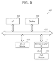
- FIG. 5 is a schematic block diagram of a data processing device 400 including the semiconductor IC 1 illustrated in FIG. 1 , according to other embodiments.
- the data processing device 400 includes the semiconductor IC 1 , a microprocessor 420 , a display 430 , and a data source 450 , which communicate with each another through a bus 410 .
- the data source 450 may be an embedded memory, or an external memory.
- the data processing device 400 also includes a clock source 440 generating a clock signal CLK.
- the data processing device 400 may be implemented as a PC, a data server, or a portable device.
- the clock source 440 performs the same function as the clock source 320 , illustrated in FIG. 4 .
- the data source 450 performs the same function as the data source 310 , illustrated in FIG. 4 .
- clock networks implemented in the semiconductor IC 1 are selectively used, according to the expected power consumption of an application. Therefore, power consumption of the semiconductor IC 1 can be significantly reduced.
- FIG. 6 is a schematic block diagram of a data processing device 500 , including the semiconductor IC 1 illustrated in FIG. 1 , according to further embodiments.
- the data processing device 500 may be implemented as a single IC, or a single SOC.
- the data processing device 500 includes the semiconductor IC 1 and a logic circuit 510 .
- the logic circuit 510 may be implemented by volatile or non-volatile memory.
- a clock sink implemented in the semiconductor IC 1 , may communicate data with the logic circuit 510 .
- input data Data-In is processed by the semiconductor IC 1 and the logic circuit 510 , and then output as output data Data-Out.
- FIG. 7 is a graph showing a comparison of power consumption among semiconductor ICs, using the clock network illustrated in FIG. 1 .
- the power consumption is different, depending on the embodiments of the clock network.
- power consumption is reduced when a dual clock network (e.g., a dual mesh structure or a dual mesh-tree structure) including different clock networks selectively used according to a power mode is used, as compared to when a single high-end clock network (e.g., a mesh structure or a tree structure) is used, regardless of the power mode.
- a dual clock network e.g., a dual mesh structure or a dual mesh-tree structure
- a single high-end clock network e.g., a mesh structure or a tree structure
- a different clock network is used, according to a power mode of a semiconductor IC. Therefore, the power consumption of the semiconductor IC is reduced. Since the power consumption of the semiconductor IC is reduced, power consumed in a data processing device, including the semiconductor IC, is also reduced.
Landscapes
- Engineering & Computer Science (AREA)
- Theoretical Computer Science (AREA)
- Physics & Mathematics (AREA)
- General Engineering & Computer Science (AREA)
- General Physics & Mathematics (AREA)
- Semiconductor Integrated Circuits (AREA)
- Design And Manufacture Of Integrated Circuits (AREA)
- Nonlinear Science (AREA)
Applications Claiming Priority (2)
| Application Number | Priority Date | Filing Date | Title |
|---|---|---|---|
| KR10-2012-0138048 | 2012-11-30 | ||
| KR1020120138048A KR102012904B1 (ko) | 2012-11-30 | 2012-11-30 | 반도체 집적회로와 그 동작 방법 |
Publications (2)
| Publication Number | Publication Date |
|---|---|
| US20140152372A1 US20140152372A1 (en) | 2014-06-05 |
| US8994432B2 true US8994432B2 (en) | 2015-03-31 |
Family
ID=50824848
Family Applications (1)
| Application Number | Title | Priority Date | Filing Date |
|---|---|---|---|
| US13/974,763 Active US8994432B2 (en) | 2012-11-30 | 2013-08-23 | Semiconductor integrated circuit and method of operating the same |
Country Status (2)
| Country | Link |
|---|---|
| US (1) | US8994432B2 (ko) |
| KR (1) | KR102012904B1 (ko) |
Families Citing this family (2)
| Publication number | Priority date | Publication date | Assignee | Title |
|---|---|---|---|---|
| KR102641515B1 (ko) * | 2016-09-19 | 2024-02-28 | 삼성전자주식회사 | 메모리 장치 및 그것의 클록 분배 방법 |
| CN106960087B (zh) * | 2017-03-13 | 2020-05-19 | 上海华力微电子有限公司 | 一种时钟分布网络结构及其生成方法 |
Citations (8)
| Publication number | Priority date | Publication date | Assignee | Title |
|---|---|---|---|---|
| US6263448B1 (en) * | 1997-10-10 | 2001-07-17 | Rambus Inc. | Power control system for synchronous memory device |
| US6546540B1 (en) | 1999-11-17 | 2003-04-08 | Kabushiki Kaisha Toshiba | Method of automatic layout design for LSI, mask set and semiconductor integrated circuit manufactured by automatic layout design method, and recording medium storing automatic layout design program |
| US6653871B2 (en) * | 2001-07-05 | 2003-11-25 | Fujitsu Limited | Method of and circuit for controlling a clock |
| US7181709B2 (en) | 2003-01-31 | 2007-02-20 | Matsushita Electric Industrial Co., Ltd. | Clock delay adjusting method of semiconductor integrated circuit device and semiconductor integrated circuit device formed by the method |
| KR20070089428A (ko) | 2006-02-28 | 2007-08-31 | 김희석 | 저전력 알티엘 설계를 위한 클록 설계방법 및 저전력알티엘 설계를 위한 클록 |
| US20080030252A1 (en) | 2004-05-24 | 2008-02-07 | Chung-Kuan Cheng | High Speed Clock Distribution Transmission Line Network |
| KR20120072405A (ko) | 2010-12-24 | 2012-07-04 | 한국과학기술원 | 클록 분배 경로의 형성 방법 및 클록 분배 경로를 포함하는 3차원 집적 회로 |
| KR20120081933A (ko) | 2011-01-12 | 2012-07-20 | 미쓰미덴기가부시기가이샤 | 발진 회로 |
Family Cites Families (1)
| Publication number | Priority date | Publication date | Assignee | Title |
|---|---|---|---|---|
| US8327172B2 (en) * | 2010-06-23 | 2012-12-04 | Intel Corporation | Adaptive memory frequency scaling |
-
2012
- 2012-11-30 KR KR1020120138048A patent/KR102012904B1/ko active IP Right Grant
-
2013
- 2013-08-23 US US13/974,763 patent/US8994432B2/en active Active
Patent Citations (8)
| Publication number | Priority date | Publication date | Assignee | Title |
|---|---|---|---|---|
| US6263448B1 (en) * | 1997-10-10 | 2001-07-17 | Rambus Inc. | Power control system for synchronous memory device |
| US6546540B1 (en) | 1999-11-17 | 2003-04-08 | Kabushiki Kaisha Toshiba | Method of automatic layout design for LSI, mask set and semiconductor integrated circuit manufactured by automatic layout design method, and recording medium storing automatic layout design program |
| US6653871B2 (en) * | 2001-07-05 | 2003-11-25 | Fujitsu Limited | Method of and circuit for controlling a clock |
| US7181709B2 (en) | 2003-01-31 | 2007-02-20 | Matsushita Electric Industrial Co., Ltd. | Clock delay adjusting method of semiconductor integrated circuit device and semiconductor integrated circuit device formed by the method |
| US20080030252A1 (en) | 2004-05-24 | 2008-02-07 | Chung-Kuan Cheng | High Speed Clock Distribution Transmission Line Network |
| KR20070089428A (ko) | 2006-02-28 | 2007-08-31 | 김희석 | 저전력 알티엘 설계를 위한 클록 설계방법 및 저전력알티엘 설계를 위한 클록 |
| KR20120072405A (ko) | 2010-12-24 | 2012-07-04 | 한국과학기술원 | 클록 분배 경로의 형성 방법 및 클록 분배 경로를 포함하는 3차원 집적 회로 |
| KR20120081933A (ko) | 2011-01-12 | 2012-07-20 | 미쓰미덴기가부시기가이샤 | 발진 회로 |
Also Published As
| Publication number | Publication date |
|---|---|
| KR20140070041A (ko) | 2014-06-10 |
| US20140152372A1 (en) | 2014-06-05 |
| KR102012904B1 (ko) | 2019-08-21 |
Similar Documents
| Publication | Publication Date | Title |
|---|---|---|
| US8928385B2 (en) | Methods of controlling clocks in system on chip including function blocks, systems on chips and semiconductor systems including the same | |
| US9880608B2 (en) | Application processor for adjusting clock signal using hardware power management unit and devices including the same | |
| US9391615B2 (en) | Clock monitor and system on chip including the same | |
| US20130305078A1 (en) | System on chip (soc), method of operating the soc, and system having the soc | |
| US9268395B2 (en) | Hierarchical power management circuit, power management method using the same, and system on chip including the hierarchical power management circuit | |
| KR20150063543A (ko) | 프로세서의 구성가능한 피크 성능 제한들의 제어 | |
| US10566977B2 (en) | Clock gating circuit | |
| US9837992B2 (en) | Semiconductor device | |
| US20170117886A1 (en) | Clock generation circuit having deskew function and semiconductor integrated circuit device including same | |
| US8994432B2 (en) | Semiconductor integrated circuit and method of operating the same | |
| TWI475355B (zh) | 用於資料接收及傳輸之方法及相關之積體電路 | |
| US20140211897A1 (en) | Methods and apparatus for generating clock signals by normalizing duty code to period code | |
| US11398814B2 (en) | Low-power single-edge triggered flip-flop, and time borrowing internally stitched flip-flop | |
| CN105610411B (zh) | 半导体装置 | |
| CN107404305B (zh) | 半导体电路 | |
| US8710891B2 (en) | Semiconductor IC including pulse generation logic circuit | |
| US9983617B2 (en) | Integrated circuit and computing device having the same | |
| KR102441781B1 (ko) | 반도체 회로 | |
| US10566972B1 (en) | Analog switches immune to power sequence | |
| KR102509743B1 (ko) | 반도체 회로 | |
| US20130194019A1 (en) | Semiconductor integrated circuit and method of operating device including the same | |
| Kolluri | UltraScale Architecture Low Power Technology Overview | |
| US9158354B2 (en) | Footer-less NP domino logic circuit and related apparatus | |
| Kolluri | Power Reduction in Next-Generation UltraScale Architecture |
Legal Events
| Date | Code | Title | Description |
|---|---|---|---|
| AS | Assignment |
Owner name: SAMSUNG ELECTRONICS CO., LTD., KOREA, REPUBLIC OF Free format text: ASSIGNMENT OF ASSIGNORS INTEREST;ASSIGNOR:LEE, HOI JIN;REEL/FRAME:031072/0307 Effective date: 20130730 |
|
| STCF | Information on status: patent grant |
Free format text: PATENTED CASE |
|
| MAFP | Maintenance fee payment |
Free format text: PAYMENT OF MAINTENANCE FEE, 4TH YEAR, LARGE ENTITY (ORIGINAL EVENT CODE: M1551); ENTITY STATUS OF PATENT OWNER: LARGE ENTITY Year of fee payment: 4 |
|
| MAFP | Maintenance fee payment |
Free format text: PAYMENT OF MAINTENANCE FEE, 8TH YEAR, LARGE ENTITY (ORIGINAL EVENT CODE: M1552); ENTITY STATUS OF PATENT OWNER: LARGE ENTITY Year of fee payment: 8 |