US8940590B1 - Thin film transistor and method for fabricating the same - Google Patents
Thin film transistor and method for fabricating the same Download PDFInfo
- Publication number
- US8940590B1 US8940590B1 US14/018,448 US201314018448A US8940590B1 US 8940590 B1 US8940590 B1 US 8940590B1 US 201314018448 A US201314018448 A US 201314018448A US 8940590 B1 US8940590 B1 US 8940590B1
- Authority
- US
- United States
- Prior art keywords
- source
- channel
- thin film
- film transistor
- drain
- Prior art date
- Legal status (The legal status is an assumption and is not a legal conclusion. Google has not performed a legal analysis and makes no representation as to the accuracy of the status listed.)
- Expired - Fee Related
Links
- 239000010409 thin film Substances 0.000 title claims abstract description 60
- 238000000034 method Methods 0.000 title claims abstract description 32
- 239000000758 substrate Substances 0.000 claims abstract description 36
- 238000009413 insulation Methods 0.000 claims description 22
- 239000000463 material Substances 0.000 description 6
- 101100489584 Solanum lycopersicum TFT1 gene Proteins 0.000 description 5
- 238000007796 conventional method Methods 0.000 description 4
- 229910052751 metal Inorganic materials 0.000 description 4
- 239000002184 metal Substances 0.000 description 4
- 230000008901 benefit Effects 0.000 description 3
- 238000005530 etching Methods 0.000 description 3
- 229910044991 metal oxide Inorganic materials 0.000 description 3
- 150000004706 metal oxides Chemical class 0.000 description 3
- OFIYHXOOOISSDN-UHFFFAOYSA-N tellanylidenegallium Chemical compound [Te]=[Ga] OFIYHXOOOISSDN-UHFFFAOYSA-N 0.000 description 3
- 229910045601 alloy Inorganic materials 0.000 description 2
- 239000000956 alloy Substances 0.000 description 2
- 239000004020 conductor Substances 0.000 description 2
- YBMRDBCBODYGJE-UHFFFAOYSA-N germanium dioxide Chemical compound O=[Ge]=O YBMRDBCBODYGJE-UHFFFAOYSA-N 0.000 description 2
- 239000007769 metal material Substances 0.000 description 2
- 150000004767 nitrides Chemical class 0.000 description 2
- VYPSYNLAJGMNEJ-UHFFFAOYSA-N silicon dioxide Inorganic materials O=[Si]=O VYPSYNLAJGMNEJ-UHFFFAOYSA-N 0.000 description 2
- XLOMVQKBTHCTTD-UHFFFAOYSA-N zinc oxide Inorganic materials [Zn]=O XLOMVQKBTHCTTD-UHFFFAOYSA-N 0.000 description 2
- 229910005949 NiCo2O4 Inorganic materials 0.000 description 1
- 229910052581 Si3N4 Inorganic materials 0.000 description 1
- XUIMIQQOPSSXEZ-UHFFFAOYSA-N Silicon Chemical compound [Si] XUIMIQQOPSSXEZ-UHFFFAOYSA-N 0.000 description 1
- 239000000919 ceramic Substances 0.000 description 1
- AJNVQOSZGJRYEI-UHFFFAOYSA-N digallium;oxygen(2-) Chemical compound [O-2].[O-2].[O-2].[Ga+3].[Ga+3] AJNVQOSZGJRYEI-UHFFFAOYSA-N 0.000 description 1
- 230000000694 effects Effects 0.000 description 1
- 229910001195 gallium oxide Inorganic materials 0.000 description 1
- 239000011521 glass Substances 0.000 description 1
- 229910052738 indium Inorganic materials 0.000 description 1
- APFVFJFRJDLVQX-UHFFFAOYSA-N indium atom Chemical compound [In] APFVFJFRJDLVQX-UHFFFAOYSA-N 0.000 description 1
- 229910010272 inorganic material Inorganic materials 0.000 description 1
- 239000011147 inorganic material Substances 0.000 description 1
- 238000004519 manufacturing process Methods 0.000 description 1
- 238000012986 modification Methods 0.000 description 1
- 230000004048 modification Effects 0.000 description 1
- 239000011368 organic material Substances 0.000 description 1
- 229920000620 organic polymer Polymers 0.000 description 1
- 239000010453 quartz Substances 0.000 description 1
- 230000000717 retained effect Effects 0.000 description 1
- 239000004065 semiconductor Substances 0.000 description 1
- 229910052710 silicon Inorganic materials 0.000 description 1
- 239000010703 silicon Substances 0.000 description 1
- HQVNEWCFYHHQES-UHFFFAOYSA-N silicon nitride Chemical compound N12[Si]34N5[Si]62N3[Si]51N64 HQVNEWCFYHHQES-UHFFFAOYSA-N 0.000 description 1
- 229910052814 silicon oxide Inorganic materials 0.000 description 1
- 235000012431 wafers Nutrition 0.000 description 1
- YVTHLONGBIQYBO-UHFFFAOYSA-N zinc indium(3+) oxygen(2-) Chemical compound [O--].[Zn++].[In+3] YVTHLONGBIQYBO-UHFFFAOYSA-N 0.000 description 1
- 239000011787 zinc oxide Substances 0.000 description 1
Images


Classifications
-
- H—ELECTRICITY
- H01—ELECTRIC ELEMENTS
- H01L—SEMICONDUCTOR DEVICES NOT COVERED BY CLASS H10
- H01L29/00—Semiconductor devices specially adapted for rectifying, amplifying, oscillating or switching and having potential barriers; Capacitors or resistors having potential barriers, e.g. a PN-junction depletion layer or carrier concentration layer; Details of semiconductor bodies or of electrodes thereof ; Multistep manufacturing processes therefor
- H01L29/66—Types of semiconductor device ; Multistep manufacturing processes therefor
- H01L29/68—Types of semiconductor device ; Multistep manufacturing processes therefor controllable by only the electric current supplied, or only the electric potential applied, to an electrode which does not carry the current to be rectified, amplified or switched
- H01L29/76—Unipolar devices, e.g. field effect transistors
- H01L29/772—Field effect transistors
- H01L29/78—Field effect transistors with field effect produced by an insulated gate
- H01L29/786—Thin film transistors, i.e. transistors with a channel being at least partly a thin film
- H01L29/78696—Thin film transistors, i.e. transistors with a channel being at least partly a thin film characterised by the structure of the channel, e.g. multichannel, transverse or longitudinal shape, length or width, doping structure, or the overlap or alignment between the channel and the gate, the source or the drain, or the contacting structure of the channel
-
- H—ELECTRICITY
- H01—ELECTRIC ELEMENTS
- H01L—SEMICONDUCTOR DEVICES NOT COVERED BY CLASS H10
- H01L29/00—Semiconductor devices specially adapted for rectifying, amplifying, oscillating or switching and having potential barriers; Capacitors or resistors having potential barriers, e.g. a PN-junction depletion layer or carrier concentration layer; Details of semiconductor bodies or of electrodes thereof ; Multistep manufacturing processes therefor
- H01L29/66—Types of semiconductor device ; Multistep manufacturing processes therefor
- H01L29/68—Types of semiconductor device ; Multistep manufacturing processes therefor controllable by only the electric current supplied, or only the electric potential applied, to an electrode which does not carry the current to be rectified, amplified or switched
- H01L29/76—Unipolar devices, e.g. field effect transistors
- H01L29/772—Field effect transistors
- H01L29/78—Field effect transistors with field effect produced by an insulated gate
- H01L29/786—Thin film transistors, i.e. transistors with a channel being at least partly a thin film
-
- H—ELECTRICITY
- H01—ELECTRIC ELEMENTS
- H01L—SEMICONDUCTOR DEVICES NOT COVERED BY CLASS H10
- H01L29/00—Semiconductor devices specially adapted for rectifying, amplifying, oscillating or switching and having potential barriers; Capacitors or resistors having potential barriers, e.g. a PN-junction depletion layer or carrier concentration layer; Details of semiconductor bodies or of electrodes thereof ; Multistep manufacturing processes therefor
- H01L29/40—Electrodes ; Multistep manufacturing processes therefor
- H01L29/41—Electrodes ; Multistep manufacturing processes therefor characterised by their shape, relative sizes or dispositions
- H01L29/417—Electrodes ; Multistep manufacturing processes therefor characterised by their shape, relative sizes or dispositions carrying the current to be rectified, amplified or switched
- H01L29/41725—Source or drain electrodes for field effect devices
- H01L29/41733—Source or drain electrodes for field effect devices for thin film transistors with insulated gate
-
- H—ELECTRICITY
- H01—ELECTRIC ELEMENTS
- H01L—SEMICONDUCTOR DEVICES NOT COVERED BY CLASS H10
- H01L29/00—Semiconductor devices specially adapted for rectifying, amplifying, oscillating or switching and having potential barriers; Capacitors or resistors having potential barriers, e.g. a PN-junction depletion layer or carrier concentration layer; Details of semiconductor bodies or of electrodes thereof ; Multistep manufacturing processes therefor
- H01L29/66—Types of semiconductor device ; Multistep manufacturing processes therefor
- H01L29/66007—Multistep manufacturing processes
- H01L29/66075—Multistep manufacturing processes of devices having semiconductor bodies comprising group 14 or group 13/15 materials
- H01L29/66227—Multistep manufacturing processes of devices having semiconductor bodies comprising group 14 or group 13/15 materials the devices being controllable only by the electric current supplied or the electric potential applied, to an electrode which does not carry the current to be rectified, amplified or switched, e.g. three-terminal devices
- H01L29/66409—Unipolar field-effect transistors
- H01L29/66477—Unipolar field-effect transistors with an insulated gate, i.e. MISFET
- H01L29/66742—Thin film unipolar transistors
-
- H—ELECTRICITY
- H01—ELECTRIC ELEMENTS
- H01L—SEMICONDUCTOR DEVICES NOT COVERED BY CLASS H10
- H01L29/00—Semiconductor devices specially adapted for rectifying, amplifying, oscillating or switching and having potential barriers; Capacitors or resistors having potential barriers, e.g. a PN-junction depletion layer or carrier concentration layer; Details of semiconductor bodies or of electrodes thereof ; Multistep manufacturing processes therefor
- H01L29/66—Types of semiconductor device ; Multistep manufacturing processes therefor
- H01L29/68—Types of semiconductor device ; Multistep manufacturing processes therefor controllable by only the electric current supplied, or only the electric potential applied, to an electrode which does not carry the current to be rectified, amplified or switched
- H01L29/76—Unipolar devices, e.g. field effect transistors
- H01L29/772—Field effect transistors
- H01L29/78—Field effect transistors with field effect produced by an insulated gate
- H01L29/786—Thin film transistors, i.e. transistors with a channel being at least partly a thin film
- H01L29/7869—Thin film transistors, i.e. transistors with a channel being at least partly a thin film having a semiconductor body comprising an oxide semiconductor material, e.g. zinc oxide, copper aluminium oxide, cadmium stannate
Definitions
- the present invention is directed to an electronic device and a method for fabricating the same. More particularly, the present invention is directed to a thin film transistor and a method for fabricating the same.
- a thin film transistor includes a gate, a source, a drain, an etch stop layer and a channel.
- the source and the drain belong to the same layer and respectively on two sides of the channel
- the gate overlaps the channel
- the etch stop layer has two contacts for exposing an upper surface of the channel
- the source and the drain are respectively filled in the contacts to contact with the channel.
- the presence of the contacts leads the channel in retaining an area to be exposed from the contacts, which is unfavorable for reducing the size of the thin film transistor.
- the present invention is directed to a method for fabricating a thin film transistor, which is capable of fabricating a small-area thin film transistor.
- the present invention is directed to a thin film transistor having a small area.
- the present invention provides a method for fabricating a thin film transistor including steps as follows.
- a substrate is provided.
- a gate is formed above the substrate.
- a first source is formed above the substrate.
- a channel is formed, and one end of the channel contacts with the first source.
- An etch stop layer is formed, and the etch stop layer at least covers the one end of the channel which contacts with the first source and exposes another end of the channel.
- a drain is formed, and the drain contacts with another end of the channel.
- the present invention provides a thin film transistor including a substrate, a first source disposed above the substrate, a channel, an etch stop layer, a drain and a gate.
- One end of the channel contacts with the first source.
- the etch stop layer at least covers the one end of the channel which contacts with the first source and exposes another end of the channel.
- the drain contacts with another end of the channel.
- the gate overlaps the channel.
- the method for fabricating the thin film transistor further includes forming a second source above the first source while forming the drain.
- the second source entirely covers the first source.
- the method further includes forming an insulation layer covering the gate.
- the method further includes forming an insulation layer covering the first source, the channel, the etch stop layer and the drain.
- the first source and the drain respectively belong to different layers.
- the first source, the channel, the etch stop layer and the drain are stacked in sequence toward a direction that is away from the substrate.
- the thin film transistor further includes a second source disposed above the first source and belonging to the same layer as the drain.
- the second source contacts with the first source.
- the second source is aligned with the first source.
- the thin film transistor further includes an insulation layer, and the gate is disposed between the insulation layer and the substrate.
- the thin film transistor further includes an insulation layer disposed between the gate and the substrate.
- the first source and the drain of the thin film transistor are respectively formed above an upper side and a lower side of the channel and respectively contact with the two ends of the channel.
- the contact region exposed by the two contacts of the channel does not have to be retained, which is different from what the conventional technique does. Accordingly, an effective length of the channel may be significantly reduced so as to facilitate in reducing the area of the thin film transistor.
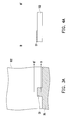
- FIG. 1A through FIG. 1E are schematic top views illustrating a method for fabricating a thin film transistor according to an embodiment of the present invention.
- FIG. 2A through FIG. 2E are schematic cross-sectional views illustrating a method for fabricating a thin film transistor according to an embodiment of the present invention.
- FIG. 3A through FIG. 3E are schematic top views illustrating a method for fabricating a thin film transistor according to another embodiment of the present invention.
- FIG. 4A through FIG. 4E are schematic cross-sectional views illustrating a method for fabricating a thin film transistor according to another embodiment of the present invention.
- FIG. 1A through FIG. 1E are schematic top views illustrating a method for fabricating a thin film transistor according to an embodiment of the present invention.
- FIG. 2A through FIG. 2E are schematic cross-sectional views illustrating a method for fabricating a thin film transistor according to an embodiment of the present invention.
- FIG. 2A through FIG. 2E are schematic cross-sectional views respectively corresponding to FIG. 1A through FIG. 1E along a along a section line A-A′.
- a substrate 102 is first provided.
- the substrate 102 is used to carry elements, and a material of the substrate 102 may be glass, quartz, organic polymer or any other opaque/reflective material (e.g. wafers or ceramics) or any other suitable material.
- a gate G is formed above the substrate 102 .
- a scan line SL electrically connected with the gate G may be further formed while forming the gate G.
- the gate G and the scan line SL are generally made of metallic materials, but the present invention is not limited thereto. In other embodiments, the gate G and the scan line SL may also be made of other conductive materials, such as an alloy, metal nitride, metal oxide, metal oxynitride, or a combination thereof.
- an insulation layer 104 may be formed.
- the insulation layer 104 covers the gate G.
- the insulation layer 104 may be made of inorganic materials (e.g. silicon oxide, silicon nitride or silicon oxynitride), an organic material or a combination thereof.
- a first source S 1 is then formed above the substrate 102 .
- a data line DL electrically connected with the first source S 1 may be further formed while forming the first source S 1 .
- the insulation layer 104 is located between the first source S 1 and the substrate 102 .
- the first source S 1 and the data line DL are generally made of metallic materials, but the present invention is not limited thereto. In other embodiments, the first source S 1 and the data line DL may also be made of other conductive materials, such as an alloy, metal nitride, metal oxide, metal oxynitride, or a combination thereof.
- a channel SE is formed afterward.
- One end SE- 1 of the channel SE contacts and is electrically connected with the first source S 1 .
- a material of the channel SE may be, for example, metal oxide semiconductor, such as indium-gallium-zinc oxide (IGZO), indium zinc oxide (IZO), indium gallium oxide (IGO), zinc oxide (ZnO), 2CdO.GeO 2 , or NiCo 2 O 4 , but the present invention is not limited thereto.
- an etch stop layer ESL is formed.
- the stop layer ESL at least covers the one end SE- 1 of the channel SE which contacts with the first source S 1 and exposes another end SE- 2 of the channel SE.
- the etch stop layer ESL is capable of protecting the channel SE therebelow, such that the channel SE will not be easily damaged in subsequent fabricating processes.
- the etch stop layer ESL is a complete pattern. In other words, the etch stop layer ESL does not contain any contact exposing the channel SE inside.
- a drain D is subsequently formed.
- the drain D contacts and is electrically connected with said another end SE- 2 of the channel SE.
- the fabrication of a thin film transistor TFT of the present embodiment is initially completed.
- a second source S 2 disconnected from the drain D may also be formed above the first source S 1 .
- the second source S 2 may entirely cover the first source S 1 .
- the second source S 2 is capable of protecting the first source S 1 therebelow, such that the first source S 1 will not be easily damaged during the process of forming the drain D.
- the present invention is not limited thereto. In other embodiments, the first source S 1 may be prevented from being damaged by adopting other means.
- different materials may be selected for fabricating the drain D and the first source S 1 .
- an etching solution having a great etching selectivity of the drain D to the first source S 1 may be selected for forming the drain D, such that first source S 1 will not be easily damaged during the process of forming the drain D.
- the second source S 2 may not have to be formed while forming the drain D.
- the thin film transistor TFT of the present embodiment includes the substrate 102 , the first source S 1 disposed above the substrate 102 , the channel SE, the etch stop layer ESL, the drain D and the gate G overlapping the channel SE.
- the one end SE- 1 of the channel SE contacts and is electrically connected with the first source S 1 .
- the one end SE- 1 of the channel SE may cover the first source S 1 .
- the first source S 1 is located between the channel SE and the substrate 102 .
- the etch stop layer ESL at least covers the one end SE- 1 of the channel SE which contacts with the first source S 1 and exposes said another end SE- 2 of the channel SE.
- each of the two ends SE- 1 and SE- 2 of the channel SE respectively has one of two edges of the channel SE, and the two edges may respectively cover the first source S 1 and be covered by the drain D.
- the first source S 1 and the drain D belong to different layers.
- the drain D and the first source S 1 are respectively located above an upper side and a lower side of the channel SE.
- the channel SE is located between the first source S 1 and the drain D.
- the first source S 1 , the channel SE, the etch stop layer ESL and the drain D may be stacked in sequence toward a direction that is away from the substrate 102 .
- the thin film transistor TFT of the present embodiment may selectively include the second source S 2 disconnected from the drain D.
- the second source S 2 is disposed above the first source S 1 and belongs to the same layer as the drain D.
- the second source S 2 may contact with the first source S 1 and be electrically connected therewith.
- the second source S 2 may entirely cover the first source S 1 .
- the second source S 2 may be aligned with the first source S 1 along a direction d in which the gate G and the channel SE are stacked.
- the drain D of the thin film transistor TFT and the first source S 1 are respectively formed above the upper side and the lower side of the channel SE and contact with the two ends of the channel SE.
- the channel SE does not have to retain the contact region exposed by the two contacts of the etch stop layer ESL like the way the conventional technique does. Accordingly, an effective length L of the channel SE may be significantly reduced, which facilitates in reducing the size of the thin film transistor TFT.
- the thin film transistor TFT of the present embodiment further includes the insulation layer 104 .
- the gate G may be disposed between the insulation layer 104 and the substrate 102 .
- the thin film transistor TFT of the present embodiment may be a bottom gate thin film transistor (bottom gate TFT).
- bottom gate TFT bottom gate thin film transistor
- the present invention is not limited thereto, and the conception of the present invention may also be applied to any other form of thin film transistor, such as a top gate thin film transistor (top gate TFT), which will be specifically described with reference to FIG. 3A through FIG. 3E and FIG. 4A through FIG. 4E .
- FIG. 3A through FIG. 3E are schematic top views illustrating a method for fabricating a thin film transistor according to another embodiment of the present invention.
- FIG. 4A through FIG. 4E are schematic cross-sectional views illustrating a method for fabricating a thin film transistor according to another embodiment of the present invention.
- FIG. 4A through FIG. 4E are schematic cross-sectional views respectively corresponding to FIG. 3A through FIG. 3E along a along a section line B-B′.
- the method for fabricating the thin film transistor illustrated in FIG. 3A through FIG. 3E and FIG. 4A through FIG. 4E is similar to that illustrated in FIG. 1A through FIG. 1E and FIG. 2A through FIG. 2E , and therefore, identical elements are labeled by the same numerals.
- a substrate 102 is first provided. Then, a first source S 1 is formed above the substrate 102 . Referring to FIG. 3B and FIG. 4B , a channel SE is then formed. One end SE- 1 of the channel SE contacts with the first source S 1 . Referring to FIG. 3C and FIG. 4C , an etch stop layer ESL is formed afterward. The etch stop layer ESL at least covers the one end SE- 1 of the channel SE which contacts with the first source S 1 and exposes another end SE- 2 of the channel SE.
- a drain D is formed.
- the drain D contacts with said another end SE- 2 of the channel SE.
- a second source S 2 may also be selectively formed above the first source S 1 while forming the drain D for protecting the first source S 1 during the process of forming the drain D.
- an insulation layer 106 is formed to cover the first source S 1 , the channel SE, the etch stop layer ESL and the drain D.
- a thin film transistor TFT 1 is similar to the thin film transistor TFT, and thus, identical elements are labeled by the same numerals.
- the thin film transistor TFT 1 includes the substrate 102 , the first source S 1 disposed above the substrate 102 , the channel SE, the etch stop layer ESL, the drain D and the gate G overlapping the channel SE.
- the one end SE- 1 of the channel SE contacts with the first source S 1 .
- the etch stop layer ESL at least covers the one end SE- 1 of the channel SE which contacts the first source S 1 and exposes said another end SE- 2 of the channel SE.
- the drain D contacts said another end SE- 2 of the channel SE.
- the thin film transistor TFT 1 of the present embodiment further includes the insulation layer 106 , and the insulation layer 106 is disposed between the gate G and the substrate 102 .
- the first source S 1 , the channel SE, the etch stop layer ESL, the drain D, the insulation layer 106 and the gate G are stacked in sequence toward a direction that is away from the substrate 102 .
- the thin film transistor TFT 1 may be a top gate thin film transistor (top gate TFT).
- the thin film transistor TFT 1 also has the same effect and advantages as the thin film transistor TFT, which will not be repeatedly described hereinafter.
- the drain of the thin film transistor the first source and the first source the drain of the thin film transistor are respectively formed above an upper side and a lower side of the channel and respectively contact with the two ends of the channel.
- the channel does not have to retain the contact region exposed by the two contacts like the way the conventional technique does. Accordingly, an effective length of the channel may be significantly reduced so as to facilitate in reducing the size of the thin film transistor.
- the second source disconnected from the drain can be formed above the first source while forming the drain.
- the second source can protect the first source therebelow during the process of forming the drain, such that the first source will not be easily damaged during the process of forming the drain. Accordingly, the thin film transistor can have a high yield.
Landscapes
- Engineering & Computer Science (AREA)
- Microelectronics & Electronic Packaging (AREA)
- Power Engineering (AREA)
- Physics & Mathematics (AREA)
- Ceramic Engineering (AREA)
- Condensed Matter Physics & Semiconductors (AREA)
- General Physics & Mathematics (AREA)
- Computer Hardware Design (AREA)
- Thin Film Transistor (AREA)
- Manufacturing & Machinery (AREA)
Applications Claiming Priority (3)
| Application Number | Priority Date | Filing Date | Title |
|---|---|---|---|
| TW102126709 | 2013-07-25 | ||
| TW102126709A | 2013-07-25 | ||
| TW102126709A TWI520221B (zh) | 2013-07-25 | 2013-07-25 | 薄膜電晶體及其製造方法 |
Publications (2)
| Publication Number | Publication Date |
|---|---|
| US8940590B1 true US8940590B1 (en) | 2015-01-27 |
| US20150028420A1 US20150028420A1 (en) | 2015-01-29 |
Family
ID=52350671
Family Applications (1)
| Application Number | Title | Priority Date | Filing Date |
|---|---|---|---|
| US14/018,448 Expired - Fee Related US8940590B1 (en) | 2013-07-25 | 2013-09-05 | Thin film transistor and method for fabricating the same |
Country Status (2)
| Country | Link |
|---|---|
| US (1) | US8940590B1 (zh) |
| TW (1) | TWI520221B (zh) |
Cited By (1)
| Publication number | Priority date | Publication date | Assignee | Title |
|---|---|---|---|---|
| EP3273485A4 (en) * | 2015-03-18 | 2019-04-03 | Boe Technology Group Co. Ltd. | THIN FILM TRANSISTOR AND METHOD FOR MANUFACTURING SAME, MATRIX SUBSTRATE, AND DISPLAY APPARATUS |
Citations (5)
| Publication number | Priority date | Publication date | Assignee | Title |
|---|---|---|---|---|
| US7442588B2 (en) | 2007-02-23 | 2008-10-28 | Silicon Display Technology Co., Ltd. | Method for fabricating thin film transistor using local oxidation and transparent thin film transistor |
| US20080303020A1 (en) * | 2007-05-29 | 2008-12-11 | Hyun-Soo Shin | Thin film transistor, flat panel display device having the same, and associated methods |
| TW200952178A (en) | 2008-06-10 | 2009-12-16 | Taiwan Tft Lcd Ass | Method for fabricating thin film transistor |
| US20110233536A1 (en) | 2010-03-24 | 2011-09-29 | Samsung Electronics Co., Ltd. | Thin film transistor array panel and method of fabricating the same |
| US20130313546A1 (en) * | 2012-05-24 | 2013-11-28 | Lg Display Co., Ltd. | Oxide Thin Film Transistor, Method for Fabricating TFT, Array Substrate for Display Device and Method for Fabricating the Same |
-
2013
- 2013-07-25 TW TW102126709A patent/TWI520221B/zh not_active IP Right Cessation
- 2013-09-05 US US14/018,448 patent/US8940590B1/en not_active Expired - Fee Related
Patent Citations (6)
| Publication number | Priority date | Publication date | Assignee | Title |
|---|---|---|---|---|
| US7442588B2 (en) | 2007-02-23 | 2008-10-28 | Silicon Display Technology Co., Ltd. | Method for fabricating thin film transistor using local oxidation and transparent thin film transistor |
| US20080303020A1 (en) * | 2007-05-29 | 2008-12-11 | Hyun-Soo Shin | Thin film transistor, flat panel display device having the same, and associated methods |
| US8053773B2 (en) * | 2007-05-29 | 2011-11-08 | Samsung Mobile Display Co., Ltd. | Thin film transistor, flat panel display device having the same, and associated methods |
| TW200952178A (en) | 2008-06-10 | 2009-12-16 | Taiwan Tft Lcd Ass | Method for fabricating thin film transistor |
| US20110233536A1 (en) | 2010-03-24 | 2011-09-29 | Samsung Electronics Co., Ltd. | Thin film transistor array panel and method of fabricating the same |
| US20130313546A1 (en) * | 2012-05-24 | 2013-11-28 | Lg Display Co., Ltd. | Oxide Thin Film Transistor, Method for Fabricating TFT, Array Substrate for Display Device and Method for Fabricating the Same |
Cited By (1)
| Publication number | Priority date | Publication date | Assignee | Title |
|---|---|---|---|---|
| EP3273485A4 (en) * | 2015-03-18 | 2019-04-03 | Boe Technology Group Co. Ltd. | THIN FILM TRANSISTOR AND METHOD FOR MANUFACTURING SAME, MATRIX SUBSTRATE, AND DISPLAY APPARATUS |
Also Published As
| Publication number | Publication date |
|---|---|
| TWI520221B (zh) | 2016-02-01 |
| US20150028420A1 (en) | 2015-01-29 |
| TW201505100A (zh) | 2015-02-01 |
Similar Documents
| Publication | Publication Date | Title |
|---|---|---|
| US8829511B2 (en) | Hybrid thin film transistor, manufacturing method thereof and display panel having the same | |
| KR102386458B1 (ko) | 유기 발광 표시 장치 및 그 제조 방법 | |
| US9660060B2 (en) | Thin film transistor and fabricating method thereof | |
| US11855103B2 (en) | Semiconductor device and method for manufacturing semiconductor device | |
| CN107658345B (zh) | 氧化物薄膜晶体管及其制备方法、阵列基板和显示装置 | |
| WO2016061940A1 (zh) | 薄膜晶体管阵列基板及其制作方法、显示装置 | |
| US9117768B2 (en) | Display substrate having a thin film transistor and method of manufacturing the same | |
| US9685466B2 (en) | Thin film transistor, array substrate and display device | |
| US11127859B2 (en) | Semiconductor device and manufacturing method thereof | |
| WO2018077065A1 (zh) | 薄膜晶体管及其制作方法、阵列基板、显示面板 | |
| EP2757589A2 (en) | Methods for fabricating a thin film transistor and an array substrate | |
| CN105932176B (zh) | 像素结构与其制造方法 | |
| US7923735B2 (en) | Thin film transistor and method of manufacturing the same | |
| WO2017028493A1 (zh) | 薄膜晶体管及其制作方法、显示器件 | |
| US8981377B2 (en) | Semiconductor device and method of making the same | |
| US8940590B1 (en) | Thin film transistor and method for fabricating the same | |
| KR101909704B1 (ko) | 표시 기판 및 이의 제조 방법 | |
| US20150084036A1 (en) | Thin film transistor and fabricating method thereof | |
| KR102522595B1 (ko) | 트랜지스터 패널 및 그 제조 방법 | |
| US20150325700A1 (en) | Thin film transistor and pixel structure | |
| US20150102345A1 (en) | Active device and manufacturing method thereof | |
| KR102570469B1 (ko) | 박막 트랜지스터 및 표시 장치 | |
| KR20150086022A (ko) | 박막 트랜지스터 및 이의 제조 방법 | |
| KR20150019137A (ko) | 고 이동도 박막 트랜지스터 및 그 제조방법과 고 이동도 박막 트랜지스터를 포함하는 디스플레이 | |
| US9455351B1 (en) | Oxide semiconductor field effect transistor device and method for manufacturing the same |
Legal Events
| Date | Code | Title | Description |
|---|---|---|---|
| AS | Assignment |
Owner name: CHUNGHWA PICTURE TUBES, LTD., TAIWAN Free format text: ASSIGNMENT OF ASSIGNORS INTEREST;ASSIGNORS:HUANG, YEN-YU;CHANG, HSI-MING;REEL/FRAME:031171/0015 Effective date: 20130902 |
|
| STCF | Information on status: patent grant |
Free format text: PATENTED CASE |
|
| MAFP | Maintenance fee payment |
Free format text: PAYMENT OF MAINTENANCE FEE, 4TH YEAR, LARGE ENTITY (ORIGINAL EVENT CODE: M1551) Year of fee payment: 4 |
|
| FEPP | Fee payment procedure |
Free format text: MAINTENANCE FEE REMINDER MAILED (ORIGINAL EVENT CODE: REM.); ENTITY STATUS OF PATENT OWNER: LARGE ENTITY |
|
| LAPS | Lapse for failure to pay maintenance fees |
Free format text: PATENT EXPIRED FOR FAILURE TO PAY MAINTENANCE FEES (ORIGINAL EVENT CODE: EXP.); ENTITY STATUS OF PATENT OWNER: LARGE ENTITY |
|
| STCH | Information on status: patent discontinuation |
Free format text: PATENT EXPIRED DUE TO NONPAYMENT OF MAINTENANCE FEES UNDER 37 CFR 1.362 |
|
| FP | Lapsed due to failure to pay maintenance fee |
Effective date: 20230127 |