US8928795B2 - Backside illumination image sensor and image-capturing device - Google Patents
Backside illumination image sensor and image-capturing device Download PDFInfo
- Publication number
- US8928795B2 US8928795B2 US13/033,187 US201113033187A US8928795B2 US 8928795 B2 US8928795 B2 US 8928795B2 US 201113033187 A US201113033187 A US 201113033187A US 8928795 B2 US8928795 B2 US 8928795B2
- Authority
- US
- United States
- Prior art keywords
- light shielding
- chip lens
- photoelectric conversion
- shielding film
- conversion elements
- Prior art date
- Legal status (The legal status is an assumption and is not a legal conclusion. Google has not performed a legal analysis and makes no representation as to the accuracy of the status listed.)
- Active, expires
Links
Images




Classifications
-
- H01L27/14623—
-
- H—ELECTRICITY
- H04—ELECTRIC COMMUNICATION TECHNIQUE
- H04N—PICTORIAL COMMUNICATION, e.g. TELEVISION
- H04N25/00—Circuitry of solid-state image sensors [SSIS]; Control thereof
- H04N25/10—Circuitry of solid-state image sensors [SSIS]; Control thereof for transforming different wavelengths into image signals
- H04N25/11—Arrangement of colour filter arrays [CFA]; Filter mosaics
- H04N25/13—Arrangement of colour filter arrays [CFA]; Filter mosaics characterised by the spectral characteristics of the filter elements
- H04N25/134—Arrangement of colour filter arrays [CFA]; Filter mosaics characterised by the spectral characteristics of the filter elements based on three different wavelength filter elements
-
- H01L27/14627—
-
- H—ELECTRICITY
- H04—ELECTRIC COMMUNICATION TECHNIQUE
- H04N—PICTORIAL COMMUNICATION, e.g. TELEVISION
- H04N23/00—Cameras or camera modules comprising electronic image sensors; Control thereof
- H04N23/60—Control of cameras or camera modules
- H04N23/63—Control of cameras or camera modules by using electronic viewfinders
-
- H—ELECTRICITY
- H04—ELECTRIC COMMUNICATION TECHNIQUE
- H04N—PICTORIAL COMMUNICATION, e.g. TELEVISION
- H04N25/00—Circuitry of solid-state image sensors [SSIS]; Control thereof
- H04N25/70—SSIS architectures; Circuits associated therewith
- H04N25/703—SSIS architectures incorporating pixels for producing signals other than image signals
- H04N25/704—Pixels specially adapted for focusing, e.g. phase difference pixel sets
-
- H04N5/3696—
-
- H04N9/045—
-
- H—ELECTRICITY
- H10—SEMICONDUCTOR DEVICES; ELECTRIC SOLID-STATE DEVICES NOT OTHERWISE PROVIDED FOR
- H10F—INORGANIC SEMICONDUCTOR DEVICES SENSITIVE TO INFRARED RADIATION, LIGHT, ELECTROMAGNETIC RADIATION OF SHORTER WAVELENGTH OR CORPUSCULAR RADIATION
- H10F39/00—Integrated devices, or assemblies of multiple devices, comprising at least one element covered by group H10F30/00, e.g. radiation detectors comprising photodiode arrays
- H10F39/10—Integrated devices
- H10F39/12—Image sensors
- H10F39/18—Complementary metal-oxide-semiconductor [CMOS] image sensors; Photodiode array image sensors
- H10F39/182—Colour image sensors
-
- H—ELECTRICITY
- H10—SEMICONDUCTOR DEVICES; ELECTRIC SOLID-STATE DEVICES NOT OTHERWISE PROVIDED FOR
- H10F—INORGANIC SEMICONDUCTOR DEVICES SENSITIVE TO INFRARED RADIATION, LIGHT, ELECTROMAGNETIC RADIATION OF SHORTER WAVELENGTH OR CORPUSCULAR RADIATION
- H10F39/00—Integrated devices, or assemblies of multiple devices, comprising at least one element covered by group H10F30/00, e.g. radiation detectors comprising photodiode arrays
- H10F39/10—Integrated devices
- H10F39/12—Image sensors
- H10F39/199—Back-illuminated image sensors
-
- H—ELECTRICITY
- H10—SEMICONDUCTOR DEVICES; ELECTRIC SOLID-STATE DEVICES NOT OTHERWISE PROVIDED FOR
- H10F—INORGANIC SEMICONDUCTOR DEVICES SENSITIVE TO INFRARED RADIATION, LIGHT, ELECTROMAGNETIC RADIATION OF SHORTER WAVELENGTH OR CORPUSCULAR RADIATION
- H10F39/00—Integrated devices, or assemblies of multiple devices, comprising at least one element covered by group H10F30/00, e.g. radiation detectors comprising photodiode arrays
- H10F39/80—Constructional details of image sensors
- H10F39/802—Geometry or disposition of elements in pixels, e.g. address-lines or gate electrodes
- H10F39/8023—Disposition of the elements in pixels, e.g. smaller elements in the centre of the imager compared to larger elements at the periphery
-
- H—ELECTRICITY
- H10—SEMICONDUCTOR DEVICES; ELECTRIC SOLID-STATE DEVICES NOT OTHERWISE PROVIDED FOR
- H10F—INORGANIC SEMICONDUCTOR DEVICES SENSITIVE TO INFRARED RADIATION, LIGHT, ELECTROMAGNETIC RADIATION OF SHORTER WAVELENGTH OR CORPUSCULAR RADIATION
- H10F39/00—Integrated devices, or assemblies of multiple devices, comprising at least one element covered by group H10F30/00, e.g. radiation detectors comprising photodiode arrays
- H10F39/80—Constructional details of image sensors
- H10F39/805—Coatings
- H10F39/8053—Colour filters
-
- H—ELECTRICITY
- H10—SEMICONDUCTOR DEVICES; ELECTRIC SOLID-STATE DEVICES NOT OTHERWISE PROVIDED FOR
- H10F—INORGANIC SEMICONDUCTOR DEVICES SENSITIVE TO INFRARED RADIATION, LIGHT, ELECTROMAGNETIC RADIATION OF SHORTER WAVELENGTH OR CORPUSCULAR RADIATION
- H10F39/00—Integrated devices, or assemblies of multiple devices, comprising at least one element covered by group H10F30/00, e.g. radiation detectors comprising photodiode arrays
- H10F39/80—Constructional details of image sensors
- H10F39/805—Coatings
- H10F39/8057—Optical shielding
-
- H—ELECTRICITY
- H10—SEMICONDUCTOR DEVICES; ELECTRIC SOLID-STATE DEVICES NOT OTHERWISE PROVIDED FOR
- H10F—INORGANIC SEMICONDUCTOR DEVICES SENSITIVE TO INFRARED RADIATION, LIGHT, ELECTROMAGNETIC RADIATION OF SHORTER WAVELENGTH OR CORPUSCULAR RADIATION
- H10F39/00—Integrated devices, or assemblies of multiple devices, comprising at least one element covered by group H10F30/00, e.g. radiation detectors comprising photodiode arrays
- H10F39/80—Constructional details of image sensors
- H10F39/806—Optical elements or arrangements associated with the image sensors
- H10F39/8063—Microlenses
-
- H—ELECTRICITY
- H10—SEMICONDUCTOR DEVICES; ELECTRIC SOLID-STATE DEVICES NOT OTHERWISE PROVIDED FOR
- H10F—INORGANIC SEMICONDUCTOR DEVICES SENSITIVE TO INFRARED RADIATION, LIGHT, ELECTROMAGNETIC RADIATION OF SHORTER WAVELENGTH OR CORPUSCULAR RADIATION
- H10F39/00—Integrated devices, or assemblies of multiple devices, comprising at least one element covered by group H10F30/00, e.g. radiation detectors comprising photodiode arrays
- H10F39/80—Constructional details of image sensors
- H10F39/807—Pixel isolation structures
-
- H01L27/14621—
Definitions
- the body drive control device 214 calculates the defocus amount indicating the extent of defocusing based upon pixel signals output from the focus detection pixels at the image sensor 212 and transmits this defocus amount to the lens drive control device 206 .
- the body drive control device 214 generates image data by processing the pixel signals originating from the image-capturing pixels at the image sensor 212 and stores the image data thus generated into the memory card 219 . It also provides live view image signals read out from the image sensor 212 to the liquid crystal display element drive circuit 215 so as to bring up a live view image on display at the liquid crystal display element 216 .
- the body drive control device 214 provides aperture control information to the lens drive control device 206 to enable opening control of the aperture 211 .
- FIG. 6C shows the focus detection pixel 315 in a front view. Its on-chip lens 10 assumes a square shape. An opening 15 , formed at a light shielding film to be described later, limits the light receiving area of the photoelectric conversion element to a left half of a square (the left half of a square split into two equal portions along a vertical line).
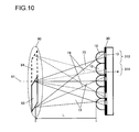
- each image-capturing pixel 310 receives a light flux 71 having passed through the area 95 and the on-chip lens 10 at the particular image-capturing pixel 310 , and then outputs a signal corresponding to the intensity of the image formed with the light flux 71 on the on-chip lens 10 .
- the distance D from the apex T of the on-chip lens 10 to the plane at which the light shielding film 30 is disposed must be determined so as to satisfy the relationships defined in expressions (3) and (6).
- the average refractive index n for the on-chip lens 10 and the medium present between the on-chip lens 10 and the light shielding film 30 , the pixel pitch P and the smallest F number F 0 may be respectively 1.5, 4 ⁇ m and 1.4.
- stray light 21 with a large angle of incidence is bound to pass through two different types of color filters 9 , before it ever reaches the opening 11 in an adjacent unit pixel area 403 .
- two different types of color filters 9 achieve spectral sensitivity characteristics different from each other. For this reason, the light will have been fully attenuated by the time it reaches the opening 11 of the adjacent unit pixel area 403 , and since color mixture (crosstalk) is thus prevented, an image of high quality can be generated.
- an image-capturing signal equivalent to an image-capturing signal that would be output at an image-capturing pixel 310 equipped with a G-color filter taking up the particular focus detection pixel position can be generated by adding the signal from the photoelectric conversion elements 43 and the signal from the photoelectric conversion element 44 .
- an image-capturing signal equivalent to an image-capturing signal that would be output at an image-capturing pixel 310 equipped with an R-color filter taking up the particular focus detection pixel position can be generated by adding the signal from the photoelectric conversion elements 43 and the signal from the photoelectric conversion element 44 .
Landscapes
- Engineering & Computer Science (AREA)
- Multimedia (AREA)
- Signal Processing (AREA)
- Physics & Mathematics (AREA)
- Spectroscopy & Molecular Physics (AREA)
- Solid State Image Pick-Up Elements (AREA)
- Transforming Light Signals Into Electric Signals (AREA)
Abstract
Description
D=R·n/(n−n0) (1)
D=R·n/(n−1) (2)
D>P·n/(2·(n−1)) (3)
S=(Q·(D−R))/(L+R) (4)
S=(D−R)/F (5)
D<F0·P·n (6)
Claims (5)
D=R·n/(n−1).
F0·P·n>D>P·n/(2·(n−1)).
Priority Applications (9)
| Application Number | Priority Date | Filing Date | Title |
|---|---|---|---|
| US14/555,868 US9184197B2 (en) | 2010-02-25 | 2014-11-28 | Backside illumination image sensor and image-capturing device |
| US14/877,439 US9466633B2 (en) | 2010-02-25 | 2015-10-07 | Backside illumination image sensor and image-capturing device |
| US15/260,994 US9704902B2 (en) | 2010-02-25 | 2016-09-09 | Backside illumination image sensor and image-capturing device |
| US15/615,188 US10204949B2 (en) | 2010-02-25 | 2017-06-06 | Backside illumination image sensor and image-capturing device |
| US16/238,110 US10777595B2 (en) | 2010-02-25 | 2019-01-02 | Backside illumination image sensor and image-capturing device |
| US16/995,314 US11601624B2 (en) | 2010-02-25 | 2020-08-17 | Backside illumination image sensor and image-capturing device |
| US18/104,819 US11979672B2 (en) | 2010-02-25 | 2023-02-02 | Backside illumination image sensor and image-capturing device |
| US18/627,723 US20240251179A1 (en) | 2010-02-25 | 2024-04-05 | Backside illumination image sensor and image-capturing device |
| US19/169,127 US20250260907A1 (en) | 2010-02-25 | 2025-04-03 | Backside illumination image sensor and image-capturing device |
Applications Claiming Priority (2)
| Application Number | Priority Date | Filing Date | Title |
|---|---|---|---|
| JP2010-040378 | 2010-02-25 | ||
| JP2010040378A JP2011176715A (en) | 2010-02-25 | 2010-02-25 | Back-illuminated image sensor and imaging apparatus |
Related Child Applications (1)
| Application Number | Title | Priority Date | Filing Date |
|---|---|---|---|
| US14/555,868 Continuation US9184197B2 (en) | 2010-02-25 | 2014-11-28 | Backside illumination image sensor and image-capturing device |
Publications (2)
| Publication Number | Publication Date |
|---|---|
| US20110279727A1 US20110279727A1 (en) | 2011-11-17 |
| US8928795B2 true US8928795B2 (en) | 2015-01-06 |
Family
ID=44689142
Family Applications (10)
| Application Number | Title | Priority Date | Filing Date |
|---|---|---|---|
| US13/033,187 Active 2033-09-16 US8928795B2 (en) | 2010-02-25 | 2011-02-23 | Backside illumination image sensor and image-capturing device |
| US14/555,868 Active US9184197B2 (en) | 2010-02-25 | 2014-11-28 | Backside illumination image sensor and image-capturing device |
| US14/877,439 Active US9466633B2 (en) | 2010-02-25 | 2015-10-07 | Backside illumination image sensor and image-capturing device |
| US15/260,994 Active US9704902B2 (en) | 2010-02-25 | 2016-09-09 | Backside illumination image sensor and image-capturing device |
| US15/615,188 Active US10204949B2 (en) | 2010-02-25 | 2017-06-06 | Backside illumination image sensor and image-capturing device |
| US16/238,110 Active US10777595B2 (en) | 2010-02-25 | 2019-01-02 | Backside illumination image sensor and image-capturing device |
| US16/995,314 Active US11601624B2 (en) | 2010-02-25 | 2020-08-17 | Backside illumination image sensor and image-capturing device |
| US18/104,819 Active US11979672B2 (en) | 2010-02-25 | 2023-02-02 | Backside illumination image sensor and image-capturing device |
| US18/627,723 Abandoned US20240251179A1 (en) | 2010-02-25 | 2024-04-05 | Backside illumination image sensor and image-capturing device |
| US19/169,127 Pending US20250260907A1 (en) | 2010-02-25 | 2025-04-03 | Backside illumination image sensor and image-capturing device |
Family Applications After (9)
| Application Number | Title | Priority Date | Filing Date |
|---|---|---|---|
| US14/555,868 Active US9184197B2 (en) | 2010-02-25 | 2014-11-28 | Backside illumination image sensor and image-capturing device |
| US14/877,439 Active US9466633B2 (en) | 2010-02-25 | 2015-10-07 | Backside illumination image sensor and image-capturing device |
| US15/260,994 Active US9704902B2 (en) | 2010-02-25 | 2016-09-09 | Backside illumination image sensor and image-capturing device |
| US15/615,188 Active US10204949B2 (en) | 2010-02-25 | 2017-06-06 | Backside illumination image sensor and image-capturing device |
| US16/238,110 Active US10777595B2 (en) | 2010-02-25 | 2019-01-02 | Backside illumination image sensor and image-capturing device |
| US16/995,314 Active US11601624B2 (en) | 2010-02-25 | 2020-08-17 | Backside illumination image sensor and image-capturing device |
| US18/104,819 Active US11979672B2 (en) | 2010-02-25 | 2023-02-02 | Backside illumination image sensor and image-capturing device |
| US18/627,723 Abandoned US20240251179A1 (en) | 2010-02-25 | 2024-04-05 | Backside illumination image sensor and image-capturing device |
| US19/169,127 Pending US20250260907A1 (en) | 2010-02-25 | 2025-04-03 | Backside illumination image sensor and image-capturing device |
Country Status (2)
| Country | Link |
|---|---|
| US (10) | US8928795B2 (en) |
| JP (1) | JP2011176715A (en) |
Cited By (10)
| Publication number | Priority date | Publication date | Assignee | Title |
|---|---|---|---|---|
| US20150084146A1 (en) * | 2010-02-25 | 2015-03-26 | Nikon Corporation | Backside illumination image sensor and image-capturing device |
| US9704905B2 (en) | 2012-12-10 | 2017-07-11 | Canon Kabushiki Kaisha | Solid-state image sensor and method of manufacturing the same |
| US9773827B2 (en) | 2011-10-03 | 2017-09-26 | Canon Kabushiki Kaisha | Solid-state image sensor and camera where the plurality of pixels form a pixel group under a single microlens |
| US9876044B2 (en) | 2015-12-15 | 2018-01-23 | Samsung Electronics Co., Ltd. | Image sensor and method of manufacturing the same |
| US10910427B2 (en) | 2015-12-28 | 2021-02-02 | Semiconductor Energy Laboratory Co., Ltd. | Imaging device and electronic device |
| US11405576B2 (en) * | 2012-09-27 | 2022-08-02 | Nikon Corporation | Image sensor and image-capturing device |
| US11488996B2 (en) | 2014-08-29 | 2022-11-01 | Samsung Electronics Co., Ltd. | Image sensor and manufacturing method thereof |
| US12219861B2 (en) | 2021-07-20 | 2025-02-04 | Semiconductor Energy Laboratory Co., Ltd. | Display apparatus and electronic device |
| US12376410B2 (en) | 2019-07-04 | 2025-07-29 | Semiconductor Energy Laboratory Co., Ltd. | Imaging device with embedded conductive layers |
| US12648251B2 (en) | 2021-06-17 | 2026-06-02 | Semiconductor Energy Laboratory Co., Ltd. | Imaging device and electronic device |
Families Citing this family (90)
| Publication number | Priority date | Publication date | Assignee | Title |
|---|---|---|---|---|
| JP2011109200A (en) * | 2009-11-13 | 2011-06-02 | Sanyo Electric Co Ltd | Surveillance camera |
| JP5825817B2 (en) * | 2011-04-01 | 2015-12-02 | キヤノン株式会社 | Solid-state imaging device and imaging apparatus |
| JP2013016676A (en) * | 2011-07-05 | 2013-01-24 | Sony Corp | Solid state image pickup device, manufacturing method of the same and electronic apparatus |
| US8878969B2 (en) * | 2011-07-27 | 2014-11-04 | Aptina Imaging Corporation | Imaging systems with color filter barriers |
| JP5794068B2 (en) * | 2011-09-16 | 2015-10-14 | ソニー株式会社 | Solid-state imaging device, manufacturing method, and electronic apparatus |
| JP5746606B2 (en) * | 2011-12-14 | 2015-07-08 | 日本放送協会 | Hologram reproducing method, apparatus and hologram recording / reproducing apparatus |
| JP5810173B2 (en) * | 2011-12-21 | 2015-11-11 | シャープ株式会社 | Imaging apparatus and electronic information device |
| JP5774501B2 (en) * | 2012-01-12 | 2015-09-09 | 株式会社東芝 | Solid-state imaging device |
| JP2013145779A (en) * | 2012-01-13 | 2013-07-25 | Sony Corp | Solid-state imaging device and electronic apparatus |
| JP6137804B2 (en) * | 2012-01-13 | 2017-05-31 | キヤノン株式会社 | Imaging apparatus and control method thereof, and lens unit and control method thereof |
| JP6095268B2 (en) | 2012-02-24 | 2017-03-15 | キヤノン株式会社 | Solid-state imaging device and imaging system |
| JP5542247B2 (en) * | 2012-03-30 | 2014-07-09 | 富士フイルム株式会社 | Imaging device and imaging apparatus |
| JP6051570B2 (en) * | 2012-04-12 | 2016-12-27 | 株式会社ニコン | Imaging device and imaging apparatus |
| JP5781021B2 (en) * | 2012-06-14 | 2015-09-16 | キヤノン株式会社 | LENS DEVICE AND IMAGING DEVICE |
| KR20130142000A (en) * | 2012-06-18 | 2013-12-27 | 삼성전자주식회사 | Image sensor, image processing device having the same, and method for manufacturing the same |
| JP5942757B2 (en) | 2012-09-28 | 2016-06-29 | 株式会社ニコン | Focus detection apparatus and imaging apparatus |
| JP6308717B2 (en) * | 2012-10-16 | 2018-04-11 | キヤノン株式会社 | Solid-state imaging device, method for manufacturing solid-state imaging device, and imaging system |
| JP6288909B2 (en) * | 2012-10-19 | 2018-03-07 | キヤノン株式会社 | Imaging device and imaging apparatus |
| JP6120523B2 (en) | 2012-10-24 | 2017-04-26 | オリンパス株式会社 | Imaging device and imaging apparatus |
| JP6234024B2 (en) | 2012-11-21 | 2017-11-22 | オリンパス株式会社 | Imaging device and imaging apparatus |
| DE112013005594T5 (en) * | 2012-11-22 | 2015-10-22 | Fujifilm Corporation | Imaging device, blur amount calculation method and lens device |
| EP2782331A1 (en) * | 2013-03-22 | 2014-09-24 | Harvest Imaging bvba | Image sensor with focus-detection pixel, and method for reading focus-information |
| TWI620445B (en) * | 2013-03-25 | 2018-04-01 | 新力股份有限公司 | Camera element and electronic equipment |
| CN103296042A (en) * | 2013-05-30 | 2013-09-11 | 豪威科技(上海)有限公司 | Backside-illuminated CMOS (complementary metal oxide semiconductor) image sensor and production method thereof |
| JP6103301B2 (en) * | 2013-07-03 | 2017-03-29 | ソニー株式会社 | Solid-state imaging device, manufacturing method thereof, and electronic apparatus |
| TWI623232B (en) * | 2013-07-05 | 2018-05-01 | 新力股份有限公司 | Solid-state imaging device, driving method thereof, and electronic device including solid-state imaging device |
| JP6295526B2 (en) * | 2013-07-11 | 2018-03-20 | ソニー株式会社 | Solid-state imaging device and electronic apparatus |
| JP2015026675A (en) * | 2013-07-25 | 2015-02-05 | ソニー株式会社 | Solid-state imaging device, manufacturing method thereof, and electronic device |
| JP2015037158A (en) * | 2013-08-15 | 2015-02-23 | ソニー株式会社 | Solid-state imaging element, electronic apparatus, and inspection device |
| JP6108172B2 (en) | 2013-09-02 | 2017-04-05 | ソニー株式会社 | Solid-state imaging device, manufacturing method thereof, and electronic device |
| JP2015056417A (en) * | 2013-09-10 | 2015-03-23 | ソニー株式会社 | Imaging device, manufacturing apparatus, manufacturing method and electronic apparatus |
| EP3051811A4 (en) * | 2013-09-26 | 2017-03-22 | Nikon Corporation | Image pickup element and image pickup device |
| CN103474444A (en) * | 2013-09-29 | 2013-12-25 | 武汉新芯集成电路制造有限公司 | Backside illuminated CMOS image sensor |
| TW201514599A (en) * | 2013-10-07 | 2015-04-16 | Novatek Microelectronics Corp | Image sensor and image capturing system |
| JP2015144194A (en) | 2014-01-31 | 2015-08-06 | ソニー株式会社 | Solid-state imaging device and electronic device |
| JP2015167219A (en) * | 2014-02-13 | 2015-09-24 | ソニー株式会社 | Image pickup device, manufacturing apparatus and electronic apparatus |
| JP6315776B2 (en) * | 2014-02-20 | 2018-04-25 | オリンパス株式会社 | Imaging device, imaging device |
| US9392198B2 (en) * | 2014-02-26 | 2016-07-12 | Semiconductor Components Industries, Llc | Backside illuminated imaging systems having auto-focus pixels |
| JP2015195235A (en) * | 2014-03-31 | 2015-11-05 | ソニー株式会社 | Solid state image sensor, electronic apparatus and imaging method |
| JP6237431B2 (en) * | 2014-04-15 | 2017-11-29 | ソニー株式会社 | Focus detection device, electronic equipment |
| JP6179776B2 (en) * | 2014-06-09 | 2017-08-16 | ソニー株式会社 | Imaging device, electronic device, and manufacturing method |
| US9640576B2 (en) * | 2014-08-20 | 2017-05-02 | Visera Technologies Company Limited | Image sensing device and method for fabricating the same |
| JP2016051746A (en) * | 2014-08-29 | 2016-04-11 | ソニー株式会社 | Solid-state imaging device and electronic device |
| JP6369233B2 (en) * | 2014-09-01 | 2018-08-08 | ソニー株式会社 | Solid-state imaging device, signal processing method thereof, and electronic device |
| JP2016058451A (en) * | 2014-09-05 | 2016-04-21 | キヤノン株式会社 | Sensor and camera |
| CN106068563B (en) | 2015-01-13 | 2022-01-14 | 索尼半导体解决方案公司 | Solid-state imaging device, method of manufacturing solid-state imaging device, and electronic apparatus |
| DE112015005847T5 (en) * | 2015-01-23 | 2017-09-14 | Olympus Corporation | Endoscope apparatus and focus control method for endoscope apparatus |
| JP6566734B2 (en) * | 2015-06-11 | 2019-08-28 | キヤノン株式会社 | Solid-state image sensor |
| JP6545016B2 (en) * | 2015-06-25 | 2019-07-17 | 三重富士通セミコンダクター株式会社 | Solid-state imaging device and light shielding method |
| WO2017039038A1 (en) * | 2015-09-04 | 2017-03-09 | 재단법인 다차원 스마트 아이티 융합시스템 연구단 | Image sensor to which multiple fill factors are applied |
| JP6178835B2 (en) * | 2015-12-22 | 2017-08-09 | キヤノン株式会社 | Solid-state imaging device and camera |
| CN118281017A (en) | 2015-12-25 | 2024-07-02 | 株式会社尼康 | Filming equipment |
| JP6740628B2 (en) * | 2016-02-12 | 2020-08-19 | 凸版印刷株式会社 | Solid-state image sensor and manufacturing method thereof |
| US20190063909A1 (en) * | 2016-03-23 | 2019-02-28 | Enplas Corporation | Marker |
| CN113489904B (en) * | 2016-07-13 | 2023-07-21 | 索尼公司 | Imaging device, imaging device and image processing device |
| KR102762966B1 (en) * | 2016-08-30 | 2025-02-05 | 삼성전자주식회사 | Image sensor and driving method thereof |
| JP6833430B2 (en) * | 2016-09-27 | 2021-02-24 | 東芝情報システム株式会社 | Manufacturing method of solid-state image sensor |
| JP2018056521A (en) * | 2016-09-30 | 2018-04-05 | 株式会社ニコン | Imaging device and imaging apparatus |
| JP6648666B2 (en) * | 2016-09-30 | 2020-02-14 | 株式会社ニコン | Image sensor and focus adjustment device |
| US10847559B2 (en) * | 2016-10-12 | 2020-11-24 | Sony Semiconductor Solutions Corporation | Solid-state image sensor and electronic device |
| JP6316902B2 (en) * | 2016-10-28 | 2018-04-25 | ソニー株式会社 | Solid-state imaging device and electronic device |
| JP2017092499A (en) * | 2017-02-10 | 2017-05-25 | キヤノン株式会社 | Solid state imaging device and imaging system |
| KR102350605B1 (en) | 2017-04-17 | 2022-01-14 | 삼성전자주식회사 | Image sensor |
| US11217617B2 (en) * | 2017-06-21 | 2022-01-04 | Sony Semiconductor Solutions Corporation | Imaging element and solid-state imaging device |
| JP2019012968A (en) | 2017-06-30 | 2019-01-24 | ソニーセミコンダクタソリューションズ株式会社 | Solid-state imaging device and electronic device |
| JP6526115B2 (en) * | 2017-07-13 | 2019-06-05 | キヤノン株式会社 | Solid-state imaging device |
| JP6506814B2 (en) * | 2017-10-18 | 2019-04-24 | キヤノン株式会社 | Solid-state imaging device and camera |
| JP2019087659A (en) * | 2017-11-08 | 2019-06-06 | ソニーセミコンダクタソリューションズ株式会社 | Image sensor, method of manufacturing the same, and electronic device |
| JP6779929B2 (en) | 2018-02-09 | 2020-11-04 | キヤノン株式会社 | Photoelectric converters and equipment |
| KR102025012B1 (en) * | 2018-05-08 | 2019-09-24 | 재단법인 다차원 스마트 아이티 융합시스템 연구단 | Multi pixel micro lens pixel array and camera system for solving color mix and operating method thereof |
| WO2020044928A1 (en) * | 2018-08-31 | 2020-03-05 | ソニーセミコンダクタソリューションズ株式会社 | Imaging element, imaging device, and imaging method |
| US20220068991A1 (en) * | 2018-12-27 | 2022-03-03 | Sony Semiconductor Solutions Corporation | Imaging element and manufacturing method of imaging element |
| WO2020195825A1 (en) * | 2019-03-25 | 2020-10-01 | ソニーセミコンダクタソリューションズ株式会社 | Imaging device and electronic apparatus |
| JP2020161648A (en) * | 2019-03-27 | 2020-10-01 | ソニーセミコンダクタソリューションズ株式会社 | Image sensor and image sensor |
| JP6744943B2 (en) * | 2019-03-29 | 2020-08-19 | キヤノン株式会社 | Solid-state imaging device and camera |
| TWI853915B (en) * | 2019-05-10 | 2024-09-01 | 日商索尼半導體解決方案公司 | Photographic components and electronic equipment |
| TWI688088B (en) * | 2019-07-24 | 2020-03-11 | 晶相光電股份有限公司 | Image sensing device and image sensing system |
| KR102664446B1 (en) | 2019-08-28 | 2024-05-09 | 에스케이하이닉스 주식회사 | Image sensing device |
| TWI739431B (en) * | 2019-12-09 | 2021-09-11 | 大陸商廣州印芯半導體技術有限公司 | Data transmission system and data transmission method thereof |
| US11343435B2 (en) * | 2019-12-26 | 2022-05-24 | Waymo Llc | Microlensing for real-time sensing of stray light |
| US12434172B2 (en) | 2020-09-22 | 2025-10-07 | The Usa, As Represented By The Secretary, Dept. Of Health And Human Services | Methods and systems for managing fluid flow in containers |
| JPWO2022080168A1 (en) * | 2020-10-15 | 2022-04-21 | ||
| JP7889792B2 (en) * | 2020-11-24 | 2026-07-14 | 三星電子株式会社 | Image sensor |
| JP2022091358A (en) * | 2020-12-09 | 2022-06-21 | ソニーセミコンダクタソリューションズ株式会社 | Imaging apparatus and electronic apparatus |
| KR102804387B1 (en) * | 2020-12-30 | 2025-05-07 | 에스케이하이닉스 주식회사 | Image Sensor, Test System and Method of Image Sensor Using the Same |
| DE112022002630T5 (en) * | 2021-05-17 | 2024-03-14 | Sony Semiconductor Solutions Corporation | IMAGING ELEMENT AND ELECTRONIC DEVICE |
| JP2023006303A (en) * | 2021-06-30 | 2023-01-18 | ソニーセミコンダクタソリューションズ株式会社 | Solid-state imaging element, manufacturing method, and electronic device |
| US12369416B2 (en) * | 2021-10-01 | 2025-07-22 | Visera Technologies Company Limited | Image sensor having dish structure formed within micro-lens |
| WO2025084019A1 (en) * | 2023-10-19 | 2025-04-24 | ソニーセミコンダクタソリューションズ株式会社 | Light detection device |
| US20250261457A1 (en) * | 2024-02-13 | 2025-08-14 | Shenzhen Adaps Photonics Technology Co., Ltd. | 3d stacked apd/spad for visible light operating at high speed |
Citations (23)
| Publication number | Priority date | Publication date | Assignee | Title |
|---|---|---|---|---|
| JPH11186530A (en) | 1997-12-25 | 1999-07-09 | Sony Corp | Micro lens formation method |
| JP2003051585A (en) | 2001-08-03 | 2003-02-21 | Sony Corp | Solid-state imaging device and method of manufacturing the same |
| WO2004008196A1 (en) | 2002-07-13 | 2004-01-22 | Autocloning Technology Ltd. | Polarization analyzer |
| JP3592147B2 (en) | 1998-08-20 | 2004-11-24 | キヤノン株式会社 | Solid-state imaging device |
| JP2005209676A (en) | 2004-01-20 | 2005-08-04 | Sony Corp | Solid-state imaging device and method for manufacturing solid-state imaging device |
| JP2005294647A (en) | 2004-04-01 | 2005-10-20 | Matsushita Electric Ind Co Ltd | Solid-state imaging device and manufacturing method thereof |
| JP2006019653A (en) | 2004-07-05 | 2006-01-19 | Sony Corp | Solid-state imaging device |
| JP2006080457A (en) | 2004-09-13 | 2006-03-23 | Sony Corp | Solid-state imaging device and manufacturing method thereof |
| WO2006046396A1 (en) | 2004-10-28 | 2006-05-04 | Matsushita Electric Industrial Co., Ltd. | Camera module |
| JP2007088057A (en) | 2005-09-20 | 2007-04-05 | Fujifilm Corp | Solid-state imaging device and manufacturing method thereof |
| JP2007155930A (en) | 2005-12-01 | 2007-06-21 | Nikon Corp | Solid-state imaging device and imaging apparatus using the same |
| JP2007294552A (en) | 2006-04-23 | 2007-11-08 | Nikon Corp | Solid-state imaging device |
| JP2008103478A (en) | 2006-10-18 | 2008-05-01 | Fujifilm Corp | Solid-state imaging device and manufacturing method thereof |
| US20080283724A1 (en) * | 2007-05-15 | 2008-11-20 | Hisashi Goto | Focus detection optical system, and imaging apparatus incorporating the same |
| US20090167927A1 (en) * | 2007-12-26 | 2009-07-02 | Nikon Corporation | Image sensor, focus detection device, focus adjustment device and image-capturing apparatus |
| JP2009153178A (en) | 2002-09-17 | 2009-07-09 | Anteryon Bv | CAMERA DEVICE AND METHOD FOR MANUFACTURING CAMERA DEVICE AND WAFER SCALE PACKAGE |
| JP2009164385A (en) | 2008-01-08 | 2009-07-23 | Fujifilm Corp | Back-illuminated image sensor |
| US20090295964A1 (en) * | 2008-06-02 | 2009-12-03 | Nikon Corporation | Image sensor and image-capturing device |
| US20100013947A1 (en) * | 2008-07-17 | 2010-01-21 | Canon Kabushiki Kaisha | Phase difference detection device, imaging apparatus, phase difference detection method |
| JP2010020015A (en) | 2008-07-09 | 2010-01-28 | Canon Inc | Image pick up apparatus |
| US20100157094A1 (en) * | 2008-12-24 | 2010-06-24 | Canon Kabushiki Kaisha | Focus detection apparatus, focus detection method, and image sensing apparatus |
| US7863550B2 (en) * | 2007-04-18 | 2011-01-04 | Nikon Corporation | Focus detection device and focus detection method based upon center position of gravity information of a pair of light fluxes |
| US8098321B2 (en) * | 2009-01-08 | 2012-01-17 | Sony Corporation | Image pickup element for performing focus detection based on phase-difference detecting and image pickup device having such image pickup element |
Family Cites Families (10)
| Publication number | Priority date | Publication date | Assignee | Title |
|---|---|---|---|---|
| JP3821614B2 (en) * | 1999-08-20 | 2006-09-13 | 独立行政法人科学技術振興機構 | Image input device |
| JP4500434B2 (en) * | 2000-11-28 | 2010-07-14 | キヤノン株式会社 | Imaging apparatus, imaging system, and imaging method |
| US20050133879A1 (en) * | 2003-04-07 | 2005-06-23 | Takumi Yamaguti | Solid-state imaging device, signal processing device, camera, and spectral device |
| JP4532849B2 (en) * | 2003-05-20 | 2010-08-25 | キヤノン株式会社 | Automatic focusing device |
| JP4321579B2 (en) * | 2006-11-28 | 2009-08-26 | ソニー株式会社 | Imaging device |
| JP5045350B2 (en) * | 2007-10-01 | 2012-10-10 | 株式会社ニコン | Imaging device and imaging apparatus |
| KR100954917B1 (en) * | 2008-06-02 | 2010-04-27 | 주식회사 동부하이텍 | Image sensor and its manufacturing method |
| KR101550435B1 (en) * | 2009-01-14 | 2015-09-04 | 삼성전자주식회사 | Backside-illuminated image sensor and method of forming the same |
| KR101776955B1 (en) * | 2009-02-10 | 2017-09-08 | 소니 주식회사 | Solid-state imaging device, method of manufacturing the same, and electronic apparatus |
| JP2011176715A (en) * | 2010-02-25 | 2011-09-08 | Nikon Corp | Back-illuminated image sensor and imaging apparatus |
-
2010
- 2010-02-25 JP JP2010040378A patent/JP2011176715A/en active Pending
-
2011
- 2011-02-23 US US13/033,187 patent/US8928795B2/en active Active
-
2014
- 2014-11-28 US US14/555,868 patent/US9184197B2/en active Active
-
2015
- 2015-10-07 US US14/877,439 patent/US9466633B2/en active Active
-
2016
- 2016-09-09 US US15/260,994 patent/US9704902B2/en active Active
-
2017
- 2017-06-06 US US15/615,188 patent/US10204949B2/en active Active
-
2019
- 2019-01-02 US US16/238,110 patent/US10777595B2/en active Active
-
2020
- 2020-08-17 US US16/995,314 patent/US11601624B2/en active Active
-
2023
- 2023-02-02 US US18/104,819 patent/US11979672B2/en active Active
-
2024
- 2024-04-05 US US18/627,723 patent/US20240251179A1/en not_active Abandoned
-
2025
- 2025-04-03 US US19/169,127 patent/US20250260907A1/en active Pending
Patent Citations (28)
| Publication number | Priority date | Publication date | Assignee | Title |
|---|---|---|---|---|
| JPH11186530A (en) | 1997-12-25 | 1999-07-09 | Sony Corp | Micro lens formation method |
| JP3592147B2 (en) | 1998-08-20 | 2004-11-24 | キヤノン株式会社 | Solid-state imaging device |
| US6829008B1 (en) | 1998-08-20 | 2004-12-07 | Canon Kabushiki Kaisha | Solid-state image sensing apparatus, control method therefor, image sensing apparatus, basic layout of photoelectric conversion cell, and storage medium |
| JP2003051585A (en) | 2001-08-03 | 2003-02-21 | Sony Corp | Solid-state imaging device and method of manufacturing the same |
| US20060126066A1 (en) | 2002-07-13 | 2006-06-15 | Shojiro Kawakami | Polarization analyzer |
| WO2004008196A1 (en) | 2002-07-13 | 2004-01-22 | Autocloning Technology Ltd. | Polarization analyzer |
| US7265834B2 (en) | 2002-07-13 | 2007-09-04 | Autocloning Technology Ltd. | Polarization analyzer |
| JP2009153178A (en) | 2002-09-17 | 2009-07-09 | Anteryon Bv | CAMERA DEVICE AND METHOD FOR MANUFACTURING CAMERA DEVICE AND WAFER SCALE PACKAGE |
| JP2005209676A (en) | 2004-01-20 | 2005-08-04 | Sony Corp | Solid-state imaging device and method for manufacturing solid-state imaging device |
| JP2005294647A (en) | 2004-04-01 | 2005-10-20 | Matsushita Electric Ind Co Ltd | Solid-state imaging device and manufacturing method thereof |
| JP2006019653A (en) | 2004-07-05 | 2006-01-19 | Sony Corp | Solid-state imaging device |
| JP2006080457A (en) | 2004-09-13 | 2006-03-23 | Sony Corp | Solid-state imaging device and manufacturing method thereof |
| WO2006046396A1 (en) | 2004-10-28 | 2006-05-04 | Matsushita Electric Industrial Co., Ltd. | Camera module |
| EP1720340A1 (en) | 2004-10-28 | 2006-11-08 | Matsushita Electric Industrial Co., Ltd. | Camera module |
| JP2007088057A (en) | 2005-09-20 | 2007-04-05 | Fujifilm Corp | Solid-state imaging device and manufacturing method thereof |
| JP2007155930A (en) | 2005-12-01 | 2007-06-21 | Nikon Corp | Solid-state imaging device and imaging apparatus using the same |
| JP2007294552A (en) | 2006-04-23 | 2007-11-08 | Nikon Corp | Solid-state imaging device |
| JP2008103478A (en) | 2006-10-18 | 2008-05-01 | Fujifilm Corp | Solid-state imaging device and manufacturing method thereof |
| US7863550B2 (en) * | 2007-04-18 | 2011-01-04 | Nikon Corporation | Focus detection device and focus detection method based upon center position of gravity information of a pair of light fluxes |
| US20080283724A1 (en) * | 2007-05-15 | 2008-11-20 | Hisashi Goto | Focus detection optical system, and imaging apparatus incorporating the same |
| US20090167927A1 (en) * | 2007-12-26 | 2009-07-02 | Nikon Corporation | Image sensor, focus detection device, focus adjustment device and image-capturing apparatus |
| JP2009164385A (en) | 2008-01-08 | 2009-07-23 | Fujifilm Corp | Back-illuminated image sensor |
| US20090295964A1 (en) * | 2008-06-02 | 2009-12-03 | Nikon Corporation | Image sensor and image-capturing device |
| JP2010020015A (en) | 2008-07-09 | 2010-01-28 | Canon Inc | Image pick up apparatus |
| US20110096212A1 (en) | 2008-07-09 | 2011-04-28 | Canon Kabushiki Kaisha | Image-capturing apparatus |
| US20100013947A1 (en) * | 2008-07-17 | 2010-01-21 | Canon Kabushiki Kaisha | Phase difference detection device, imaging apparatus, phase difference detection method |
| US20100157094A1 (en) * | 2008-12-24 | 2010-06-24 | Canon Kabushiki Kaisha | Focus detection apparatus, focus detection method, and image sensing apparatus |
| US8098321B2 (en) * | 2009-01-08 | 2012-01-17 | Sony Corporation | Image pickup element for performing focus detection based on phase-difference detecting and image pickup device having such image pickup element |
Non-Patent Citations (2)
| Title |
|---|
| Japanese Office Action dated Nov. 29, 2011 issued in Japanese Patent Application No. 2010-040378 (with translation). |
| Office Actions issued in Japanese Patent Application No. 2010-040378 on Feb. 21, 2012 (with translation). |
Cited By (30)
| Publication number | Priority date | Publication date | Assignee | Title |
|---|---|---|---|---|
| US10204949B2 (en) * | 2010-02-25 | 2019-02-12 | Nikon Corporation | Backside illumination image sensor and image-capturing device |
| US9184197B2 (en) * | 2010-02-25 | 2015-11-10 | Nikon Corporation | Backside illumination image sensor and image-capturing device |
| US20160027823A1 (en) * | 2010-02-25 | 2016-01-28 | Nikon Corporation | Backside illumination image sensor and image-capturing device |
| US9466633B2 (en) * | 2010-02-25 | 2016-10-11 | Nikon Corporation | Backside illumination image sensor and image-capturing device |
| US11979672B2 (en) | 2010-02-25 | 2024-05-07 | Nikon Corporation | Backside illumination image sensor and image-capturing device |
| US9704902B2 (en) * | 2010-02-25 | 2017-07-11 | Nikon Corporation | Backside illumination image sensor and image-capturing device |
| US11601624B2 (en) | 2010-02-25 | 2023-03-07 | Nikon Corporation | Backside illumination image sensor and image-capturing device |
| US20170278890A1 (en) * | 2010-02-25 | 2017-09-28 | Nikon Corporation | Backside illumination image sensor and image-capturing device |
| US10777595B2 (en) * | 2010-02-25 | 2020-09-15 | Nikon Corporation | Backside illumination image sensor and image-capturing device |
| US20150084146A1 (en) * | 2010-02-25 | 2015-03-26 | Nikon Corporation | Backside illumination image sensor and image-capturing device |
| US20190140009A1 (en) * | 2010-02-25 | 2019-05-09 | Nikon Corporation | Backside illumination image sensor and image-capturing device |
| US10504947B2 (en) | 2011-10-03 | 2019-12-10 | Canon Kabushiki Kaisha | Solid-state image sensor and camera |
| US9773827B2 (en) | 2011-10-03 | 2017-09-26 | Canon Kabushiki Kaisha | Solid-state image sensor and camera where the plurality of pixels form a pixel group under a single microlens |
| US11348953B2 (en) | 2011-10-03 | 2022-05-31 | Canon Kabushiki Kaisha | Solid-state image sensor and camera |
| US11405576B2 (en) * | 2012-09-27 | 2022-08-02 | Nikon Corporation | Image sensor and image-capturing device |
| US10325948B2 (en) | 2012-12-10 | 2019-06-18 | Canon Kabushiki Kaisha | Solid-state image sensor and method of manufacturing the same |
| US9887227B2 (en) | 2012-12-10 | 2018-02-06 | Canon Kabushiki Kaisha | Solid-state image sensor and method of manufacturing the same |
| US10763291B2 (en) | 2012-12-10 | 2020-09-01 | Canon Kabushiki Kaisha | Solid-state image sensor and method of manufacturing the same |
| US10038023B2 (en) | 2012-12-10 | 2018-07-31 | Canon Kabushiki Kaisha | Solid-state image sensor and method of manufacturing the same |
| US9704905B2 (en) | 2012-12-10 | 2017-07-11 | Canon Kabushiki Kaisha | Solid-state image sensor and method of manufacturing the same |
| US11276722B2 (en) | 2012-12-10 | 2022-03-15 | Canon Kabushiki Kaisha | Solid-state image sensor and method of manufacturing the same |
| US11488996B2 (en) | 2014-08-29 | 2022-11-01 | Samsung Electronics Co., Ltd. | Image sensor and manufacturing method thereof |
| US9876044B2 (en) | 2015-12-15 | 2018-01-23 | Samsung Electronics Co., Ltd. | Image sensor and method of manufacturing the same |
| US11239273B2 (en) | 2015-12-28 | 2022-02-01 | Semiconductor Energy Laboratory Co., Ltd. | Imaging device and electronic device |
| US11626439B2 (en) | 2015-12-28 | 2023-04-11 | Semiconductor Energy Laboratory Co., Ltd. | Imaging device and electronic device |
| US11942497B2 (en) | 2015-12-28 | 2024-03-26 | Semiconductor Energy Laboratory Co., Ltd. | Imaging device and electronic device |
| US10910427B2 (en) | 2015-12-28 | 2021-02-02 | Semiconductor Energy Laboratory Co., Ltd. | Imaging device and electronic device |
| US12376410B2 (en) | 2019-07-04 | 2025-07-29 | Semiconductor Energy Laboratory Co., Ltd. | Imaging device with embedded conductive layers |
| US12648251B2 (en) | 2021-06-17 | 2026-06-02 | Semiconductor Energy Laboratory Co., Ltd. | Imaging device and electronic device |
| US12219861B2 (en) | 2021-07-20 | 2025-02-04 | Semiconductor Energy Laboratory Co., Ltd. | Display apparatus and electronic device |
Also Published As
| Publication number | Publication date |
|---|---|
| US10777595B2 (en) | 2020-09-15 |
| US11601624B2 (en) | 2023-03-07 |
| US20190140009A1 (en) | 2019-05-09 |
| US11979672B2 (en) | 2024-05-07 |
| US9184197B2 (en) | 2015-11-10 |
| US20200381467A1 (en) | 2020-12-03 |
| US20160380016A1 (en) | 2016-12-29 |
| US20170278890A1 (en) | 2017-09-28 |
| US9466633B2 (en) | 2016-10-11 |
| US20250260907A1 (en) | 2025-08-14 |
| US20110279727A1 (en) | 2011-11-17 |
| JP2011176715A (en) | 2011-09-08 |
| US20150084146A1 (en) | 2015-03-26 |
| US20160027823A1 (en) | 2016-01-28 |
| US20230179877A1 (en) | 2023-06-08 |
| US9704902B2 (en) | 2017-07-11 |
| US20240251179A1 (en) | 2024-07-25 |
| US10204949B2 (en) | 2019-02-12 |
Similar Documents
| Publication | Publication Date | Title |
|---|---|---|
| US11979672B2 (en) | Backside illumination image sensor and image-capturing device | |
| JP5421207B2 (en) | Solid-state imaging device | |
| CN102710902B (en) | Multi-channel image sensor | |
| KR101492624B1 (en) | Image pickup device, focus detection device and image pickup device | |
| US7119319B2 (en) | Solid-state image sensing element and its design support method, and image sensing device | |
| US8379121B2 (en) | Image-capturing device and imaging apparatus | |
| US8218017B2 (en) | Image pickup apparatus and camera | |
| US20010036361A1 (en) | Focus detecting device | |
| US20110164156A1 (en) | Image pickup device and solid-state image pickup element | |
| WO2008032820A1 (en) | Imaging element and imaging device | |
| US20130181113A1 (en) | Solid-state imaging equipment | |
| JP2012113027A (en) | Imaging element and imaging device | |
| US20130135502A1 (en) | Color separation filter array, solid-state imaging element, imaging device, and display device | |
| US8860855B2 (en) | Solid-state image sensor with dispersing element that disperses light according to color component, image capture device and signal processing method | |
| JP5532766B2 (en) | Imaging device and imaging apparatus | |
| JP2009145527A (en) | Imaging device, focus detection device, and imaging device | |
| US9077977B2 (en) | Image sensor and imaging apparatus with sensitivity versus incident angle ranges for 2D and 3D imaging | |
| JP5537687B2 (en) | Solid-state imaging device | |
| JP2020167495A (en) | Solid-state image sensor and image sensor |
Legal Events
| Date | Code | Title | Description |
|---|---|---|---|
| AS | Assignment |
Owner name: NIKON CORPORATION, JAPAN Free format text: ASSIGNMENT OF ASSIGNORS INTEREST;ASSIGNOR:KUSAKA, YOSUKE;REEL/FRAME:025829/0704 Effective date: 20110207 |
|
| STCF | Information on status: patent grant |
Free format text: PATENTED CASE |
|
| MAFP | Maintenance fee payment |
Free format text: PAYMENT OF MAINTENANCE FEE, 4TH YEAR, LARGE ENTITY (ORIGINAL EVENT CODE: M1551) Year of fee payment: 4 |
|
| MAFP | Maintenance fee payment |
Free format text: PAYMENT OF MAINTENANCE FEE, 8TH YEAR, LARGE ENTITY (ORIGINAL EVENT CODE: M1552); ENTITY STATUS OF PATENT OWNER: LARGE ENTITY Year of fee payment: 8 |
|
| MAFP | Maintenance fee payment |
Free format text: PAYMENT OF MAINTENANCE FEE, 12TH YEAR, LARGE ENTITY (ORIGINAL EVENT CODE: M1553); ENTITY STATUS OF PATENT OWNER: LARGE ENTITY Year of fee payment: 12 |