JP2005294647A - Solid state image pickup apparatus and method for manufacturing the same - Google Patents
Solid state image pickup apparatus and method for manufacturing the same Download PDFInfo
- Publication number
- JP2005294647A JP2005294647A JP2004109320A JP2004109320A JP2005294647A JP 2005294647 A JP2005294647 A JP 2005294647A JP 2004109320 A JP2004109320 A JP 2004109320A JP 2004109320 A JP2004109320 A JP 2004109320A JP 2005294647 A JP2005294647 A JP 2005294647A
- Authority
- JP
- Japan
- Prior art keywords
- light
- light shielding
- imaging device
- solid
- state imaging
- Prior art date
- Legal status (The legal status is an assumption and is not a legal conclusion. Google has not performed a legal analysis and makes no representation as to the accuracy of the status listed.)
- Withdrawn
Links
- 238000000034 method Methods 0.000 title claims description 37
- 238000004519 manufacturing process Methods 0.000 title claims description 18
- 239000007787 solid Substances 0.000 title abstract 2
- 239000004065 semiconductor Substances 0.000 claims abstract description 27
- 239000000758 substrate Substances 0.000 claims abstract description 27
- 239000011159 matrix material Substances 0.000 claims abstract description 14
- 238000003384 imaging method Methods 0.000 claims description 94
- 239000011347 resin Substances 0.000 claims description 25
- 229920005989 resin Polymers 0.000 claims description 25
- 239000000463 material Substances 0.000 claims description 20
- 230000001681 protective effect Effects 0.000 claims description 7
- 230000007423 decrease Effects 0.000 claims description 5
- 238000000638 solvent extraction Methods 0.000 claims description 5
- 238000005530 etching Methods 0.000 claims description 4
- 238000005192 partition Methods 0.000 claims description 3
- 238000002156 mixing Methods 0.000 abstract description 14
- 230000001105 regulatory effect Effects 0.000 abstract 1
- 239000010408 film Substances 0.000 description 101
- 238000010586 diagram Methods 0.000 description 13
- 238000000206 photolithography Methods 0.000 description 6
- 239000002923 metal particle Substances 0.000 description 5
- 239000010409 thin film Substances 0.000 description 5
- 239000005380 borophosphosilicate glass Substances 0.000 description 4
- 238000005229 chemical vapour deposition Methods 0.000 description 4
- 238000001312 dry etching Methods 0.000 description 4
- 229910004298 SiO 2 Inorganic materials 0.000 description 3
- 238000002834 transmittance Methods 0.000 description 3
- 230000015572 biosynthetic process Effects 0.000 description 2
- 238000000151 deposition Methods 0.000 description 2
- 238000004043 dyeing Methods 0.000 description 2
- 239000012528 membrane Substances 0.000 description 2
- 239000002184 metal Substances 0.000 description 2
- 229910052751 metal Inorganic materials 0.000 description 2
- 229920002120 photoresistant polymer Polymers 0.000 description 2
- 230000035945 sensitivity Effects 0.000 description 2
- MYMOFIZGZYHOMD-UHFFFAOYSA-N Dioxygen Chemical compound O=O MYMOFIZGZYHOMD-UHFFFAOYSA-N 0.000 description 1
- 206010034972 Photosensitivity reaction Diseases 0.000 description 1
- BOTDANWDWHJENH-UHFFFAOYSA-N Tetraethyl orthosilicate Chemical compound CCO[Si](OCC)(OCC)OCC BOTDANWDWHJENH-UHFFFAOYSA-N 0.000 description 1
- 230000003321 amplification Effects 0.000 description 1
- 230000003373 anti-fouling effect Effects 0.000 description 1
- 230000000903 blocking effect Effects 0.000 description 1
- 239000011248 coating agent Substances 0.000 description 1
- 238000000576 coating method Methods 0.000 description 1
- 239000003086 colorant Substances 0.000 description 1
- 229910001882 dioxygen Inorganic materials 0.000 description 1
- 230000000694 effects Effects 0.000 description 1
- 238000010292 electrical insulation Methods 0.000 description 1
- 238000005562 fading Methods 0.000 description 1
- 239000007789 gas Substances 0.000 description 1
- 239000008187 granular material Substances 0.000 description 1
- 238000010438 heat treatment Methods 0.000 description 1
- 238000002844 melting Methods 0.000 description 1
- 239000000203 mixture Substances 0.000 description 1
- 238000003199 nucleic acid amplification method Methods 0.000 description 1
- 239000003960 organic solvent Substances 0.000 description 1
- 230000000149 penetrating effect Effects 0.000 description 1
- 230000002093 peripheral effect Effects 0.000 description 1
- 230000036211 photosensitivity Effects 0.000 description 1
- 239000000049 pigment Substances 0.000 description 1
- 229910052814 silicon oxide Inorganic materials 0.000 description 1
- 238000007447 staining method Methods 0.000 description 1
- WFKWXMTUELFFGS-UHFFFAOYSA-N tungsten Chemical compound [W] WFKWXMTUELFFGS-UHFFFAOYSA-N 0.000 description 1
- 229910052721 tungsten Inorganic materials 0.000 description 1
- 239000010937 tungsten Substances 0.000 description 1
- 238000001039 wet etching Methods 0.000 description 1
Images


Landscapes
- Light Receiving Elements (AREA)
- Solid State Image Pick-Up Elements (AREA)
- Transforming Light Signals Into Electric Signals (AREA)
- Color Television Image Signal Generators (AREA)
Abstract
Description
本発明は、固体撮像装置に関する発明であって、より特定的には、カラーフィルタを備えた固体撮像装置に関する発明である。 The present invention relates to a solid-state imaging device, and more specifically, relates to a solid-state imaging device including a color filter.
従来、固体撮像装置としては、図11に示すようなカラーフィルタが形成されたCCDが存在する。以下に、図11を用いて、従来の固体撮像装置について説明する。 Conventionally, as a solid-state imaging device, there is a CCD in which a color filter as shown in FIG. 11 is formed. Hereinafter, a conventional solid-state imaging device will be described with reference to FIG.
図11に示す固体撮像装置は、半導体基板101、フォトダイオード102、遮光膜103、開口部104、透明膜105、カラーフィルタ106、平坦化膜108およびオンチップマイクロレンズ109を備える。
The solid-state imaging device illustrated in FIG. 11 includes a
半導体基板101には、フォトダイオード102が形成されている。遮光膜103は、フォトダイオード102上の領域に開口部104を有するように形成されている。また、遮光膜103の上層には、透明膜105が形成されている。透明膜105の上層には、各フォトダイオード102に対応させるように配置させて、所定の配列でカラーフィルタ106が形成されている。具体的には、等間隔にマトリクス状に形成された複数のフォトダイオード102の上の領域に、例えば市松状に配置させてGreenのカラーフィルタ106aが形成され、Greenのカラーフィルタ106a以外の領域にRedおよびBlueのカラーフィルタ106bおよびcが交互に配置して形成されている。なお、Cyan、Yellow、Magenta、GreenおよびWhiteなどからなるカラーフィルタが上記受光素子領域に所定の配置でそれぞれ対応させて形成されてもよい。
A
カラーフィルタ106の上には、平坦化膜108が形成されている。平坦化膜108の上には、各フォトダイオード102に対応させて、オンチップマイクロレンズ109が形成されている。
A
以上のように、図11に示す固体撮像装置では、フォトダイオード102上に、遮光膜103の開口部103に対応させてカラーフィルタ106をオンチップ形成することにより、カラー映像の撮像を可能としている。
As described above, in the solid-state imaging device shown in FIG. 11, color images can be captured by forming the color filter 106 on-chip on the
しかしながら、図11に示す固体撮像装置では、固体撮像装置に対して斜めに入射してきた光(以下、斜光と称す)βが、隣接画素上に形成された別色のカラーフィルタ106bを透過した後にフォトダイオード102に入射してしまい、混色が発生するという問題があった。
However, in the solid-state imaging device shown in FIG. 11, after the light β (hereinafter referred to as oblique light) β incident on the solid-state imaging device is transmitted through the
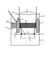
そこで、斜光による混色を防止することができる固体撮像装置として、図12に示すものが存在する。図12は、当該固体撮像装置の断面構造を示した図である。 Therefore, there is a solid-state imaging device shown in FIG. 12 that can prevent color mixture due to oblique light. FIG. 12 is a diagram illustrating a cross-sectional structure of the solid-state imaging device.
図12に示す固体撮像装置は、図11の固体撮像装置に対して、黒色フィルタ110a、bおよびcが、防染膜111aおよびbを介して設けられたものである。このように、黒色フィルタ110a、bおよびcが新たに設けられることにより、図12に示すように、斜光γが当該黒色フィルタ110a、bおよびcで遮光されるようになる。その結果、入射光は、隣接画素の開口部104に対応して形成されたカラーフィルタ106をかすめることなくフォトダイオード102に入射するようになる。これにより、固体撮像装置における混色の問題が低減される。(特許文献1参照)。
しかしながら、図12に示す固体撮像装置では、大きな角度を持った斜め光が入射した場合に、混色が生じるという問題が存在する。以下に詳しく説明する。 However, the solid-state imaging device shown in FIG. 12 has a problem that color mixing occurs when oblique light having a large angle is incident. This will be described in detail below.
図12に示す固体撮像装置では、黒色フィルタ110は、三層構造を有している。そのため、上下方向に隣接する黒色フィルタ110同士の間には、図12に示すように隙間が存在する。そのため、半導体基板101の主面の法線に対して大きな角度をもって入射してきた斜光δは、図12に示すように、黒色フィルタ110同士の間の隙間を通過してしまう。その結果、斜光δは、隣接画素上に形成された別色のカラーフィルタ106を透過した後に入射したり、いずれのカラーフィルタをも経由せずに直接フォトダイオードに入射したりしてしまう。すなわち、混色が発生してしまう。なお、防染膜111の膜厚が充分薄いことおよび黒色フィルタ110の幅が充分太いことの条件を満たすことができない場合には、特に顕著に混色の不具合が発生してしまう。
In the solid-state imaging device shown in FIG. 12, the black filter 110 has a three-layer structure. Therefore, a gap exists between the black filters 110 adjacent in the vertical direction as shown in FIG. Therefore, the oblique light δ incident at a large angle with respect to the normal line of the main surface of the
そこで、本発明の目的は、斜め光による混色をより効果的に防止することができる固体撮像装置を提供すると共に、当該固体撮像装置を製造するための製造方法を提供することとする。 Therefore, an object of the present invention is to provide a solid-state imaging device that can more effectively prevent color mixing due to oblique light, and to provide a manufacturing method for manufacturing the solid-state imaging device.
本発明に係る固体撮像装置は、半導体基板と、半導体基板の主面上に規定された受光領域において、マトリクス状に形成された複数の受光素子と、受光領域の上層に形成され、各受光素子のそれぞれに対応する複数の開口領域を有する遮光膜と、各開口領域の上層に形成され、入射してくる光の内、所定の色を有する光のみを、対応する開口領域に透過する複数のカラーフィルタと、互いに隣接するカラーフィルタ同士の間を壁面によって仕切る遮光壁とを備えている。遮光壁の壁面は、少なくとも、複数のカラーフィルタの内の、最も下層に位置するカラーフィルタの下層側の主面と、最も上層に位置するカラーフィルタの上層側の主面との間において連続した状態で存在する。 A solid-state imaging device according to the present invention includes a semiconductor substrate, a plurality of light receiving elements formed in a matrix in a light receiving region defined on a main surface of the semiconductor substrate, and a light receiving region formed on an upper layer of the light receiving region. A plurality of light-shielding films having a plurality of opening regions corresponding to each of the plurality of light-receiving films, and a plurality of light-transmitting films that are formed in an upper layer of each opening region and transmit only light having a predetermined color among incident light to the corresponding opening regions. A color filter and a light shielding wall that partitions between adjacent color filters by a wall surface are provided. The wall surface of the light shielding wall is continuous between at least the main surface on the lower layer side of the color filter located on the lowermost layer and the upper surface on the upper layer side of the color filter located on the uppermost layer among the plurality of color filters. Exists in a state.
また、遮光壁の形状は、半導体基板の主面に投影した場合において、格子状の形状を有していてもよい。 Moreover, the shape of the light shielding wall may have a lattice shape when projected onto the main surface of the semiconductor substrate.
また、遮光壁の形状は、半導体基板の主面に投影した場合において、ストライプ状の形状を有していてもよい。 The light shielding wall may have a stripe shape when projected onto the main surface of the semiconductor substrate.
また、遮光壁の形状は、半導体基板の主面に投影した場合において、網目の形状を有していてもよい。 Moreover, the shape of the light shielding wall may have a mesh shape when projected onto the main surface of the semiconductor substrate.
また、遮光壁は、開口領域を挟んで互いに対向するもの同士の中点が、開口領域の中心に対して受光領域の中心方向にずれた状態となるように形成され、開口領域を挟んで互いに対向する遮光壁同士の中点と、当該開口領域の中心とのずれ量は、受光領域の中心からの距離に応じた大きさであってもよい。 In addition, the light shielding walls are formed such that the midpoints of those facing each other across the opening region are shifted in the center direction of the light receiving region with respect to the center of the opening region. The amount of deviation between the midpoint of the opposing light shielding walls and the center of the opening area may be a size corresponding to the distance from the center of the light receiving area.
また、開口領域を挟んで互いに対向する遮光パターン同士の中点と、当該開口領域の中心とのずれ量は、受光領域の中心から離れるに従って大きくなっていてもよい。 Further, the amount of deviation between the midpoint of the light shielding patterns facing each other across the opening area and the center of the opening area may increase as the distance from the center of the light receiving area increases.
また、本発明に係る固体撮像装置は、各カラーフィルタに対応するように、各カラーフィルタの上層に形成される複数のマイクロレンズをさらに備えていてもよい。この場合、遮光壁は、下層から上層にいくにしたがって、壁の厚みが薄くなる構造を有することが望ましい。 The solid-state imaging device according to the present invention may further include a plurality of microlenses formed on the upper layer of each color filter so as to correspond to each color filter. In this case, it is desirable that the light shielding wall has a structure in which the thickness of the wall becomes thinner as it goes from the lower layer to the upper layer.
また、本発明に係る固体撮像装置は、遮光壁が形成された領域の下層であって、かつ、遮光膜の上層の領域に配置される遮光壁をさらに備えていてもよい。 In addition, the solid-state imaging device according to the present invention may further include a light shielding wall disposed in a lower layer of the region where the light shielding wall is formed and in an upper layer region of the light shielding film.
また、遮光壁は、光を吸収する特性を有する材質により形成されていてもよい。 Further, the light shielding wall may be formed of a material having a property of absorbing light.
また、遮光壁は、光を反射する特性を有する材質により形成されていてもよい。 The light shielding wall may be formed of a material having a property of reflecting light.
また、本発明は、固体撮像装置のみならず、当該固体撮像装置の製造方法に対しても向けられている。具体的には、半導体基板上に規定された受光領域において、マトリクス状に複数の受光素子を形成し、各受光素子に対応する開口領域を有する遮光膜を、受光領域の上層に形成し、所定の色を有する光のみを透過する複数のカラーフィルタを、それぞれの開口領域の上層に形成し、複数のカラーフィルタの間および上層に透明膜を形成し、透明膜の上層に、各カラーフィルタの間を仕切る形状の開口領域をもつ保護マスクを形成し、保護マスクを用いて、各カラーフィルタの間の透明膜をエッチング除去して、各カラーフィルタの間を仕切る溝を形成し、溝に対して光を遮蔽する物質を埋めこんで遮光壁を形成するようにしてもよい。 The present invention is directed not only to a solid-state imaging device but also to a method for manufacturing the solid-state imaging device. Specifically, in the light receiving region defined on the semiconductor substrate, a plurality of light receiving elements are formed in a matrix, and a light shielding film having an opening region corresponding to each light receiving element is formed in an upper layer of the light receiving region, A plurality of color filters that transmit only light having the above colors are formed in the upper layer of each opening region, a transparent film is formed between and above the plurality of color filters, and each color filter is formed in the upper layer of the transparent film. A protective mask having an opening area in the shape of partitioning is formed, and the transparent film between the color filters is etched away using the protective mask to form a groove for partitioning between the color filters. The light shielding wall may be formed by embedding a light shielding material.
また、遮光壁を形成する工程では、感光性を有しかつ遮光性を有する樹脂を、透明膜および溝に対して塗布し、溝の中心線からの距離に応じて露光量が変化するマスクパターンを用いて、樹脂に対して露光処理を行い、露光処理により露光された部分の樹脂を現像処理により除去することにより、下層から上層にいくにしたがって壁の厚さが薄くなる遮光壁を形成するようにしてもよい。 Further, in the step of forming the light shielding wall, a mask pattern in which a photosensitive and light shielding resin is applied to the transparent film and the groove, and the exposure amount changes according to the distance from the center line of the groove. Is used to perform exposure processing on the resin, and the resin exposed in the exposure processing is removed by development processing, thereby forming a light-shielding wall whose wall thickness decreases from the lower layer to the upper layer. You may do it.
また、遮光壁を形成する工程では、遮光性を有する樹脂を、透明膜および溝に対して塗布し、溝からはみ出した遮光性を有する樹脂をエッチバック法により除去するようにしてもよい。 Further, in the step of forming the light shielding wall, a light shielding resin may be applied to the transparent film and the groove, and the light shielding resin protruding from the groove may be removed by an etch back method.
本発明によれば、遮光壁の壁面は、少なくとも、複数のカラーフィルタの内の、最も下層に位置するカラーフィルタの下層側の主面と、最も上層に位置するカラーフィルタの上層側の主面との間において連続した状態で存在している。その結果、当該遮光壁の隙間から斜光が入ることが防止される。 According to the present invention, the light blocking wall includes at least a main surface on the lower layer side of the color filter located in the lowermost layer and a main surface on the upper layer side of the color filter located in the uppermost layer among the plurality of color filters. Exists in a continuous state. As a result, oblique light is prevented from entering through the gap between the light shielding walls.
また、遮光壁は、開口領域を挟んで互いに対向するもの同士の中点が、開口領域の中心に対して受光領域の中心方向にずれた状態となるように形成される。そして、開口領域を挟んで互いに対向する遮光壁同士の中点と、当該開口領域の中心とのずれ量は、受光領域の中心からの距離に応じた大きさである。そのため、受光領域の中心部と、中心部以外の周辺領域との受光感度の差を小さくすることができる。 The light shielding walls are formed such that the midpoints of the light shielding walls facing each other across the opening region are shifted in the center direction of the light receiving region with respect to the center of the opening region. The amount of deviation between the midpoint of the light shielding walls facing each other across the opening area and the center of the opening area is a size corresponding to the distance from the center of the light receiving area. Therefore, the difference in light receiving sensitivity between the central portion of the light receiving region and the peripheral region other than the central portion can be reduced.
また、本発明によれば、遮光壁は、下層から上層にいくにしたがって、壁の厚みが薄くなる構造を有するので、マイクロレンズを透過した光がより効率的に受光素子に集められる。 In addition, according to the present invention, the light shielding wall has a structure in which the thickness of the wall decreases as it goes from the lower layer to the upper layer, so that the light transmitted through the microlens is more efficiently collected in the light receiving element.
また、本発明によれば、遮光壁が形成された領域の下層であって、かつ、遮光膜の上層の領域に新たな遮光壁が配置される。これにより、斜光が受光素子に入射することがより効果的に防止される。 Further, according to the present invention, a new light shielding wall is disposed in a lower layer of the region where the light shielding wall is formed and in an upper layer region of the light shielding film. This more effectively prevents oblique light from entering the light receiving element.
また、本発明に係る固体撮像装置の製造方法によれば、本発明に係る固体撮像装置を製造することが可能となる。 Moreover, according to the method for manufacturing a solid-state imaging device according to the present invention, the solid-state imaging device according to the present invention can be manufactured.
(第1の実施形態)
以下に、本発明の一実施形態に係る固体撮像装置について、図面を参照しながら説明する。ここで、図1は、本実施形態に係る固体撮像装置の断面構造を示した図である。
(First embodiment)
A solid-state imaging device according to an embodiment of the present invention will be described below with reference to the drawings. Here, FIG. 1 is a diagram showing a cross-sectional structure of the solid-state imaging device according to the present embodiment.
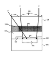
図1に示すように、本実施形態に係る固体撮像装置の画素は、半導体基板1、フォトダイオード2、遮光膜3、開口部4、透明膜5、カラーフィルタ6、遮光壁7、平坦化膜8およびオンチップマイクロレンズ9を備える。本実施形態に係る固体撮像装置は、カラーフィルタ6の下面から上面へと貫通する遮光壁7が設けられることにより、図1に示すような隣の画素から斜めに入射してくる光β(以下、斜光と称す)がフォトダイオード2に入射することを防止している。
As shown in FIG. 1, the pixel of the solid-state imaging device according to the present embodiment includes a
半導体基板1に規定される受光領域には、複数のフォトダイオード2が等間隔にマトリクス状に形成されている。なお、当該フォトダイオード2は、図1の上方から入射してくる光αのうちフォトダイオード2に到達する強度に応じた電荷量を有する信号電荷を発生する。また、複数のフォトダイオード2の間を覆うように遮光膜7が形成されている。当該遮光膜7は、フォトダイオード2とフォトダイオード2との間に光が入射することを防止するための膜である。遮光膜7の一部には、開口部4が形成されている。当該開口部4は、フォトダイオード2に光を入射させるために形成されているものであり、各フォトダイオード2の真上にマトリクス状に等間隔に形成されている。
In the light receiving region defined on the
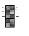
また、遮光膜3および開口部4の上層には、透明膜5が形成される。当該透明膜5は、電気絶縁性を有し、例えば、CVD法により成膜されるBPSG膜、または、塗布により成膜される樹脂膜により形成されている。半導体基板1の主面に対して上方から見たときに開口部4が形成された領域と一致する領域であって、かつ、透明膜5の上層には、カラーフィルタ6が形成されている。当該カラーフィルタ6は、所定の配列で各フォトダイオード2に対応させるように配置させて、マトリクス状に形成されている。ここで、図2は、カラーフィルタ6の配列の一例を示した図である。なお、当該図2は、固体撮像装置を半導体基板1の主面に対して上方から見たときの図である。
A
図2に示すように、カラーフィルタ6は、入射してくる光のうち、特定の色の光のみをフォトダイオード4へと透過し、カラーフィルタ6a、カラーフィルタ6bおよびカラーフィルタ6cが存在する。3種類のカラーフィルタ6としては、例えば、Greenの光を透過するものとRedの光を透過するものとBlueの光を透過するものとが挙げられる。例えば、カラーフィルタ6aがGreenのカラーフィルタとなり、カラーフィルタ6bがRedのカラーフィルタとなり、カラーフィルタ6cがBlueのカラーフィルタとなる。
As shown in FIG. 2, the color filter 6 transmits only light of a specific color from the incident light to the photodiode 4, and there are a
カラーフィルタ6bは、1つの列の中において1行おきに形成される。同様に、カラーフィルタ6cも、1つの列の中において1行おきに形成される。カラーフィルタ6bが形成された列と、カラーフィルタ6cが形成された列とは、交互に配置される。なお、カラーフィルタ6bとカラーフィルタ6cとは、互いに接しないように1行ずらせた状態で形成される。そして、カラーフィルタ6bおよびカラーフィルタ6cが形成されていない部分には、カラーフィルタ6aが形成される。すなわち、カラーフィルタ6aは、いわゆる市松状に形成される。
The
遮光壁7は、遮光性を有する材質で形成され、図1の斜光βがフォトダイオード4に入射して生じる混色を防止する役割を果たす。当該遮光壁7は、互いに隣接するカラーフィルタ6同士の間を壁面によって仕切るように、遮光膜3の上層に形成される。なお、遮光壁7の壁面(図1では、遮光壁7の側面)は、少なくとも、カラーフィルタ6の下層側の主面と上層側の主面との間において、連続した状態で存在する必要がある。これにより、斜光がフォトダイオード4に入射することを有効に防止できる。なお、図1のように全てのカラーフィルタ6が同一の平面に形成されるのではなく、図12に示すように、カラーフィルタが複数の層に存在する場合がある。この場合には、遮光壁7は、複数のカラーフィルタ6の内の、最も下層に位置するカラーフィルタの下層側の主面と、最も上層に位置するカラーフィルタの上層側の主面との間において連続した状態で存在しなければならない。
The
カラーフィルタ6および遮光壁7の上層には、光透過性を有する平坦化膜8が形成される。当該平坦化膜8の上層には、各フォトダイオード2に対応させて、オンチップマイクロレンズ9がマトリクス状に形成されている。当該オンチップマイクロレンズ9は、上方から入射してくる光αをフォトダイオード2に集光する。
On the upper layer of the color filter 6 and the
以上のように、本実施形態に係る固体撮像装置によれば、図1に示すような構造を有することにより、従来の固体撮像装置よりもより有効に混色を防止することができる。以下に、図1を参照しながら説明する。 As described above, according to the solid-state imaging device according to the present embodiment, color mixing can be prevented more effectively than the conventional solid-state imaging device by having the structure shown in FIG. This will be described below with reference to FIG.
図12に示す従来の固体撮像装置では、黒色フィルタ110が多層構造を取っている。そのため、垂直方向に隣接する黒色フィルタ110同士の間には、防染膜111による隙間が存在する。したがって、図12に示すように、半導体基板101の主面の法線に対して大きな角度を持った斜光δが入射してきた場合には、混色が発生してしまうという問題があった。
In the conventional solid-state imaging device shown in FIG. 12, the black filter 110 has a multilayer structure. Therefore, there is a gap due to the stain-proof film 111 between the black filters 110 adjacent in the vertical direction. Therefore, as shown in FIG. 12, when oblique light δ having a large angle with respect to the normal line of the main surface of the
これに対して、本実施形態に係る固体撮像装置は、図1に示すように、遮光壁7がカラーフィルタ6の上面と下面との間において途切れることなく配置されている。そのため、図12において存在していた防染膜111による隙間が存在しない。その結果、半導体基板101の主面に対して大きな角度を持った斜光βは、遮光壁7によりさえぎられてしまう。すなわち、本実施形態に係る固体撮像装置は、従来の固体撮像装置に比べて、より効果的に混色を防止できる。
In contrast, in the solid-state imaging device according to the present embodiment, the
なお、本実施形態に係る固体撮像装置では、図1に示すように、遮光壁7は、長方形の断面構造を有していたが、当該遮光壁7の構造はこれに限らない。当該遮光壁7は、例えば、図3や図4に示すような断面構造であってもよい。具体的には、図3および図4に示す遮光壁7は、上層方向の端部近傍における壁の厚さが下層から上層に行くにしたがって薄くなる形状を有している。これにより、固体撮像装置は、混色を防止しつつ、オンチップマイクロレンズ9を透過した光を効率よくフォトダイオードに集めることができる。
In the solid-state imaging device according to the present embodiment, as shown in FIG. 1, the
また、図5に示すように、本実施形態に係る固体撮像装置において、遮光壁7に加えて、遮光壁10が設けられてもよい。具体的には、遮光壁7の下層の領域であって、かつ遮光膜3の上層の領域に、新たな遮光壁10が設けられてもよい。これにより、より効果的に混色が防止される。
As shown in FIG. 5, in the solid-state imaging device according to the present embodiment, a
(第2の実施形態)
以下に、本発明の第2の実施形態に係る固体撮像装置について図面を参照しながら説明する。第1の実施形態に係る固体撮像装置では、受光領域の全てにわたって図1に示す構造の画素が形成されているのに対して、本実施形態に係る固体撮像装置では、受光領域内の位置により画素の構造が異なる。ここで、図6は、本実施形態に係る固体撮像装置の断面構造を示した図である。具体的には、図6(a)は、受光領域の左端近傍における固体撮像装置の断面構造を示した図である。図6(b)は、受光領域の中央近傍における固体撮像装置の断面構造を示した図である。図6(c)は、受光領域の右端近傍における固体撮像装置の断面構造を示した図である。
(Second Embodiment)
A solid-state imaging device according to the second embodiment of the present invention will be described below with reference to the drawings. In the solid-state imaging device according to the first embodiment, the pixels having the structure shown in FIG. 1 are formed over the entire light receiving region, whereas in the solid-state imaging device according to the present embodiment, depending on the position in the light receiving region. The pixel structure is different. Here, FIG. 6 is a diagram illustrating a cross-sectional structure of the solid-state imaging device according to the present embodiment. Specifically, FIG. 6A is a diagram illustrating a cross-sectional structure of the solid-state imaging device in the vicinity of the left end of the light receiving region. FIG. 6B is a diagram illustrating a cross-sectional structure of the solid-state imaging device in the vicinity of the center of the light receiving region. FIG. 6C is a diagram illustrating a cross-sectional structure of the solid-state imaging device in the vicinity of the right end of the light receiving region.
本実施形態に係る固体撮像装置は、半導体基板1、フォトダイオード2、遮光膜3、開口部4、透明膜5、カラーフィルタ6、遮光壁7、平坦化膜8およびオンチップマイクロレンズ9を備える。なお、これら全ての構成要素の役割は、第1の実施形態と同様であるので説明を省略する。また、半導体基板1、フォトダイオード2、遮光膜3、透明膜5、カラーフィルタ6および平坦化膜8の位置関係も、第1の実施形態と同様であるので説明を省略する。
The solid-state imaging device according to this embodiment includes a
以下に、本実施形態と第1の実施形態との相違点である開口部4と遮光壁7とオンチップマイクロレンズ9との位置関係について図6を参照しながら説明する。
Hereinafter, the positional relationship among the opening 4, the
本実施形態に係る固体撮像装置の遮光壁7は、開口部4を挟んで対向するもの同士の中点が、開口部4の中心に対して受光領域の中心方向にずれた状態となるように形成される。具体的には、受光領域の左端の画素では、図3の(a)のように、遮光壁7は、図1に示す遮光壁7に比べて右方向にずれた状態となるように配置される。また、受光領域の右端の画素では、図3の(c)のように、遮光壁7は、図1に示す遮光壁7に比べて左方向にずれた状態となるように配置される。なお、受光領域の中央の画素は、図1と同様の構成をとる。
As for the
また、受光領域の上端の画素では、遮光壁7は、図1の遮光壁7に比べて下方向にずれた状態となるように配置される(図示せず)。受光領域の下端の画素では、遮光壁7は、図1の遮光壁7に比べて上方向にずれた状態となるように配置される(図示せず)。
Further, in the pixel at the upper end of the light receiving region, the
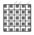
ここで、遮光壁7のずれの大きさについて図7を用いて説明する。図7は、開口部4と遮光壁7との位置関係を示した図である。なお、説明の簡略化のため、受光領域は、5画素×5画素のマトリクス構造としている。
Here, the magnitude | size of the shift | offset | difference of the light-shielding
図7に示すように、開口部4は、遮光膜3に等間隔にマトリクス状に形成されている。さらに、当該遮光膜3の上層には、遮光壁7が形成される。そして、開口部4を挟んで互いに対向する遮光壁7同士の中点と、当該開口部4の中心とのずれ量は、前記受光領域の中心から離れるにしたがって大きくなっている。なお、図7中の黒い丸は、互いに対向する遮光壁7同士の中点を示した点である。また、図7中の黒い四角は、開口部4の中心を示した点である。このように、画素の端にいくにつれて中心方向に遮光壁7をずらして配置することにより、受光領域の中心から離れた位置において入射する光をフォトダイオード2に効率的に集めることができるようになる。
As shown in FIG. 7, the openings 4 are formed in the
以上のように、本実施形態に係る固体撮像装置によれば、第1の実施形態に係る固体撮像装置と同様に斜光がフォトダイオード2に入射することを防止できると共に、受光領域内における画素間の受光感度のばらつきを抑制することができる。
As described above, according to the solid-state imaging device according to the present embodiment, it is possible to prevent oblique light from entering the
なお、本実施形態に係る固体撮像装置では、遮光壁7のずれ量は、受光領域の中心から離れるにしたがって大きくなるものとしているが、当該遮光壁7のずれ量はこれに限らない。例えば、本発明に係る固体撮像装置は、受光領域の中心部から所定距離内に存在する遮光壁7については、ずれ量がなく、かつ受光領域の中心部から所定距離より離れた場所に存在する遮光壁7については、受光領域の中心からの距離に応じたずれ量があるものであってもよい。
In the solid-state imaging device according to the present embodiment, the amount of deviation of the
なお、第1および第2の実施形態において、遮光壁7は、半導体基板1を上方から見たときに、格子状またはストライプ状または網目状となるように形成されることが望ましい。
In the first and second embodiments, it is desirable that the
また、第1および第2の実施形態に係る固体撮像装置では、遮光壁7は、光を透過しない材質により形成されていればよい。したがって、当該材質は、光を吸収する特性を有するものであってもよいし、光を反射する特性を有するものであってもよい。また、当該材質は、これら両方の性質を有するものであってもよい。なお、光を吸収する特性を有する材質としては、例えば黒色を有する樹脂、黒色を有する無機膜、黒色を有する金属または黒色粒体を一定以上の割合で含有する樹脂が挙げられる。また、光を反射する特性を有する材質としては、例えば金属、金属粒体を一定以上の割合で含有する樹脂または金属粒体を一定以上の割合で含有する無機膜が挙げられる。また、光を吸収および反射する両方の特性を有する材質としては、例えば金属粒体を一定以上の割合で含有する黒色の樹脂または金属粒体を一定以上の割合で含有する黒色の無機膜が挙げられる。
Moreover, in the solid-state imaging device according to the first and second embodiments, the
また、第1および第2の実施形態では、カラーフィルタ6が透過する光の色は、Green、RedおよびBlueであるとしたが、カラーフィルタが透過する光の色はこれに限らない。例えば、カラーフィルタ6が透過する光の色は、Cyan、Yellow、Magenta、GreenおよびWhiteなどであってもよい。 In the first and second embodiments, the color of light transmitted through the color filter 6 is Green, Red, and Blue. However, the color of light transmitted through the color filter is not limited to this. For example, the color of light transmitted through the color filter 6 may be Cyan, Yellow, Magenta, Green, White, or the like.
また、第1および第2の実施形態では、CCD型の固体撮像装置で説明を行ったが、本発明に係る固体撮像装置は、MOS型、AMI型等の増幅型固体撮像装置においても有効あることは言うまでもない。 In the first and second embodiments, the CCD type solid-state imaging device has been described. However, the solid-state imaging device according to the present invention is also effective in amplification type solid-state imaging devices such as a MOS type and an AMI type. Needless to say.
(固体撮像装置の製造方法)
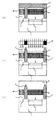
以下に、本発明に係る固体撮像装置の製造方法について図面を参照しながら説明する。なお、ここでは、本発明に係る固体撮像装置の一例として、図3に示す固体撮像装置の製造方法について説明する。図8〜10は、図3に示す固体撮像装置を製造する各過程における当該固体撮像装置の断面構造を示した図である。
(Method for manufacturing solid-state imaging device)
Hereinafter, a method for manufacturing a solid-state imaging device according to the present invention will be described with reference to the drawings. Here, as an example of the solid-state imaging device according to the present invention, a method for manufacturing the solid-state imaging device shown in FIG. 3 will be described. 8 to 10 are diagrams showing a cross-sectional structure of the solid-state imaging device in each process of manufacturing the solid-state imaging device shown in FIG.
まず、図8(a)に示すように、半導体基板1の受光領域に、等間隔にマトリクス状となるようにフォトダイオード2を形成する。次に、図8(b)に示すように、複数の当該フォトダイオード2の間を覆うように遮光性を有する遮光膜3を形成する。具体的には、W(タングステン)の薄膜をPVD法あるいはCVD法により形成する。その後、フォトダイオード2の上部に位置するWの薄膜をドライエッチングにより選択的に除去する。これにより、図8(b)に示すような、遮光膜3が形成されると共に、開口部4が形成される。
First, as shown in FIG. 8A, the
次に、図8(c)に示すように、遮光膜3および開口部4の上層に、透明膜5を形成する。例えば、BPSG膜を用いて透明膜5をCVD法により堆積する。その後、加熱処理によりBPSG膜をリフローして、その表面を平坦化する。これにより、透明膜5が形成される。
Next, as shown in FIG. 8C, a
次に、図8(d)に示すように、透明膜5の上層であって、かつ、開口部4の上の領域に、カラーフィルタ6を形成する。カラーフィルタ6は、所定の配列で各フォトダイオード2に対応させるようにマトリクス状に形成される。カラーフィルタ6は、被染色性パターンを形成した後に染色処理により所望の着色パターンを得る染色法、または、染料または顔料を含有する感光性材料を用いてフォトリソグラフィ法により着色パターンを得るカラーレジスト法等の方法により形成される。
Next, as shown in FIG. 8D, the color filter 6 is formed in the region above the
次に、カラーフィルタ6を形成した後の表面の平坦性を向上させるために、図9(e)に示すように、カラーフィルタ6の上層に、平坦化膜17を形成する。当該平坦化膜17は、例えば透明樹脂材料により形成される。
Next, in order to improve the flatness of the surface after the color filter 6 is formed, a
次に、図9(f)に示すように、カラーフィルタ6のそれぞれの間を仕切る形状の開口領域をもつレジストパターン16を、平坦化膜17上にフォトリソグラフィ法により形成する。
Next, as shown in FIG. 9 (f), a resist
次に、CF系ガスまたは酸素ガスを用いたドライエッチングを行って、当該レジストパターン16を保護マスクとして、レジストパターン16の開口領域の下層に存在する平坦化膜17およびカラーフィルタ6の端部を選択的に除去することにより溝20を形成する。当該ドライエッチング処理では、カラーフィルタ6の下層側の主面に溝20の底部が到達するように、平坦化膜17が除去される。なお、当該溝20は、遮光壁7に求める遮光能力に応じて、その幅を決定することができる。例えば、遮光性を強くする場合には溝20の幅は太く、遮光性が弱くてもよい場合には溝20の幅は細く形成すればよい。この後、図9(g)に示すように、有機溶剤からなるレジスト剥離液を用いてレジストパターンの残留物を除去する。
Next, dry etching using CF-based gas or oxygen gas is performed, and the end portions of the
次に、図10(h)に示すように、遮光性を有する材料を、溝20を埋めるように塗布して、遮光壁用膜18を形成する。なお、遮光壁用膜18に用いられる材料は、遮光性を有すると共に、感光性を有する樹脂であることが望ましい。
Next, as shown in FIG. 10H, a light shielding material is applied so as to fill the groove 20 to form the light shielding
次に、図10(i)に示すように、フォトリソグラフィ法により、遮光壁用膜18の一部を除去して、平坦化膜17を露出させて、上層側の端部近傍における壁の厚さが下層から上層に行くにしたがって細くなる遮光壁7を形成する。具体的には、まず、溝20の中心線からの距離に応じて露光量が変化するマスクパターン19を用いて、露光処理を行う。次に、現像処理を行うことにより、遮光膜用膜18のうち露光された部位を除去する。なお、本実施形態では、溝20の中心からの距離が大きくなるにしたがって、露光量が大きくなるものがマスクパターン19として用いられる。
Next, as shown in FIG. 10I, a part of the light
次に、図10(j)に示すように、平坦化膜17および遮光壁7の上層に、表面の平坦性を向上させるために、例えば平坦化膜17と同じ透明樹脂材料を用いて透明膜を追加形成する。これにより、平坦化膜8が形成される。
Next, as shown in FIG. 10 (j), in order to improve the flatness of the surface on the
最後に、平坦化膜8の上層にオンチップマイクロレンズ8を形成する。具体的には、熱溶融性透明樹脂やその上部のレジスト熱リフロー転写により、オンチップマイクロレンズ8を形成する。以上のような工程を経て、図3に示すような構造を有する固体撮像装置が完成する。
Finally, an on-
なお、本実施形態に係る固体撮像装置では、遮光壁7を形成するにあたって、遮光性を有さない膜を塗布した後にフォトリソグラフィおよび染色法により遮光性を有する黒色パターンを形成してもよい。
In the solid-state imaging device according to the present embodiment, when the
なお、本実施形態に係る固体撮像装置では、遮光壁7を形成するにあたって、黒色を有する樹脂材料または金属粒体を一定以上の割合で含有する樹脂を塗布することにより溝20を埋めた後、エッチバック法またはCMP法により平坦化膜17を露出させる方法によって遮光壁7を形成してもよい。但し、この場合、遮光膜7は、図1のような形状を有する。
In the solid-state imaging device according to the present embodiment, in forming the
なお、遮光壁用膜18から遮光壁7に加工する方法としては、フォトリソグラフィ法により、カラーフィルタ6のそれぞれの間を仕切る形状の開口領域を有するレジストパターンを形成した後、レジストパターンを保護マスクとしてレジストパターンの形成されていない領域下に存在する遮光壁用膜18を、ドライエッチまたはウェットエッチにより選択的に除去することによって形成してもよい。
As a method of processing the light shielding
なお、エッチングする際の異方性および等方性を制御することにより、遮光壁7が鉛直方向に下層から上層方向に向かって壁の厚さが薄くなる構造を有するように加工することが出来る。具体的には、異方性のエッチングにて一定の膜厚の遮光壁用膜18を除去したのち、等方性のエッチングにて平坦化膜17が露出するように残りの遮光壁用膜18を除去することによって形成してもよい。
By controlling the anisotropy and isotropy during etching, the
なお、遮光壁7が、鉛直方向の断面構造が下層から上層方向に向かって壁の厚さ薄くなる構造を有するように加工する場合の例として、遮光壁7を形成した後に再び透明膜を追加形成する製造方法の例を示して説明した。しかしながら、遮光壁7を形成した後の表面の凹凸が、オンチップマイクロレンズ9を形成するための平坦性を充分有する場合には、遮光壁7を形成した後の透明膜の追加形成を省略してもよい。
In addition, as an example in the case where the
なお、遮光膜3上に形成される透明膜5は、絶縁性および光透過性を有する薄膜を形成した後に、当該薄膜に対して平坦化処理が行われて形成されてもよい。なお、絶縁性および光透過性を有する薄膜の形成方法としては、例えば、SOG等の樹脂系塗布をする方法や、TEOS系SiO2/BPSGをCVD法により堆積する方法や、バイアス高密度プラズマ法によるSiO2系の膜を堆積する方法が挙げられる。また、平坦化処理としては、例えば、エッチバックまたはCMP法が挙げられる。また、平坦化膜は、SiO2ではなく、SiONであってもよい。
The
なお、遮光壁用膜18から遮光壁7を加工する方法としては、ポジ型フォトレジストを用いた例を示したが、ネガ型レジストであっても同様の加工を実現することも可能である。
As a method of processing the
また、上記固体撮像装置の製造方法では、図3に示す固体撮像装置の製造方法について説明を行った。ここで、図1に示す固体撮像装置を製造する場合には、図10(i)のフォトリソグラフィ処理が不要である。また、図6に示す第2の実施形態に係る固体撮像装置を製造する場合には、図9(f)において形成さえるレジスタパターン16の開口領域は、遮光膜3に形成された各開口部4を挟んで互いに対向するもの同士の中点が、各開口部4の中心に対して受光領域の中心方向にずれた状態とならなければならない。なお、遮光膜3の各開口部4を挟んで互いに対向するもの同士の中点と、各開口部4の中心とのずれ量は、受光領域の中心から離れるにしたがって大きくなる。また、この場合には、オンチップマイクロレンズ9は、開口部4の中心に対して、遮光壁7のずれ量に応じて、受光領域の中心方向にずれた位置に形成されることが望ましい。
In the method for manufacturing the solid-state imaging device, the method for manufacturing the solid-state imaging device shown in FIG. 3 has been described. Here, when the solid-state imaging device shown in FIG. 1 is manufactured, the photolithography process of FIG. When the solid-state imaging device according to the second embodiment shown in FIG. 6 is manufactured, the opening area of the
本発明に係る固体撮像装置は、斜め光による混色をより防止することができる効果を有し、カラーフィルタを備えた固体撮像装置等として有用である。 The solid-state imaging device according to the present invention has an effect of further preventing color mixing due to oblique light, and is useful as a solid-state imaging device including a color filter.
1 半導体基板
2 フォトダイオード
3 遮光膜
4 開口部
5 透明膜
6 カラーフィルタ
7 遮光壁
8 平坦化膜
9 オンチップマイクロレンズ
10 遮光壁
11 防染膜
16 レジストパターン
17 平坦化膜
18 遮光壁用膜
19 マスクパターン
20 溝
DESCRIPTION OF
Claims (14)
前記半導体基板の主面上に規定された受光領域において、マトリクス状に形成された複数の受光素子と、
前記受光領域の上層に形成され、各前記受光素子のそれぞれに対応する複数の開口領域を有する遮光膜と、
各前記開口領域の上層に形成され、入射してくる光の内、所定の色を有する光のみを、対応する開口領域に透過する複数のカラーフィルタと、
互いに隣接する前記カラーフィルタ同士の間を壁面によって仕切る遮光壁とを備え、
前記遮光壁の壁面は、複数のカラーフィルタの内の、最も下層に位置するカラーフィルタの下層側の主面と、最も上層に位置するカラーフィルタの上層側の主面との間において連続した状態で存在することを特徴とする、固体撮像装置。 A semiconductor substrate;
In the light receiving region defined on the main surface of the semiconductor substrate, a plurality of light receiving elements formed in a matrix, and
A light shielding film formed in an upper layer of the light receiving region and having a plurality of opening regions corresponding to each of the light receiving elements;
A plurality of color filters that are formed in an upper layer of each of the opening regions and transmit only light having a predetermined color among incident light to the corresponding opening regions;
A light shielding wall that partitions the color filters adjacent to each other by a wall surface;
The wall surface of the light shielding wall is a continuous state between the lower principal surface of the color filter located in the lowermost layer and the upper major surface of the color filter located in the uppermost layer among the plurality of color filters. A solid-state imaging device, characterized in that:
前記開口領域を挟んで互いに対向する前記遮光壁同士の中点と、当該開口領域の中心とのずれ量は、前記受光領域の中心からの距離に応じた大きさであることを特徴とする、請求項2に記載の固体撮像装置。 The light shielding wall is formed such that a midpoint between those facing each other across the opening region is shifted in a center direction of the light receiving region with respect to a center of the opening region,
The amount of deviation between the midpoint between the light shielding walls facing each other across the opening region and the center of the opening region is a size according to the distance from the center of the light receiving region, The solid-state imaging device according to claim 2.
前記遮光壁は、下層から上層にいくにしたがって、壁の厚みが薄くなる構造を有することを特徴とする、請求項1に記載の固体撮像装置。 In order to correspond to each of the color filters, further comprising a plurality of microlenses formed in the upper layer of each color filter,
2. The solid-state imaging device according to claim 1, wherein the light shielding wall has a structure in which the thickness of the wall becomes thinner from the lower layer to the upper layer.
各前記受光素子に対応する開口領域を有する遮光膜を、前記受光領域の上層に形成する工程と、
所定の色を有する光のみを透過する複数のカラーフィルタを、それぞれの前記開口領域の上層に形成する工程と、
複数の前記カラーフィルタの間および上層に透明膜を形成する工程と、
前記透明膜の上層に、各前記カラーフィルタの間を仕切る形状の開口領域をもつ保護マスクを形成する工程と、
前記保護マスクを用いて、各前記カラーフィルタの間の透明膜をエッチング除去して、各前記カラーフィルタの間を仕切り、かつ、各当該カラーフィルタのうち最も下層側に置するカラーフィルタの主面よりも底部が下層側に位置する溝を形成する工程と、
前記溝に対して光を遮蔽する物質を埋めこんで遮光壁を形成する工程とを備えた固体撮像装置の製造方法。 Forming a plurality of light receiving elements in a matrix in a light receiving region defined on a semiconductor substrate;
Forming a light shielding film having an opening region corresponding to each of the light receiving elements in an upper layer of the light receiving region;
Forming a plurality of color filters that transmit only light having a predetermined color in an upper layer of each of the opening regions;
Forming a transparent film between and above the plurality of color filters;
Forming a protective mask having an opening region in a shape partitioning the color filters on the transparent film;
Using the protective mask, the transparent film between the color filters is etched away to partition the color filters, and the main surface of the color filter placed on the lowermost side of the color filters Forming a groove whose bottom is positioned on the lower layer side, and
And a step of forming a light shielding wall by embedding a light shielding material in the groove.
感光性を有しかつ遮光性を有する樹脂を、前記透明膜および前記溝に対して塗布する工程と、
前記溝の中心線からの距離に応じて露光量が変化するマスクパターンを用いて、前記樹脂に対して露光処理を行う工程と、
前記露光処理により露光された樹脂の一部を現像処理により除去することにより、下層から上層にいくにしたがって壁の厚さが薄くなる遮光壁を形成する工程とを含む、請求項11に記載の固体撮像装置の製造方法。 The step of forming the light shielding wall includes:
Applying a photosensitive and light-shielding resin to the transparent film and the groove;
A step of performing an exposure process on the resin using a mask pattern in which an exposure amount changes according to a distance from a center line of the groove;
The step of forming a light-shielding wall in which the thickness of the wall decreases as it goes from the lower layer to the upper layer by removing a part of the resin exposed by the exposure process by a development process. Manufacturing method of solid-state imaging device.
遮光性を有する樹脂を、前記透明膜および前記溝に対して塗布する工程と、
前記溝からはみ出した前記遮光性を有する樹脂をエッチバック法により除去する工程とを含む、請求項11に記載の固体撮像装置の製造方法。 The step of forming the light shielding wall includes:
Applying a light-shielding resin to the transparent film and the groove;
The method for manufacturing a solid-state imaging device according to claim 11, further comprising: removing the light-shielding resin protruding from the groove by an etch back method.
遮光性を有する樹脂を、前記透明膜および前記溝に対して塗布する工程と、
前記遮光性を有する樹脂上にレジスト材料を塗布する工程と、
前記溝上にレジストパターンを形成する工程と、
前記レジストパターンを保護マスクとしてエッチングを行うにより前記溝からはみ出した前記遮光性を有する樹脂を除去する工程とを含む、請求項11に記載の固体撮像装置の製造方法。
The step of forming the light shielding wall includes:
Applying a light-shielding resin to the transparent film and the groove;
Applying a resist material on the light-shielding resin;
Forming a resist pattern on the groove;
The method for manufacturing a solid-state imaging device according to claim 11, comprising: removing the light-blocking resin protruding from the groove by etching using the resist pattern as a protective mask.
Priority Applications (1)
| Application Number | Priority Date | Filing Date | Title |
|---|---|---|---|
| JP2004109320A JP2005294647A (en) | 2004-04-01 | 2004-04-01 | Solid state image pickup apparatus and method for manufacturing the same |
Applications Claiming Priority (1)
| Application Number | Priority Date | Filing Date | Title |
|---|---|---|---|
| JP2004109320A JP2005294647A (en) | 2004-04-01 | 2004-04-01 | Solid state image pickup apparatus and method for manufacturing the same |
Publications (2)
| Publication Number | Publication Date |
|---|---|
| JP2005294647A true JP2005294647A (en) | 2005-10-20 |
| JP2005294647A5 JP2005294647A5 (en) | 2007-04-19 |
Family
ID=35327219
Family Applications (1)
| Application Number | Title | Priority Date | Filing Date |
|---|---|---|---|
| JP2004109320A Withdrawn JP2005294647A (en) | 2004-04-01 | 2004-04-01 | Solid state image pickup apparatus and method for manufacturing the same |
Country Status (1)
| Country | Link |
|---|---|
| JP (1) | JP2005294647A (en) |
Cited By (35)
| Publication number | Priority date | Publication date | Assignee | Title |
|---|---|---|---|---|
| JP2008108918A (en) * | 2006-10-25 | 2008-05-08 | Sony Corp | Solid-state imaging element |
| JP2009010219A (en) * | 2007-06-28 | 2009-01-15 | Sony Corp | Solid-state imaging device camera module |
| JP2009021415A (en) * | 2007-07-12 | 2009-01-29 | Panasonic Corp | Solid-state imaging apparatus and manufacturing method thereof |
| JP2009206356A (en) * | 2008-02-28 | 2009-09-10 | Toshiba Corp | Solid-state imaging device and manufacturing method thereof |
| JP2010004018A (en) * | 2008-05-22 | 2010-01-07 | Sony Corp | Solid-state imaging device, manufacturing method thereof and electronic device |
| WO2010010652A1 (en) * | 2008-07-25 | 2010-01-28 | パナソニック株式会社 | Solid state imaging device and method for manufacturing the same |
| WO2010013432A1 (en) * | 2008-07-31 | 2010-02-04 | パナソニック株式会社 | Solid-state imaging device and method for fabricating the same |
| JP2010134353A (en) * | 2008-12-08 | 2010-06-17 | Fujifilm Corp | Method for producing color filter and solid-state imaging apparatus |
| JP2010263228A (en) * | 2008-05-22 | 2010-11-18 | Sony Corp | Solid-state imaging device, manufacturing method thereof, and electronic device |
| CN101997011A (en) * | 2009-08-24 | 2011-03-30 | 株式会社半导体能源研究所 | Photodetector and display device |
| JP2011176715A (en) * | 2010-02-25 | 2011-09-08 | Nikon Corp | Back-illuminated image sensor and imaging apparatus |
| JP2012194055A (en) * | 2011-03-16 | 2012-10-11 | Seiko Epson Corp | Optical sensor and electronic apparatus |
| US20120273906A1 (en) * | 2011-04-28 | 2012-11-01 | Jeffrey Mackey | Dielectric barriers for pixel arrays |
| JP2013156325A (en) * | 2012-01-27 | 2013-08-15 | Seiko Epson Corp | Spectroscopic sensor and angle limit filter |
| JP2014033107A (en) * | 2012-08-03 | 2014-02-20 | Sony Corp | Solid-state imaging device, method of manufacturing the same, and electronic apparatus |
| JP2014082310A (en) * | 2012-10-16 | 2014-05-08 | Canon Inc | Solid state image pickup device, method for manufacturing solid state image pickup divide, and image pickup system |
| WO2015019913A1 (en) * | 2013-08-07 | 2015-02-12 | ソニー株式会社 | Solid-state imaging device and electronic device |
| JP2015092521A (en) * | 2013-11-08 | 2015-05-14 | ルネサスエレクトロニクス株式会社 | Semiconductor device and manufacturing method of the same |
| JP2017011207A (en) * | 2015-06-25 | 2017-01-12 | 三重富士通セミコンダクター株式会社 | Solid state image pickup device and shielding method |
| US9709715B2 (en) | 2011-03-17 | 2017-07-18 | Seiko Epson Corporation | Spectroscopic sensor and angle limiting filter |
| JP2018133575A (en) * | 2018-03-08 | 2018-08-23 | ソニー株式会社 | Solid-state imaging device, electronic device, and manufacturing method of solid-state imaging device |
| WO2019093135A1 (en) * | 2017-11-08 | 2019-05-16 | ソニーセミコンダクタソリューションズ株式会社 | Image capture element, method of manufacturing same, and electronic apparatus |
| CN109841652A (en) * | 2017-11-28 | 2019-06-04 | 乐金显示有限公司 | Display device with light-emitting component and colour filter |
| US10446611B2 (en) | 2018-02-12 | 2019-10-15 | Samsung Electronics Co., Ltd. | Image sensor including color filters separated by two insulating layers and method of manufacturing the same |
| US10490586B2 (en) | 2014-10-03 | 2019-11-26 | Sony Semiconductor Solutions Corporation | Solid-state imaging device with light shielding films, method of manufacturing the same, and electronic apparatus |
| JP2020065040A (en) * | 2018-10-17 | 2020-04-23 | キヤノン株式会社 | Photoelectric conversion device and apparatus |
| CN111063701A (en) * | 2018-10-17 | 2020-04-24 | 佳能株式会社 | Photoelectric conversion device and equipment including photoelectric conversion device |
| FR3087939A1 (en) * | 2018-10-30 | 2020-05-01 | Stmicroelectronics (Grenoble 2) Sas | LIGHT SENSOR |
| WO2020137285A1 (en) * | 2018-12-27 | 2020-07-02 | ソニーセミコンダクタソリューションズ株式会社 | Imaging element and method for manufacturing imaging element |
| JP2020145397A (en) * | 2018-10-17 | 2020-09-10 | キヤノン株式会社 | Photoelectric conversion apparatus and equipment including the same |
| JP2020167435A (en) * | 2015-01-13 | 2020-10-08 | ソニーセミコンダクタソリューションズ株式会社 | Solid-state imaging element and electronic apparatus |
| WO2021100298A1 (en) * | 2019-11-21 | 2021-05-27 | ソニーセミコンダクタソリューションズ株式会社 | Imaging element and imaging device |
| US11121160B2 (en) | 2018-10-17 | 2021-09-14 | Canon Kabushiki Kaisha | Photoelectric conversion apparatus and equipment comprising a light shielding part in a light receiving region and a light shielding film in a light shielded region |
| JP2022014884A (en) * | 2020-07-07 | 2022-01-20 | 采▲ぎょく▼科技股▲ふん▼有限公司 | Image sensor |
| WO2023068172A1 (en) * | 2021-10-20 | 2023-04-27 | ソニーセミコンダクタソリューションズ株式会社 | Imaging device |
-
2004
- 2004-04-01 JP JP2004109320A patent/JP2005294647A/en not_active Withdrawn
Cited By (70)
| Publication number | Priority date | Publication date | Assignee | Title |
|---|---|---|---|---|
| JP2008108918A (en) * | 2006-10-25 | 2008-05-08 | Sony Corp | Solid-state imaging element |
| US9257477B2 (en) | 2007-06-28 | 2016-02-09 | Sony Corporation | Solid-state imaging device and camera module |
| JP2009010219A (en) * | 2007-06-28 | 2009-01-15 | Sony Corp | Solid-state imaging device camera module |
| US8648943B2 (en) | 2007-06-28 | 2014-02-11 | Sony Corporation | Solid-state imaging device and camera module |
| US9640578B2 (en) | 2007-06-28 | 2017-05-02 | Sony Corporation | Solid-state imaging device and camera module |
| JP2009021415A (en) * | 2007-07-12 | 2009-01-29 | Panasonic Corp | Solid-state imaging apparatus and manufacturing method thereof |
| JP2009206356A (en) * | 2008-02-28 | 2009-09-10 | Toshiba Corp | Solid-state imaging device and manufacturing method thereof |
| US8823847B2 (en) | 2008-02-28 | 2014-09-02 | Kabushiki Kaisha Toshiba | Solid-state imaging device and manufacturing method thereof |
| US8390707B2 (en) | 2008-02-28 | 2013-03-05 | Kabushiki Kaisha Toshiba | Solid-state imaging device and manufacturing method thereof |
| JP2010263228A (en) * | 2008-05-22 | 2010-11-18 | Sony Corp | Solid-state imaging device, manufacturing method thereof, and electronic device |
| JP2010004018A (en) * | 2008-05-22 | 2010-01-07 | Sony Corp | Solid-state imaging device, manufacturing method thereof and electronic device |
| US8373786B2 (en) | 2008-05-22 | 2013-02-12 | Sony Corporation | Solid-state imaging device, manufacturing method thereof, and electronic device |
| WO2010010652A1 (en) * | 2008-07-25 | 2010-01-28 | パナソニック株式会社 | Solid state imaging device and method for manufacturing the same |
| JP2010034426A (en) * | 2008-07-31 | 2010-02-12 | Panasonic Corp | Solid-state imaging device, method of manufacturing the same, and camera |
| WO2010013432A1 (en) * | 2008-07-31 | 2010-02-04 | パナソニック株式会社 | Solid-state imaging device and method for fabricating the same |
| JP2010134353A (en) * | 2008-12-08 | 2010-06-17 | Fujifilm Corp | Method for producing color filter and solid-state imaging apparatus |
| CN101997011A (en) * | 2009-08-24 | 2011-03-30 | 株式会社半导体能源研究所 | Photodetector and display device |
| US11979672B2 (en) | 2010-02-25 | 2024-05-07 | Nikon Corporation | Backside illumination image sensor and image-capturing device |
| US9466633B2 (en) | 2010-02-25 | 2016-10-11 | Nikon Corporation | Backside illumination image sensor and image-capturing device |
| US11601624B2 (en) | 2010-02-25 | 2023-03-07 | Nikon Corporation | Backside illumination image sensor and image-capturing device |
| JP2011176715A (en) * | 2010-02-25 | 2011-09-08 | Nikon Corp | Back-illuminated image sensor and imaging apparatus |
| US8928795B2 (en) | 2010-02-25 | 2015-01-06 | Nikon Corporation | Backside illumination image sensor and image-capturing device |
| US10777595B2 (en) | 2010-02-25 | 2020-09-15 | Nikon Corporation | Backside illumination image sensor and image-capturing device |
| US10204949B2 (en) | 2010-02-25 | 2019-02-12 | Nikon Corporation | Backside illumination image sensor and image-capturing device |
| US9704902B2 (en) | 2010-02-25 | 2017-07-11 | Nikon Corporation | Backside illumination image sensor and image-capturing device |
| US9184197B2 (en) | 2010-02-25 | 2015-11-10 | Nikon Corporation | Backside illumination image sensor and image-capturing device |
| JP2012194055A (en) * | 2011-03-16 | 2012-10-11 | Seiko Epson Corp | Optical sensor and electronic apparatus |
| US9709715B2 (en) | 2011-03-17 | 2017-07-18 | Seiko Epson Corporation | Spectroscopic sensor and angle limiting filter |
| TWI548072B (en) * | 2011-04-28 | 2016-09-01 | 普廷數碼影像控股公司 | Dielectric barriers for pixel arrays |
| US20120273906A1 (en) * | 2011-04-28 | 2012-11-01 | Jeffrey Mackey | Dielectric barriers for pixel arrays |
| US9093579B2 (en) * | 2011-04-28 | 2015-07-28 | Semiconductor Components Industries, Llc | Dielectric barriers for pixel arrays |
| JP2013156325A (en) * | 2012-01-27 | 2013-08-15 | Seiko Epson Corp | Spectroscopic sensor and angle limit filter |
| US9748296B2 (en) | 2012-08-03 | 2017-08-29 | Sony Corporation | Solid-state imaging device, method for producing solid-state imaging device and electronic apparatus |
| JP2014033107A (en) * | 2012-08-03 | 2014-02-20 | Sony Corp | Solid-state imaging device, method of manufacturing the same, and electronic apparatus |
| JP2014082310A (en) * | 2012-10-16 | 2014-05-08 | Canon Inc | Solid state image pickup device, method for manufacturing solid state image pickup divide, and image pickup system |
| US9595551B2 (en) | 2013-08-07 | 2017-03-14 | Sony Corporation | Solid-state imaging device and electronic apparatus |
| WO2015019913A1 (en) * | 2013-08-07 | 2015-02-12 | ソニー株式会社 | Solid-state imaging device and electronic device |
| JPWO2015019913A1 (en) * | 2013-08-07 | 2017-03-02 | ソニー株式会社 | Solid-state imaging device and electronic apparatus |
| KR20160040459A (en) * | 2013-08-07 | 2016-04-14 | 소니 주식회사 | Solid-state imaging device and electronic device |
| KR102223515B1 (en) | 2013-08-07 | 2021-03-04 | 소니 주식회사 | Solid-state imaging device and electronic device |
| JP2015092521A (en) * | 2013-11-08 | 2015-05-14 | ルネサスエレクトロニクス株式会社 | Semiconductor device and manufacturing method of the same |
| US10490586B2 (en) | 2014-10-03 | 2019-11-26 | Sony Semiconductor Solutions Corporation | Solid-state imaging device with light shielding films, method of manufacturing the same, and electronic apparatus |
| JP2020167435A (en) * | 2015-01-13 | 2020-10-08 | ソニーセミコンダクタソリューションズ株式会社 | Solid-state imaging element and electronic apparatus |
| JP7171652B2 (en) | 2015-01-13 | 2022-11-15 | ソニーセミコンダクタソリューションズ株式会社 | Solid-state image sensor and electronic equipment |
| US11482561B2 (en) | 2015-01-13 | 2022-10-25 | Sony Semiconductor Solutions Corporation | Solid-state imaging device, manufacturing method thereof, and electronic apparatus |
| JP2017011207A (en) * | 2015-06-25 | 2017-01-12 | 三重富士通セミコンダクター株式会社 | Solid state image pickup device and shielding method |
| WO2019093135A1 (en) * | 2017-11-08 | 2019-05-16 | ソニーセミコンダクタソリューションズ株式会社 | Image capture element, method of manufacturing same, and electronic apparatus |
| CN109841652A (en) * | 2017-11-28 | 2019-06-04 | 乐金显示有限公司 | Display device with light-emitting component and colour filter |
| CN109841652B (en) * | 2017-11-28 | 2023-06-23 | 乐金显示有限公司 | Display device having light emitting element and color filter |
| US10446611B2 (en) | 2018-02-12 | 2019-10-15 | Samsung Electronics Co., Ltd. | Image sensor including color filters separated by two insulating layers and method of manufacturing the same |
| US10784314B2 (en) | 2018-02-12 | 2020-09-22 | Samsung Electronics Co., Ltd. | Image sensor including color filters |
| JP2018133575A (en) * | 2018-03-08 | 2018-08-23 | ソニー株式会社 | Solid-state imaging device, electronic device, and manufacturing method of solid-state imaging device |
| JP2022051782A (en) * | 2018-10-17 | 2022-04-01 | キヤノン株式会社 | Photoelectric conversion apparatus and equipment including the same |
| JP2020065040A (en) * | 2018-10-17 | 2020-04-23 | キヤノン株式会社 | Photoelectric conversion device and apparatus |
| US11682686B2 (en) | 2018-10-17 | 2023-06-20 | Canon Kabushiki Kaisha | Photoelectric conversion apparatus and equipment including the same |
| US11121160B2 (en) | 2018-10-17 | 2021-09-14 | Canon Kabushiki Kaisha | Photoelectric conversion apparatus and equipment comprising a light shielding part in a light receiving region and a light shielding film in a light shielded region |
| JP2020145397A (en) * | 2018-10-17 | 2020-09-10 | キヤノン株式会社 | Photoelectric conversion apparatus and equipment including the same |
| CN111063701A (en) * | 2018-10-17 | 2020-04-24 | 佳能株式会社 | Photoelectric conversion device and equipment including photoelectric conversion device |
| JP7008054B2 (en) | 2018-10-17 | 2022-01-25 | キヤノン株式会社 | Photoelectric converters and equipment |
| US11244978B2 (en) | 2018-10-17 | 2022-02-08 | Canon Kabushiki Kaisha | Photoelectric conversion apparatus and equipment including the same |
| FR3087939A1 (en) * | 2018-10-30 | 2020-05-01 | Stmicroelectronics (Grenoble 2) Sas | LIGHT SENSOR |
| US10998455B2 (en) | 2018-10-30 | 2021-05-04 | Stmicroelectronics (Grenoble 2) Sas | Light sensor |
| WO2020137285A1 (en) * | 2018-12-27 | 2020-07-02 | ソニーセミコンダクタソリューションズ株式会社 | Imaging element and method for manufacturing imaging element |
| JP7544602B2 (en) | 2018-12-27 | 2024-09-03 | ソニーセミコンダクタソリューションズ株式会社 | Image sensor |
| JPWO2020137285A1 (en) * | 2018-12-27 | 2021-11-11 | ソニーセミコンダクタソリューションズ株式会社 | Image sensor and manufacturing method of image sensor |
| CN113169200A (en) * | 2018-12-27 | 2021-07-23 | 索尼半导体解决方案公司 | Imaging element and method for manufacturing imaging element |
| WO2021100298A1 (en) * | 2019-11-21 | 2021-05-27 | ソニーセミコンダクタソリューションズ株式会社 | Imaging element and imaging device |
| JP2022014884A (en) * | 2020-07-07 | 2022-01-20 | 采▲ぎょく▼科技股▲ふん▼有限公司 | Image sensor |
| JP7270679B2 (en) | 2020-07-07 | 2023-05-10 | 采▲ぎょく▼科技股▲ふん▼有限公司 | image sensor |
| WO2023068172A1 (en) * | 2021-10-20 | 2023-04-27 | ソニーセミコンダクタソリューションズ株式会社 | Imaging device |
Similar Documents
| Publication | Publication Date | Title |
|---|---|---|
| JP2005294647A (en) | Solid state image pickup apparatus and method for manufacturing the same | |
| US8139131B2 (en) | Solid state imaging device and fabrication method thereof, and camera incorporating the solid state imaging device | |
| JP4598680B2 (en) | Solid-state imaging device and camera | |
| WO2013121742A1 (en) | Image pickup element | |
| US7777794B2 (en) | Solid-state imaging device and method of manufacturing the same | |
| US20100253819A1 (en) | Solid state imaging device and method for manufacturing the same | |
| JP2007219515A (en) | Color filter, color filter array, method of manufacturing color filter array, and image sensor | |
| US7777795B2 (en) | Solid-state image pickup device | |
| JP2005340299A (en) | Solid-state image pickup device, its manufacturing method and camera | |
| JP2011171328A (en) | Solid-state image pickup element and method of manufacturing the same | |
| JP2010062417A (en) | Solid-state imaging device and method of manufacturing the same | |
| KR100868630B1 (en) | Pattern mask used for forming micro lense, image sensor and method of manufacturing the same | |
| US8664680B2 (en) | Color filter structure and method for fabricating the same | |
| JP4905760B2 (en) | Color filter manufacturing method, color filter, solid-state image sensor manufacturing method, and solid-state image sensor using the same | |
| JP2006003869A (en) | Method for forming microlenses of image sensor | |
| JP2006186203A (en) | Solid-state image pick-up device, manufacturing method therefor, and camera | |
| JP2000260968A (en) | Solid-state image pickup element and its manufacture | |
| JP2009152314A (en) | Image sensor and its manufacturing method | |
| JP4696385B2 (en) | Manufacturing method of color solid-state imaging device | |
| JP5510053B2 (en) | Manufacturing method of color filter for linear sensor | |
| JP2006339376A (en) | Solid state imaging device, manufacturing method thereof, and camera | |
| JP2011165791A (en) | Solid-state imaging element, and method of manufacturing the same | |
| KR100648800B1 (en) | Method for forming color filer and microlens of image sensor | |
| JP5874209B2 (en) | On-chip color filter for color solid-state image sensor | |
| JP7310130B2 (en) | Solid-state imaging device and manufacturing method thereof |
Legal Events
| Date | Code | Title | Description |
|---|---|---|---|
| A521 | Request for written amendment filed |
Free format text: JAPANESE INTERMEDIATE CODE: A523 Effective date: 20070306 |
|
| A621 | Written request for application examination |
Free format text: JAPANESE INTERMEDIATE CODE: A621 Effective date: 20070306 |
|
| A761 | Written withdrawal of application |
Free format text: JAPANESE INTERMEDIATE CODE: A761 Effective date: 20070731 |