US8878183B2 - Method and apparatus for monitoring semiconductor fabrication - Google Patents
Method and apparatus for monitoring semiconductor fabrication Download PDFInfo
- Publication number
- US8878183B2 US8878183B2 US13/831,101 US201313831101A US8878183B2 US 8878183 B2 US8878183 B2 US 8878183B2 US 201313831101 A US201313831101 A US 201313831101A US 8878183 B2 US8878183 B2 US 8878183B2
- Authority
- US
- United States
- Prior art keywords
- diode
- stack
- diodes
- type
- chip
- Prior art date
- Legal status (The legal status is an assumption and is not a legal conclusion. Google has not performed a legal analysis and makes no representation as to the accuracy of the status listed.)
- Active
Links
Images


Classifications
-
- H—ELECTRICITY
- H01—ELECTRIC ELEMENTS
- H01L—SEMICONDUCTOR DEVICES NOT COVERED BY CLASS H10
- H01L22/00—Testing or measuring during manufacture or treatment; Reliability measurements, i.e. testing of parts without further processing to modify the parts as such; Structural arrangements therefor
- H01L22/30—Structural arrangements specially adapted for testing or measuring during manufacture or treatment, or specially adapted for reliability measurements
- H01L22/34—Circuits for electrically characterising or monitoring manufacturing processes, e. g. whole test die, wafers filled with test structures, on-board-devices incorporated on each die, process control monitors or pad structures thereof, devices in scribe line
-
- H—ELECTRICITY
- H01—ELECTRIC ELEMENTS
- H01L—SEMICONDUCTOR DEVICES NOT COVERED BY CLASS H10
- H01L2924/00—Indexing scheme for arrangements or methods for connecting or disconnecting semiconductor or solid-state bodies as covered by H01L24/00
- H01L2924/0001—Technical content checked by a classifier
- H01L2924/0002—Not covered by any one of groups H01L24/00, H01L24/00 and H01L2224/00
Definitions
- This invention relates generally to the field of monitoring the process of semiconductor fabrication of integrated circuits, whose products encompass a myriad application in various technical fields.
- connections between circuit elements can be either horizontal or vertical in nature.
- the horizontal interconnect layers are joined together by vertical connections called vias. These connections may be made between metal layers or from a metal layer to a semiconductor layer, in which case the connection is commonly referred to as a contact. All vertical interconnects will be hereafter referred to as vias.
- a horizontal interconnection wire may be made from polysilicon on top of which a silicide layer is formed. Silicides on polysilicon forms salicided polysilicon and is used to minimize a parasitic resistance and known to be used for gate structures in MOSFET devices (so-called polycide gate), on source-drain connections or as local interconnection. It provides for a low resistance, good process compatibility with silicon and good contact properties to other materials. It can be easily dry etched and provides for little or no electromigration.
- an error in the manufacturing of an integrated circuit can amongst others be caused by a faulty or improper formation of the silicide layer, which could degrade the flow of electricity on a horizontal wire, or cause a component to malfunction. Further, an improper silicide layer may not cause the chip to fail immediately, but may degrade over time in the field, creating a reliability concern.
- a semiconductor manufacturer can increase a process's ability to produce reliable and consistent interconnects by using a test structure containing a large chain of horizontal and vertical interconnects. This structure is typically used during the process development phase, and aids the process engineers in evaluating the robustness of the interconnect system.
- the integrated circuits rather than test structures are used to monitor the health of the process technology by metrics such as test yield and reliability experiments. Using the large integrated circuits for monitoring the health of the process can be problematic. When the product fails a test program, it is very difficult to determine the exact location and root cause of the failure because of the shear complexity of the device.
- a process using a test structure consisting of a chain of horizontal metal and vertical vias might be impractical because it does not pinpoint which specific element in the interconnect system caused the failure.
- a semiconductor chip for process monitoring of semiconductor fabrication has a plurality of arrays further comprising: a plurality of diodes, each the diode being formed in the chip, each the diode being associated with a stack comprising at least one horizontal interconnect, the stack and the diode connected in series to form a diode stack combination, wherein the horizontal interconnect comprises a salicided polysilicon interconnect comprising complementary doped polysilicon sections to form a reverse biased diode.
- a silicide layer can be formed on top of the complimentary doped polysilicon.
- the silicide layer can be TiS2, CoSi2, NiSi, or WSi2.
- the salicided polysilicon can be contacted by first and second vias arranged on top of the silicide layer, wherein the first via is located above a p+ doped polysilicon section and the second via is located above a n+ doped polysilicon section.
- the stack further comprises at least one vertical interconnect comprising a plurality of vias and metal wires.
- a test system may comprise a semiconductor as described above, and further comprise: a plurality of control mechanisms for addressing the diodes wherein the control mechanisms comprise: a device for applying a relatively high or low voltage to a plurality of columns of the diode stack combinations in the array, connected at a first end of the diode stack combination; and a device for applying a relatively high or low voltage to a plurality of rows of the diode stack combinations in the array, connected at a second end of the diode stack combination.
- the control mechanisms can be inverters.
- the diodes can be formed by a first p-type semiconductor deposition into an n-type well which is arranged within a p-type substrate, the chip further comprising a plurality of electrical connections for each the diode comprising deposition of a second p-type semiconductor into the p-type substrate; and the arrays may further comprise a plurality of p-n-p parasitic transistors comprised of the electrical connections, the p-type substrate, the n-type well, and the first p-type semiconductor depositions.
- the parasitic transistors may share a physical location with the diodes, and the parasitic transistors and the diodes are connected in parallel.
- a plurality of p-type semiconductor regions can be deposited adjacent to each the diode, the p-type semiconductor regions connected to the terminal of a transistor adjacent to the diode in the substrate of the chip.
- the p-type semiconductor regions adjacent to each diode in the array can be connected together.
- the p-type semiconductors regions can be connected to a first voltage, the voltage having a lower potential than the high voltage applicable to a column of diode stack combinations.
- a system for process monitoring of semiconductor fabrication may comprise a semiconductor chip further comprising: a plurality of arrays further comprising: a plurality of diodes, each diode being formed in the chip, each the diode being associated with a stack comprising at least one metal contact and at least one horizontal interconnect, wherein the horizontal interconnect comprises a salicided polysilicon interconnect comprising complementary doped polysilicon sections to form a reverse biased diode, the stack and the diode connected in series to form a diode stack combination; a plurality of control mechanisms for addressing the diodes wherein the control mechanisms comprise: a device for applying a relatively high or low voltage to a plurality of columns of the diode stack combinations in the array, connected at a first end of the diode stack combination; a device for applying a relatively high or low voltage to a plurality of rows of the diode stack combinations in the array, connected at a second end of the diode stack combination, and wherein the device is further operable
- the stack may further comprise at least one vertical interconnect comprising a plurality of vias and metal wires.
- the control mechanisms can be inverters.
- the diodes can be formed by a p-n transition within the semiconductor chip formed by a first p-type semiconductor area in an n-type well, wherein the n-type well is arranged in a p-type substrate; the chip may further comprise a plurality of electrical connections for each the diode comprising deposition of a second p-type semiconductor into the p-type substrate; and the arrays may further comprise a plurality of p-n-p parasitic transistors comprised of the electrical connections, the p-type substrate, the n-type well, and the first p-type semiconductor depositions.
- the parasitic transistors may share a physical location with the diodes, and the parasitic transistors and the diodes are connected in parallel.
- the semiconductor chip may further comprise a plurality of p-type semiconductor regions arranged adjacent to each the diode, the p-type semiconductor regions connected to the terminal of a transistor adjacent to the diode in the substrate of the chip.
- the p-type semiconductor regions adjacent to each diode in the array can be connected together.
- the p-type semiconductors regions can be connected to a first voltage, the voltage having a lower potential than the high voltage applicable to a column of diode and stack combinations.
- FIG. 1 Overview Of Monitoring Process
- FIG. 2 Prior Art—Via Chain Testing
- FIG. 3 Test Chip
- FIGS. 4A-4B Cross Section Of A Diode And Associated Stack
- FIG. 5 Side-View Of Cross Section Of A Diode And Associated Stack
- FIG. 6 Circuit Equivalent of the Diode Arrangement
- FIG. 7 Tester and Chip Interface Apparatus
- FIG. 8 Parasitic Bipolar Transistor
- FIG. 9 Circuit Equivalent Showing Stack, co-doped and salicided Poly, Diode, And Transistor
- FIG. 1 shows the general process by which according to various embodiments a semiconductor manufacturing process may be monitored by testing stacks of vertical interconnects and metal contacts.
- a semiconductor manufacturing process 101 to be monitored or evaluated creates a wafer 102 containing a plurality of chips 103 .
- each chip contains a plurality of diodes arranged in an addressable array. Each diode may have an associated stack of vertical interconnects and metal contacts.
- Each chip is tested by a probing tester 104 to find the location and measurement of stacks that do not meet specifications.
- a tester 104 that can test ten different chips in parallel is used.
- ten chips are tested at the same time.
- the same stack on each chip is tested at the same time.
- the tester 104 yields information, such as data sets for measured anomalies 105 containing the measurement as well as the location of the measurement.
- the anomalies are current measurements or associated resistance calculations of interconnects on the wafer that are open, meaning no current was measured, or current measurements that do not meet certain criteria.
- the tester 104 may also yield parametric information 106 detailing the tests that were conducted. By analyzing the measurements returned by the tester, possible problems in the manufacturing process may be detected.
- FIG. 2 shows prior art for monitoring a semiconductor manufacturing process by creating a chip comprising a series of components connected together in a chain 201 so as to contain multiple vias over a certain area of the chip. Connections are made between two different layers 202 , 203 . The layers may be made from metal or semiconductors. The interconnection of the two layers forms the via 204 . Consequently, a large number of vias are contained within the chain to cover an area of the chip. To test the vias, the current flowing through the chain is measured after applying a potential between the top 205 of the chain and the bottom 206 of the chain. A failed via will cause the current flowing through the chain to drop.
- FIG. 3 shows that in one embodiment each chip is built with a plurality of diodes and associated stacks of vertical interconnects and metal contacts aligned in a grid.
- a diode 301 is laid out through a deposition process described below.
- the diode 301 is connected to a stack 302 of vertical interconnects and metal contacts, forming a combination 303 .
- the stack 302 may comprise several levels of vertical interconnects and metal contacts.
- a first contact 304 contained within the stack 302 serves to connect the stack 302 —and therefore the combination 303 —to other stacks and diodes in the same column 306 of diode and stack combinations 303 .
- a second contact 305 contained within the stack may comprise various other levels of vertical interconnects and metal contacts, which may not serve a connective function within the chip, but exist for testing purposes.
- the anode 307 of the diode is connected to the anodes 307 of other diodes 301 in the same row 308 through a contact layer.
- Substrate contacts 310 also connect parasitic transistors formed by the series combination of a P+ contact 311 arranged in an N-Well 312 which itself is arranged in a P+ substrate 313 .
- a contact layer 314 serves both as a substrate connection as well as the emitter of the parasitic PNP transistor.
- the diode and stack combinations 303 comprise an addressable diode read-only-memory array.
- the chip is comprised of 9,216 unique addressable diode and stack combinations 303 .
- the physical location of each combination 303 is known or can be determined by knowing the test, tester, and address used to test the combination 303 .
- Other physical layouts may be used so long as the physical location of an individual diode and related stack can be found.
- FIG. 4 shows a cross-section of a diode and associated stack.
- a p + region 401 is deposited into an N-Well 402 .
- This arrangement forms the basic structure of a p-n junction of a diode.
- the N-Well 402 may itself be arranged in a p + substrate 405 .
- various layers of connections possibly including various contacts, vias and metal interconnects.
- FIG. 4 shows contact 420 connecting the diode with a first metal layer comprising wire 425 .
- the first metal layer may also comprise another wire 425 ′ which is coupled with wire 425 through vias 403 and a horizontal interconnect wire 410 .
- the interconnect wire 410 comprises a salicided polysilicon wire 412 / 414 comprising polysilicon sections 412 and 414 on top of which a silicide layer 416 is formed.
- the silicide layer may be TiS 2 , CoSi 2 , NiSi, WSi 2 , or any other suitable material.
- the polysilicon wire portion is formed by two differently doped polysilicon sections 412 and 414 .
- Section 414 is p+ doped whereas section 412 is n+ doped.
- These sections divide the horizontal polysilicon wire into two sections of approximately equal length as shown in FIG. 4 .
- these sections are not required to have equal length but must only be dimensioned to from a diode under the silicide layer 416 .
- sections 412 and 414 are complementary doped polysilicon to form a reverse biased diode within the poly interconnect 410 .
- the silicide layer 416 if properly formed shorts this diode.
- diode 412 / 414 only becomes active if the silicide layer 416 is improperly formed.
- Vias 403 connect the vertical stack 403 / 404 with the horizontal polysilicon wire 410 wherein the stack connecting via 403 is located above the n+-doped section 412 .
- a second via is located above the p+ doped section 414 to connect the polysilicon wire 410 with metal layer 425 .
- the two sections 412 and 414 form a reverse biased diode and force an open circuit as compared to a conventional uniformly doped polysilicon layer that would merely have a reduced resistance if the overlaying silicide layer is improperly formed.
- the open circuit caused by the reversed biased diode when the silicide layer 416 is improperly formed can be easily detected by a respective test machine. It is important that the diode formed by 412 and 414 be in the opposite direction with respect to current flow as the decode diode formed by 401 and 402 .
- the stack of connections 403 and 404 formed by the various layers can be used for monitoring the manufacturing process of the interconnect layers.
- the stack may only include via 403 and metal wire 425 ′ or may even only include a single connecting via or metal contact.
- the connecting structure coupled with the silicode layer 416 above the n+-doped region can have various forms and is not critical to the test structure 410 itself.
- the stack 403 / 404 comprises multiple wires 404 and connecting vias 403 and is connected to the diode 401 / 402 through the horizontal interconnect 410 and contact 420 , which serves as a terminal for the diode's cathode.
- a parasitic PNP bipolar transistor is also created.
- an additional P+ region 406 may be deposited into the substrate 405 in order to provide a connection from the substrate 405 .
- field oxide regions 430 may further separate the various active regions from each other.
- FIG. 5 shows a cross section of the diode and associated stack rotated ninety degrees from FIG. 3 .
- a plurality of N+ regions 501 are deposited into the N-Well 402 in order for a connection to be made to the anode of the diode.
- the N+ regions 501 on each diode and stack combination may be connected to the other combinations within the same row of diodes. Additionally, N-Well 402 may be shared across the same row of diodes.
- FIG. 4B shows an another more detailed top view depicting the horizontal interconnect section 410 with co-doped polysilicon sections 412 and 414 .
- FIG. 6 shows an electrical circuit of the arrangement of the diodes in one embodiment of the invention. To address the diodes as an array, the diodes 601 have been laid out and are connected as a two-dimensional array with columns and rows. Corresponding to each diode is a stack 602 of vertical interconnects and metal contacts which is indicated on the left side of FIG. 6 , including the polysilicon diode 412 / 414 covered with silicide layer 416 .
- a plurality of inverters 603 are connected to each column of diodes at the cathode and act as a control mechanism for selecting which column contains the diode and associated stack that will be tested.
- a plurality of inverters 604 are connected to each row of diodes at the anode and act as a control mechanism for selecting which row contains the diode and associated stack that will be tested.
- a voltage source 605 is connected to the column inverters 603 , and a voltage sink 606 is connected to the row inverters 604 . In one embodiment, the voltage source 605 is four volts, and the voltage sink 606 is one volt.
- Each column inverter 603 also has inputs for selecting whether the inverter will route the voltage source 605 or instead a low voltage 607 . In one embodiment, the low voltage is ground.
- Each row inverter 604 also has inputs for selecting whether the inverter will route the voltage sink 606 or instead a high voltage 608 . In one embodiment, the high voltage is five volts.
- the stack 602 of vertical interconnects and contacts is in series with the column selector inverter 603 and the diode 601 .
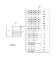
- FIG. 7 shows the means by which the tester 104 will access the chip 103 for testing.
- the tester has ten separate test heads 701 , each capable of testing a chip 103 in parallel with other test heads 701 .
- Each test head 701 can access the chip 103 through a series of pins.
- a plurality of column address bits 702 - 710 may be used to address the column of the stack to be tested.
- a plurality of row address bits 711 - 715 may be used to address the row of the stack to be tested.
- a high voltage pin 716 may be used to provide power to the chip, as well as a voltage to the anode of diodes corresponding to stacks not under test.
- a low voltage pin 717 may be used to provide ground to the chip 103 , as well as a voltage to the cathode of diodes corresponding to stacks not under test.
- a voltage source pin 718 may be used to provide a positive voltage on the cathode side of a diode and stack combination under test.
- a voltage sink pin 719 may be used to provide a voltage relatively smaller than the voltage source on the anode side of a diode and stack combination under test.
- a chip enable pin 720 may be used to enable or disable measurement of current. Current may be measured by the test head 701 by examining the flow of current into the voltage source pin 718 .
- FIG. 8 shows an enhanced embodiment comprising arranging the diode into a P+ substrate, forming a bipolar junction transistor, which allows more current to flow through stack.
- the resolution of the stack resistance calculation increases with the amount of current that can flow through the stack.
- the diode and stack are connected in series, and consequently the diode acts as the limiting factor in the amount of current that can flow through the stack.
- a PNP transistor 801 is formed.
- the current able to flow through the stack 802 be increased by utilizing this transistor.
- second P+ regions 406 are added to access the transistor through its collector terminal 805 .
- the second P+ regions are connected to other P+ regions on other diode and stack combinations.
- the second P+ regions are connected to ground.
- the first P+ region 401 forming the diode connects the stack 802 to the emitter terminal 803 of the transistor.
- the N-Well 402 connects the anode of the diode to the transistor base terminal 804 .
- FIG. 9 demonstrates the circuit equivalent of these elements.
- the via stack 901 is connected in series with the co-doped and salicided polysilicon interconnect 410 and the combination of the diode 902 and the parasitic transistor 903 , the diode 902 and the parasitic transistor 903 being connected in parallel.
- the flow of a small amount of current from the diode 902 into the base of the transistor 903 activates the forward mode of the transistor 903 , causing current to flow through the transistor.
- the result is that more current can flow through the stack 901 .
- structure 410 acts as a low resistance wire interconnect. Only when the silicide layer 410 is improperly formed, for example comprises gaps or is broken, the structure 410 acts as a reversed biased diode preventing any current to flow.
Landscapes
- Engineering & Computer Science (AREA)
- Manufacturing & Machinery (AREA)
- Microelectronics & Electronic Packaging (AREA)
- Power Engineering (AREA)
- Computer Hardware Design (AREA)
- Automation & Control Theory (AREA)
- Semiconductor Integrated Circuits (AREA)
- Testing Or Measuring Of Semiconductors Or The Like (AREA)
- Physics & Mathematics (AREA)
- Ceramic Engineering (AREA)
- Condensed Matter Physics & Semiconductors (AREA)
- General Physics & Mathematics (AREA)
Priority Applications (6)
| Application Number | Priority Date | Filing Date | Title |
|---|---|---|---|
| US13/831,101 US8878183B2 (en) | 2013-03-14 | 2013-03-14 | Method and apparatus for monitoring semiconductor fabrication |
| PCT/US2014/020347 WO2014143586A1 (en) | 2013-03-14 | 2014-03-04 | Method and apparatus for monitoring semiconductor fabrication |
| EP14711413.6A EP2973673A1 (en) | 2013-03-14 | 2014-03-04 | Method and apparatus for monitoring semiconductor fabrication |
| KR1020157029398A KR20150132442A (ko) | 2013-03-14 | 2014-03-04 | 반도체 제조를 모니터링하기 위한 방법 및 장치 |
| CN201480013984.5A CN105144360B (zh) | 2013-03-14 | 2014-03-04 | 用于监视半导体制作的方法及设备 |
| TW103108874A TWI619186B (zh) | 2013-03-14 | 2014-03-13 | 用於監測半導體製造之方法及裝置 |
Applications Claiming Priority (1)
| Application Number | Priority Date | Filing Date | Title |
|---|---|---|---|
| US13/831,101 US8878183B2 (en) | 2013-03-14 | 2013-03-14 | Method and apparatus for monitoring semiconductor fabrication |
Publications (2)
| Publication Number | Publication Date |
|---|---|
| US20140264333A1 US20140264333A1 (en) | 2014-09-18 |
| US8878183B2 true US8878183B2 (en) | 2014-11-04 |
Family
ID=50336571
Family Applications (1)
| Application Number | Title | Priority Date | Filing Date |
|---|---|---|---|
| US13/831,101 Active US8878183B2 (en) | 2013-03-14 | 2013-03-14 | Method and apparatus for monitoring semiconductor fabrication |
Country Status (6)
| Country | Link |
|---|---|
| US (1) | US8878183B2 (zh) |
| EP (1) | EP2973673A1 (zh) |
| KR (1) | KR20150132442A (zh) |
| CN (1) | CN105144360B (zh) |
| TW (1) | TWI619186B (zh) |
| WO (1) | WO2014143586A1 (zh) |
Cited By (1)
| Publication number | Priority date | Publication date | Assignee | Title |
|---|---|---|---|---|
| WO2017152001A1 (en) | 2016-03-03 | 2017-09-08 | Microchip Technology Incorporated | Interconnect monitor utilizing both open and short detection |
Families Citing this family (1)
| Publication number | Priority date | Publication date | Assignee | Title |
|---|---|---|---|---|
| CN112103203B (zh) * | 2020-11-10 | 2021-02-23 | 晶芯成(北京)科技有限公司 | 半导体测试结构及其形成方法、半导体器件的测试方法 |
Citations (4)
| Publication number | Priority date | Publication date | Assignee | Title |
|---|---|---|---|---|
| US6933591B1 (en) | 2003-10-16 | 2005-08-23 | Altera Corporation | Electrically-programmable integrated circuit fuses and sensing circuits |
| KR100774789B1 (ko) | 2006-11-21 | 2007-11-07 | 동부일렉트로닉스 주식회사 | Cmos의 실리사이드 공정 모니터링용 패턴 구조 및 그설계방법 |
| US20080308883A1 (en) | 2007-06-14 | 2008-12-18 | Ji-Ho Hong | Monitoring pattern for silicide |
| US7919973B2 (en) * | 2007-06-22 | 2011-04-05 | Microchip Technology Incorporated | Method and apparatus for monitoring via's in a semiconductor fab |
Family Cites Families (3)
| Publication number | Priority date | Publication date | Assignee | Title |
|---|---|---|---|---|
| US8680653B2 (en) * | 2007-11-12 | 2014-03-25 | Infineon Technologies Ag | Wafer and a method of dicing a wafer |
| CN101370377A (zh) * | 2008-07-11 | 2009-02-18 | 赵永先 | 利用可调节视频线进行芯片定位的方法 |
| US8534302B2 (en) * | 2008-12-09 | 2013-09-17 | Microchip Technology Incorporated | Prober cleaning block assembly |
-
2013
- 2013-03-14 US US13/831,101 patent/US8878183B2/en active Active
-
2014
- 2014-03-04 CN CN201480013984.5A patent/CN105144360B/zh active Active
- 2014-03-04 KR KR1020157029398A patent/KR20150132442A/ko not_active Application Discontinuation
- 2014-03-04 EP EP14711413.6A patent/EP2973673A1/en not_active Ceased
- 2014-03-04 WO PCT/US2014/020347 patent/WO2014143586A1/en active Application Filing
- 2014-03-13 TW TW103108874A patent/TWI619186B/zh active
Patent Citations (4)
| Publication number | Priority date | Publication date | Assignee | Title |
|---|---|---|---|---|
| US6933591B1 (en) | 2003-10-16 | 2005-08-23 | Altera Corporation | Electrically-programmable integrated circuit fuses and sensing circuits |
| KR100774789B1 (ko) | 2006-11-21 | 2007-11-07 | 동부일렉트로닉스 주식회사 | Cmos의 실리사이드 공정 모니터링용 패턴 구조 및 그설계방법 |
| US20080308883A1 (en) | 2007-06-14 | 2008-12-18 | Ji-Ho Hong | Monitoring pattern for silicide |
| US7919973B2 (en) * | 2007-06-22 | 2011-04-05 | Microchip Technology Incorporated | Method and apparatus for monitoring via's in a semiconductor fab |
Non-Patent Citations (1)
| Title |
|---|
| International Search Report and Written Opinion, Application No. PCT/US2014/020347, 13 pages. |
Cited By (2)
| Publication number | Priority date | Publication date | Assignee | Title |
|---|---|---|---|---|
| WO2017152001A1 (en) | 2016-03-03 | 2017-09-08 | Microchip Technology Incorporated | Interconnect monitor utilizing both open and short detection |
| US10177053B2 (en) | 2016-03-03 | 2019-01-08 | Microchip Technology Incorporated | Interconnect monitor utilizing both open and short detection |
Also Published As
| Publication number | Publication date |
|---|---|
| KR20150132442A (ko) | 2015-11-25 |
| CN105144360B (zh) | 2018-07-27 |
| TWI619186B (zh) | 2018-03-21 |
| WO2014143586A1 (en) | 2014-09-18 |
| CN105144360A (zh) | 2015-12-09 |
| US20140264333A1 (en) | 2014-09-18 |
| TW201448080A (zh) | 2014-12-16 |
| EP2973673A1 (en) | 2016-01-20 |
Similar Documents
| Publication | Publication Date | Title |
|---|---|---|
| KR101431708B1 (ko) | 반도체 제조에 있어서의 비아 모니터링 장치 및 방법 | |
| US8664968B2 (en) | On-die parametric test modules for in-line monitoring of context dependent effects | |
| JP5142145B2 (ja) | 半導体装置の製造方法、半導体ウェハ、およびテスト方法 | |
| US9966318B1 (en) | System for electrical testing of through silicon vias (TSVs) | |
| US7807480B2 (en) | Test cells for semiconductor yield improvement | |
| US9767248B2 (en) | Semiconductor having cross coupled structure and layout verification method thereof | |
| US10522430B2 (en) | Semiconductor device | |
| US11996338B2 (en) | Test structure and test method thereof | |
| Wang et al. | Pre-bond testing of the silicon interposer in 2.5 D ICs | |
| US8878183B2 (en) | Method and apparatus for monitoring semiconductor fabrication | |
| US10177053B2 (en) | Interconnect monitor utilizing both open and short detection | |
| Hess et al. | Passive multiplexer test structure for fast and accurate contact and via fail-rate evaluation | |
| Brozek | Short flow characterization vehicle (test chip) usage in advanced technology development and yield improvement | |
| Agam et al. | Yield improvement in dense EEPROM by bit mapping and experimental design | |
| Beaudoin et al. | Yield and Failure Analysis of 14nm On-Chip MIMCAP | |
| Siong et al. | Method to increase defect localization success rate on open failure by combining circuit layout analysis with photon emission microscopy | |
| CN115116872A (zh) | 测试三维集成电路中硅穿孔的电路结构 | |
| Lin et al. | Problems with IO to all other IOs ESD stress test: Two case studies | |
| JP2014138150A (ja) | 半導体装置の検査方法 |
Legal Events
| Date | Code | Title | Description |
|---|---|---|---|
| AS | Assignment |
Owner name: MICROCHIP TECHNOLOGY INCORPORATED, ARIZONA Free format text: ASSIGNMENT OF ASSIGNORS INTEREST;ASSIGNOR:YACH, RANDY;REEL/FRAME:032443/0583 Effective date: 20130313 |
|
| STCF | Information on status: patent grant |
Free format text: PATENTED CASE |
|
| AS | Assignment |
Owner name: JPMORGAN CHASE BANK, N.A., AS ADMINISTRATIVE AGENT, ILLINOIS Free format text: SECURITY INTEREST;ASSIGNOR:MICROCHIP TECHNOLOGY INCORPORATED;REEL/FRAME:041675/0617 Effective date: 20170208 Owner name: JPMORGAN CHASE BANK, N.A., AS ADMINISTRATIVE AGENT Free format text: SECURITY INTEREST;ASSIGNOR:MICROCHIP TECHNOLOGY INCORPORATED;REEL/FRAME:041675/0617 Effective date: 20170208 |
|
| MAFP | Maintenance fee payment |
Free format text: PAYMENT OF MAINTENANCE FEE, 4TH YEAR, LARGE ENTITY (ORIGINAL EVENT CODE: M1551) Year of fee payment: 4 |
|
| AS | Assignment |
Owner name: JPMORGAN CHASE BANK, N.A., AS ADMINISTRATIVE AGENT, ILLINOIS Free format text: SECURITY INTEREST;ASSIGNORS:MICROCHIP TECHNOLOGY INCORPORATED;SILICON STORAGE TECHNOLOGY, INC.;ATMEL CORPORATION;AND OTHERS;REEL/FRAME:046426/0001 Effective date: 20180529 Owner name: JPMORGAN CHASE BANK, N.A., AS ADMINISTRATIVE AGENT Free format text: SECURITY INTEREST;ASSIGNORS:MICROCHIP TECHNOLOGY INCORPORATED;SILICON STORAGE TECHNOLOGY, INC.;ATMEL CORPORATION;AND OTHERS;REEL/FRAME:046426/0001 Effective date: 20180529 |
|
| AS | Assignment |
Owner name: WELLS FARGO BANK, NATIONAL ASSOCIATION, AS NOTES COLLATERAL AGENT, CALIFORNIA Free format text: SECURITY INTEREST;ASSIGNORS:MICROCHIP TECHNOLOGY INCORPORATED;SILICON STORAGE TECHNOLOGY, INC.;ATMEL CORPORATION;AND OTHERS;REEL/FRAME:047103/0206 Effective date: 20180914 Owner name: WELLS FARGO BANK, NATIONAL ASSOCIATION, AS NOTES C Free format text: SECURITY INTEREST;ASSIGNORS:MICROCHIP TECHNOLOGY INCORPORATED;SILICON STORAGE TECHNOLOGY, INC.;ATMEL CORPORATION;AND OTHERS;REEL/FRAME:047103/0206 Effective date: 20180914 |
|
| AS | Assignment |
Owner name: JPMORGAN CHASE BANK, N.A., AS ADMINISTRATIVE AGENT, DELAWARE Free format text: SECURITY INTEREST;ASSIGNORS:MICROCHIP TECHNOLOGY INC.;SILICON STORAGE TECHNOLOGY, INC.;ATMEL CORPORATION;AND OTHERS;REEL/FRAME:053311/0305 Effective date: 20200327 |
|
| AS | Assignment |
Owner name: ATMEL CORPORATION, ARIZONA Free format text: RELEASE BY SECURED PARTY;ASSIGNOR:JPMORGAN CHASE BANK, N.A, AS ADMINISTRATIVE AGENT;REEL/FRAME:053466/0011 Effective date: 20200529 Owner name: MICROCHIP TECHNOLOGY INC., ARIZONA Free format text: RELEASE BY SECURED PARTY;ASSIGNOR:JPMORGAN CHASE BANK, N.A, AS ADMINISTRATIVE AGENT;REEL/FRAME:053466/0011 Effective date: 20200529 Owner name: MICROSEMI STORAGE SOLUTIONS, INC., ARIZONA Free format text: RELEASE BY SECURED PARTY;ASSIGNOR:JPMORGAN CHASE BANK, N.A, AS ADMINISTRATIVE AGENT;REEL/FRAME:053466/0011 Effective date: 20200529 Owner name: SILICON STORAGE TECHNOLOGY, INC., ARIZONA Free format text: RELEASE BY SECURED PARTY;ASSIGNOR:JPMORGAN CHASE BANK, N.A, AS ADMINISTRATIVE AGENT;REEL/FRAME:053466/0011 Effective date: 20200529 Owner name: MICROSEMI CORPORATION, CALIFORNIA Free format text: RELEASE BY SECURED PARTY;ASSIGNOR:JPMORGAN CHASE BANK, N.A, AS ADMINISTRATIVE AGENT;REEL/FRAME:053466/0011 Effective date: 20200529 |
|
| AS | Assignment |
Owner name: WELLS FARGO BANK, NATIONAL ASSOCIATION, MINNESOTA Free format text: SECURITY INTEREST;ASSIGNORS:MICROCHIP TECHNOLOGY INC.;SILICON STORAGE TECHNOLOGY, INC.;ATMEL CORPORATION;AND OTHERS;REEL/FRAME:053468/0705 Effective date: 20200529 |
|
| AS | Assignment |
Owner name: WELLS FARGO BANK, NATIONAL ASSOCIATION, AS COLLATERAL AGENT, MINNESOTA Free format text: SECURITY INTEREST;ASSIGNORS:MICROCHIP TECHNOLOGY INCORPORATED;SILICON STORAGE TECHNOLOGY, INC.;ATMEL CORPORATION;AND OTHERS;REEL/FRAME:055671/0612 Effective date: 20201217 |
|
| AS | Assignment |
Owner name: WELLS FARGO BANK, NATIONAL ASSOCIATION, AS NOTES COLLATERAL AGENT, MINNESOTA Free format text: SECURITY INTEREST;ASSIGNORS:MICROCHIP TECHNOLOGY INCORPORATED;SILICON STORAGE TECHNOLOGY, INC.;ATMEL CORPORATION;AND OTHERS;REEL/FRAME:057935/0474 Effective date: 20210528 |
|
| AS | Assignment |
Owner name: MICROSEMI STORAGE SOLUTIONS, INC., ARIZONA Free format text: RELEASE BY SECURED PARTY;ASSIGNOR:JPMORGAN CHASE BANK, N.A., AS ADMINISTRATIVE AGENT;REEL/FRAME:059333/0222 Effective date: 20220218 Owner name: MICROSEMI CORPORATION, ARIZONA Free format text: RELEASE BY SECURED PARTY;ASSIGNOR:JPMORGAN CHASE BANK, N.A., AS ADMINISTRATIVE AGENT;REEL/FRAME:059333/0222 Effective date: 20220218 Owner name: ATMEL CORPORATION, ARIZONA Free format text: RELEASE BY SECURED PARTY;ASSIGNOR:JPMORGAN CHASE BANK, N.A., AS ADMINISTRATIVE AGENT;REEL/FRAME:059333/0222 Effective date: 20220218 Owner name: SILICON STORAGE TECHNOLOGY, INC., ARIZONA Free format text: RELEASE BY SECURED PARTY;ASSIGNOR:JPMORGAN CHASE BANK, N.A., AS ADMINISTRATIVE AGENT;REEL/FRAME:059333/0222 Effective date: 20220218 Owner name: MICROCHIP TECHNOLOGY INCORPORATED, ARIZONA Free format text: RELEASE BY SECURED PARTY;ASSIGNOR:JPMORGAN CHASE BANK, N.A., AS ADMINISTRATIVE AGENT;REEL/FRAME:059333/0222 Effective date: 20220218 |
|
| AS | Assignment |
Owner name: MICROCHIP TECHNOLOGY INCORPORATED, ARIZONA Free format text: RELEASE BY SECURED PARTY;ASSIGNOR:JPMORGAN CHASE BANK, N.A., AS ADMINISTRATIVE AGENT;REEL/FRAME:059666/0545 Effective date: 20220218 |
|
| AS | Assignment |
Owner name: MICROSEMI STORAGE SOLUTIONS, INC., ARIZONA Free format text: RELEASE BY SECURED PARTY;ASSIGNOR:WELLS FARGO BANK, NATIONAL ASSOCIATION, AS NOTES COLLATERAL AGENT;REEL/FRAME:059358/0001 Effective date: 20220228 Owner name: MICROSEMI CORPORATION, ARIZONA Free format text: RELEASE BY SECURED PARTY;ASSIGNOR:WELLS FARGO BANK, NATIONAL ASSOCIATION, AS NOTES COLLATERAL AGENT;REEL/FRAME:059358/0001 Effective date: 20220228 Owner name: ATMEL CORPORATION, ARIZONA Free format text: RELEASE BY SECURED PARTY;ASSIGNOR:WELLS FARGO BANK, NATIONAL ASSOCIATION, AS NOTES COLLATERAL AGENT;REEL/FRAME:059358/0001 Effective date: 20220228 Owner name: SILICON STORAGE TECHNOLOGY, INC., ARIZONA Free format text: RELEASE BY SECURED PARTY;ASSIGNOR:WELLS FARGO BANK, NATIONAL ASSOCIATION, AS NOTES COLLATERAL AGENT;REEL/FRAME:059358/0001 Effective date: 20220228 Owner name: MICROCHIP TECHNOLOGY INCORPORATED, ARIZONA Free format text: RELEASE BY SECURED PARTY;ASSIGNOR:WELLS FARGO BANK, NATIONAL ASSOCIATION, AS NOTES COLLATERAL AGENT;REEL/FRAME:059358/0001 Effective date: 20220228 |
|
| AS | Assignment |
Owner name: MICROSEMI STORAGE SOLUTIONS, INC., ARIZONA Free format text: RELEASE BY SECURED PARTY;ASSIGNOR:WELLS FARGO BANK, NATIONAL ASSOCIATION, AS NOTES COLLATERAL AGENT;REEL/FRAME:059863/0400 Effective date: 20220228 Owner name: MICROSEMI CORPORATION, ARIZONA Free format text: RELEASE BY SECURED PARTY;ASSIGNOR:WELLS FARGO BANK, NATIONAL ASSOCIATION, AS NOTES COLLATERAL AGENT;REEL/FRAME:059863/0400 Effective date: 20220228 Owner name: ATMEL CORPORATION, ARIZONA Free format text: RELEASE BY SECURED PARTY;ASSIGNOR:WELLS FARGO BANK, NATIONAL ASSOCIATION, AS NOTES COLLATERAL AGENT;REEL/FRAME:059863/0400 Effective date: 20220228 Owner name: SILICON STORAGE TECHNOLOGY, INC., ARIZONA Free format text: RELEASE BY SECURED PARTY;ASSIGNOR:WELLS FARGO BANK, NATIONAL ASSOCIATION, AS NOTES COLLATERAL AGENT;REEL/FRAME:059863/0400 Effective date: 20220228 Owner name: MICROCHIP TECHNOLOGY INCORPORATED, ARIZONA Free format text: RELEASE BY SECURED PARTY;ASSIGNOR:WELLS FARGO BANK, NATIONAL ASSOCIATION, AS NOTES COLLATERAL AGENT;REEL/FRAME:059863/0400 Effective date: 20220228 |
|
| AS | Assignment |
Owner name: MICROSEMI STORAGE SOLUTIONS, INC., ARIZONA Free format text: RELEASE BY SECURED PARTY;ASSIGNOR:WELLS FARGO BANK, NATIONAL ASSOCIATION, AS NOTES COLLATERAL AGENT;REEL/FRAME:059363/0001 Effective date: 20220228 Owner name: MICROSEMI CORPORATION, ARIZONA Free format text: RELEASE BY SECURED PARTY;ASSIGNOR:WELLS FARGO BANK, NATIONAL ASSOCIATION, AS NOTES COLLATERAL AGENT;REEL/FRAME:059363/0001 Effective date: 20220228 Owner name: ATMEL CORPORATION, ARIZONA Free format text: RELEASE BY SECURED PARTY;ASSIGNOR:WELLS FARGO BANK, NATIONAL ASSOCIATION, AS NOTES COLLATERAL AGENT;REEL/FRAME:059363/0001 Effective date: 20220228 Owner name: SILICON STORAGE TECHNOLOGY, INC., ARIZONA Free format text: RELEASE BY SECURED PARTY;ASSIGNOR:WELLS FARGO BANK, NATIONAL ASSOCIATION, AS NOTES COLLATERAL AGENT;REEL/FRAME:059363/0001 Effective date: 20220228 Owner name: MICROCHIP TECHNOLOGY INCORPORATED, ARIZONA Free format text: RELEASE BY SECURED PARTY;ASSIGNOR:WELLS FARGO BANK, NATIONAL ASSOCIATION, AS NOTES COLLATERAL AGENT;REEL/FRAME:059363/0001 Effective date: 20220228 |
|
| AS | Assignment |
Owner name: MICROSEMI STORAGE SOLUTIONS, INC., ARIZONA Free format text: RELEASE BY SECURED PARTY;ASSIGNOR:WELLS FARGO BANK, NATIONAL ASSOCIATION, AS NOTES COLLATERAL AGENT;REEL/FRAME:060894/0437 Effective date: 20220228 Owner name: MICROSEMI CORPORATION, ARIZONA Free format text: RELEASE BY SECURED PARTY;ASSIGNOR:WELLS FARGO BANK, NATIONAL ASSOCIATION, AS NOTES COLLATERAL AGENT;REEL/FRAME:060894/0437 Effective date: 20220228 Owner name: ATMEL CORPORATION, ARIZONA Free format text: RELEASE BY SECURED PARTY;ASSIGNOR:WELLS FARGO BANK, NATIONAL ASSOCIATION, AS NOTES COLLATERAL AGENT;REEL/FRAME:060894/0437 Effective date: 20220228 Owner name: SILICON STORAGE TECHNOLOGY, INC., ARIZONA Free format text: RELEASE BY SECURED PARTY;ASSIGNOR:WELLS FARGO BANK, NATIONAL ASSOCIATION, AS NOTES COLLATERAL AGENT;REEL/FRAME:060894/0437 Effective date: 20220228 Owner name: MICROCHIP TECHNOLOGY INCORPORATED, ARIZONA Free format text: RELEASE BY SECURED PARTY;ASSIGNOR:WELLS FARGO BANK, NATIONAL ASSOCIATION, AS NOTES COLLATERAL AGENT;REEL/FRAME:060894/0437 Effective date: 20220228 |
|
| MAFP | Maintenance fee payment |
Free format text: PAYMENT OF MAINTENANCE FEE, 8TH YEAR, LARGE ENTITY (ORIGINAL EVENT CODE: M1552); ENTITY STATUS OF PATENT OWNER: LARGE ENTITY Year of fee payment: 8 |