US8877520B2 - Ferroelectric film containing a perovskite structure oxide and method for manufacturing a ferroelectric film - Google Patents
Ferroelectric film containing a perovskite structure oxide and method for manufacturing a ferroelectric film Download PDFInfo
- Publication number
- US8877520B2 US8877520B2 US13/749,770 US201313749770A US8877520B2 US 8877520 B2 US8877520 B2 US 8877520B2 US 201313749770 A US201313749770 A US 201313749770A US 8877520 B2 US8877520 B2 US 8877520B2
- Authority
- US
- United States
- Prior art keywords
- film
- ferroelectric film
- ferroelectric
- oriented
- oxygen atmosphere
- Prior art date
- Legal status (The legal status is an assumption and is not a legal conclusion. Google has not performed a legal analysis and makes no representation as to the accuracy of the status listed.)
- Active
Links
Images


Classifications
-
- H—ELECTRICITY
- H10—SEMICONDUCTOR DEVICES; ELECTRIC SOLID-STATE DEVICES NOT OTHERWISE PROVIDED FOR
- H10N—ELECTRIC SOLID-STATE DEVICES NOT OTHERWISE PROVIDED FOR
- H10N30/00—Piezoelectric or electrostrictive devices
- H10N30/01—Manufacture or treatment
- H10N30/09—Forming piezoelectric or electrostrictive materials
- H10N30/093—Forming inorganic materials
-
- H01L41/39—
-
- H01L41/1873—
-
- H01L41/1876—
-
- H01L41/318—
-
- H01L41/319—
-
- H—ELECTRICITY
- H10—SEMICONDUCTOR DEVICES; ELECTRIC SOLID-STATE DEVICES NOT OTHERWISE PROVIDED FOR
- H10N—ELECTRIC SOLID-STATE DEVICES NOT OTHERWISE PROVIDED FOR
- H10N30/00—Piezoelectric or electrostrictive devices
- H10N30/01—Manufacture or treatment
- H10N30/07—Forming of piezoelectric or electrostrictive parts or bodies on an electrical element or another base
- H10N30/074—Forming of piezoelectric or electrostrictive parts or bodies on an electrical element or another base by depositing piezoelectric or electrostrictive layers, e.g. aerosol or screen printing
- H10N30/077—Forming of piezoelectric or electrostrictive parts or bodies on an electrical element or another base by depositing piezoelectric or electrostrictive layers, e.g. aerosol or screen printing by liquid phase deposition
- H10N30/078—Forming of piezoelectric or electrostrictive parts or bodies on an electrical element or another base by depositing piezoelectric or electrostrictive layers, e.g. aerosol or screen printing by liquid phase deposition by sol-gel deposition
-
- H—ELECTRICITY
- H10—SEMICONDUCTOR DEVICES; ELECTRIC SOLID-STATE DEVICES NOT OTHERWISE PROVIDED FOR
- H10N—ELECTRIC SOLID-STATE DEVICES NOT OTHERWISE PROVIDED FOR
- H10N30/00—Piezoelectric or electrostrictive devices
- H10N30/01—Manufacture or treatment
- H10N30/07—Forming of piezoelectric or electrostrictive parts or bodies on an electrical element or another base
- H10N30/074—Forming of piezoelectric or electrostrictive parts or bodies on an electrical element or another base by depositing piezoelectric or electrostrictive layers, e.g. aerosol or screen printing
- H10N30/079—Forming of piezoelectric or electrostrictive parts or bodies on an electrical element or another base by depositing piezoelectric or electrostrictive layers, e.g. aerosol or screen printing using intermediate layers, e.g. for growth control
-
- H—ELECTRICITY
- H10—SEMICONDUCTOR DEVICES; ELECTRIC SOLID-STATE DEVICES NOT OTHERWISE PROVIDED FOR
- H10N—ELECTRIC SOLID-STATE DEVICES NOT OTHERWISE PROVIDED FOR
- H10N30/00—Piezoelectric or electrostrictive devices
- H10N30/80—Constructional details
- H10N30/85—Piezoelectric or electrostrictive active materials
- H10N30/853—Ceramic compositions
- H10N30/8542—Alkali metal based oxides, e.g. lithium, sodium or potassium niobates
-
- H—ELECTRICITY
- H10—SEMICONDUCTOR DEVICES; ELECTRIC SOLID-STATE DEVICES NOT OTHERWISE PROVIDED FOR
- H10N—ELECTRIC SOLID-STATE DEVICES NOT OTHERWISE PROVIDED FOR
- H10N30/00—Piezoelectric or electrostrictive devices
- H10N30/80—Constructional details
- H10N30/85—Piezoelectric or electrostrictive active materials
- H10N30/853—Ceramic compositions
- H10N30/8548—Lead-based oxides
- H10N30/8554—Lead-zirconium titanate [PZT] based
Definitions
- the present invention relates to a technology of changing and controlling arbitrarily the orientation of a ferroelectric film to be crystallized.
- PZT Pb(Zr,Ti)O 3
- a SiO 2 film having a thickness of 300 nm is formed, and, on the SiO 2 film, a TiO x film having a thickness of 5 nm is formed.
- a Pt film having a thickness of 150 nm oriented, for example, in (111) is formed, and, on the Pt film, a PZT sol-gel solution is spin-coated with a spin coater.
- the spin condition at this time is such that the wafer is rotated for 30 seconds at a rotation rate of 1500 rpm and for 10 seconds at a rotation rate of 4000 rpm.
- the coated PZT sol-gel solution is heated and held on a hot plate at 250° C. for 30 seconds to be dried and the moisture was eliminated, and, after that, in addition, the solution is heated and held for 60 seconds on a hot plate kept at high temperature of 500° C., and thus temporary calcinations is performed.
- a PZT amorphous thin film having a thickness of 150 nm is produced.
- annealing treatment was performed on the PZT amorphous thin film by using a pressurizing-type lamp annealing apparatus (RTA: rapidly thermal anneal), to crystallize the PZT.
- RTA pressurizing-type lamp annealing apparatus
- the crystallization annealing at this time was performed under conditions in which the thin film was heated up to 700° C. at a temperature increase rate of 100° C./sec and held for 1 min, at respective oxygen partial pressures of 1 atm, 5 atm and 10 atm.
- the PZT film thus crystallized is composed of a perovskite structure (see, for example, Patent Document 1 (WO 2006/087777)).
- PZT films crystallized at each of oxygen partial pressures of the above-described 1 atm, 5 atm and 10 atm were evaluated by X-ray diffraction (hereinafter, represented as “XRD”) measurement.
- XRD X-ray diffraction
- FIG. 8 is a drawing showing an XRD pattern of the PZT film crystallized at an oxygen partial pressure of the above-described 10 atm, in which the vertical axis shows an XRD reflection intensity and the horizontal axis shows a rotation angle 2 ⁇ . From FIG. 8 , it is known that the PZT film is crystallized, but in the industrial world, a ferroelectric material film having further higher crystallinity is required.
- An aspect of the present invention aims at further accelerating the crystallization of a ferroelectric film. Furthermore, an aspect of the present invention aims at further improving the crystallinity of a ferroelectric film. Moreover, an aspect of the present invention aims at arbitrarily controlling the orientation of a ferroelectric film to be crystallized.
- a method for manufacturing a ferroelectric film including the steps of:
- a method for manufacturing a ferroelectric film including the steps of:
- an amorphous thin film including a burnable material containing hydrogen of not less than 1% by weight (preferably not less than 10% by weight) and a ferroelectric material;
- the first ferroelectric film includes at least one of:
- A is at least one kind selected from the group consisting of Li, Na, K, Rb, Pb, Ca, Sr, Ba, Bi, La and Hf
- B is at least one kind selected from the group consisting of Ru, Fe, Ti, Zr, Nb, Ta, V, W and Mo
- m is a natural number of not more than 5
- Trm 2 Ba 2 Ca n ⁇ 1 Cu n O 2n+4 or TrmBa 2 Ca n ⁇ 1 Cu n O 2n+3 (where, Lan is at least one kind selected from the group consisting of Y, La, Ce, Pr, Nd, Pm, Sm, Eu, Gd, Tb, Dy, Ho, Er, Tm, Yb and Lu, Trm is at least one kind selected from the group consisting of Bi, Tl and Hg, and n is a natural number of not more than 5);
- tungsten bronze structure oxide represented by A 0.5 BO 3 (tetragonal bronze structure) or A 0.3 BO 3 (hexagonal bronze structure) (where, A is at least one kind selected from the group consisting of Li, Na, K, Rb, Cs, Pb, Ca, Sr, Ba, Bi and La, and B is at least one kind selected from the group consisting of Ru, Fe, Ti, Zr, Nb, Ta, V, W and Mo);
- the first ferroelectric film includes a perovskite structure oxide
- the first ferroelectric film is oriented in any of (001), (001)+(110), (110), (110)+(111), and (111), when the amorphous thin film is heated in an oxygen atmosphere, by increase in an oxygen supply amount, as a pressurized oxygen atmosphere.
- a pressure of the pressurized oxygen atmosphere when the first ferroelectric film is oriented in (001) is lower than a pressure of the pressurized oxygen atmosphere when the first ferroelectric film is oriented in (001)+(110);
- a pressure of the pressurized oxygen atmosphere when the first ferroelectric film is oriented in (001)+(110) is lower than a pressure of the pressurized oxygen atmosphere when the first ferroelectric film is oriented in (110);
- a pressure of the pressurized oxygen atmosphere when the first ferroelectric film is oriented in (110) is lower than a pressure of the pressurized oxygen atmosphere when the first ferroelectric film is oriented in (110)+(111);
- a pressure of the pressurized oxygen atmosphere when the first ferroelectric film is oriented in (110)+(111) is lower than a pressure of the pressurized oxygen atmosphere when the first ferroelectric film is oriented in (111).
- the first ferroelectric film includes a perovskite structure oxide
- the first ferroelectric film is oriented in any of (001), (001)+(110), (110), (110)+(111) and (111) by increasing a thickness of the burnable material film.
- a thickness of the burnable material film when the first ferroelectric film is oriented in (001) is smaller than a thickness of the burnable material film when the first ferroelectric film is oriented in (001)+(110);
- a thickness of the burnable material film when the first ferroelectric film is oriented in (001)+(110) is smaller than a thickness of the burnable material film when the first ferroelectric film is oriented in (110);
- a thickness of the burnable material film when the first ferroelectric film is oriented in (110) is smaller than a thickness of the burnable material film when the first ferroelectric film is oriented in (110)+(111);
- a thickness of the burnable material film when the first ferroelectric film is oriented in (110)+(111) is smaller than a thickness of the burnable material film when the first ferroelectric film is oriented in (111).
- the burnable material film is a DLC film having a thickness of 0.1 nm to 300 nm.
- the first ferroelectric film is a PZT film.
- an electrode is formed on the substrate.
- the first ferroelectric film is formed on the electrode.
- a thickness of the amorphous thin film is 5 nm to 450 nm.
- a ferroelectric film comprising a perovskite structure oxide, wherein
- a half-value width of the strongest peak in measurement results of any of (001), (110) and (111) orientations by X-ray diffraction is not more than 1.5° (preferably not more than 0.75°, more preferably not more than 0.4°).
- the crystallization of a ferroelectric material film can be further accelerated. Furthermore, by applying an aspect of the present invention, the crystallinity of a ferroelectric material film can be further improved. Moreover, by applying an aspect of the present invention, the orientation of a ferroelectric film to be crystallized can be arbitrarily controlled.
- FIG. 1 is a cross-sectional view for describing the method for manufacturing the PZT film according to Example 1 of the present invention.
- FIG. 2 is a drawing showing XRD patterns of each of samples 1 and 2 in Example 1 measured with a parallel beam optical system.
- FIG. 3 is a drawing showing XRD patterns of each of samples 3 and 4 in Example 1 measured with a parallel beam optical system.
- FIG. 4 is a drawing showing an XRD pattern obtained by measuring a sample 1 in Example 2.
- FIG. 5 is a drawing showing an XRD pattern obtained by measuring a sample 2 in Example 2.
- FIG. 6 is a drawing showing an XRD pattern obtained by measuring a sample 3 in Example 2.
- FIG. 7 is a drawing showing an XRD pattern obtained by measuring a sample 1 in Example 4.
- FIG. 8 is a drawing showing an XRD pattern of a conventional PZT film.
- an electrode On a substrate, an electrode is formed.
- a Pt film oriented in a prescribed crystalline plane, for example, in (111) is used.
- a Pt film is used as the electrode, but various ones may be used as long as they function as an electrode.
- such a material as Au, Ag, Pa or Ir may be used.
- a burnable material film containing hydrogen of not less than 1% by weight (preferably not less than 10% by weight, more preferably to 80% by weight, further preferably 30 to 60% by weight) is formed.
- the burnable material film is a film to be burned and disappearing in a later crystallization process heated in an oxygen atmosphere, and is a film that discharges hydrogen contained in the film in the burning.
- a C x N y H z film, a carbon film or a diamond-like carbon film (hereinafter referred to as “a DLC film”) formed, for example, by a CVD method may be used.
- x, y and z satisfy Formulae (i) and (ii), preferably (i′) to (iv′) below.
- the C x N y H z film for example, any of C 4 H 2 N 2 , C 5 H 3 N 3 , C 7 H 3 N 3 , C 6 H 2 N 4 , C 5 H 2 N 4 , C 10 H 2 N 4 , C 12 H 4 N 4 and C 6 N 4 may be used.
- the C x N y H z film is used as the burnable material film, hydrogen and nitrogen contained in the film is discharged in the burning in the later crystallization process of the heating in an oxygen atmosphere.
- the thickness thereof may be, for example, 0.1 nm to 300 nm.
- a first amorphous thin film including a first ferroelectric material is formed on the burnable material film.
- the thickness of the first amorphous thin film may be 5 to 450 nm (preferably 20 to 150 nm).
- the first ferroelectric material is a material to be a film composed of any of (1) to (6) below by the crystallization of the first amorphous thin film in a later crystallization process.
- Perovskite and bismuth layered structure oxides represented by ABO 3 or (Bi 2 O 2 ) 2+ (A m ⁇ 1 B m O 3m+1 ) 2 ⁇ (where, A is at least one kind selected from the group consisting of Li, Na, K, Rb, Pb, Ca, Sr, Ba, Bi, La and Hf, B is at least one kind selected from the group consisting of Ru, Fe, Ti, Zr, Nb, Ta, V, W and Mo, and m is a natural number of not more than 5).
- Tungsten bronze structure oxides represented by A 0.5 BO 3 (tetragonal bronze structure) or A 0.3 BO 3 (hexagonal bronze structure) (where, A is at least one kind selected from the group consisting of Li, Na, K, Rb, Cs, Pb, Ca, Sr, Ba, Bi and La, and B is at least one kind selected from the group consisting of Ru, Fe, Ti, Zr, Nb, Ta, V, W and Mo).
- a material including SiO 2 in the above-mentioned at least one kind of material is a material including SiO 2 in the above-mentioned at least one kind of material.
- a material including SiO 2 and GeO 2 in the above-mentioned at least one kind of material is a material including SiO 2 and GeO 2 in the above-mentioned at least one kind of material.
- the burnable material film is burned, and at this time, hydrogen is discharged, and, while the hydrogen is supplied to the first amorphous thin film, the first amorphous thin film is oxidized and crystallized. Consequently, on the electrode, the first ferroelectric film is formed.
- the crystallization is caused by oxidation of the first amorphous thin film with oxygen along with the reduction of the film with hydrogen.
- the oxidization along with the reduction with hydrogen means that alkali metals such as Li, Na, K and Rb in the first amorphous thin film are reduced to be kept as pure alkali metals and the pure alkali metals are oxidized with oxygen.
- the utilization of reduction action with hydrogen makes it possible to further accelerate the oxidation of the alkali metal for crystallization.
- the crystallization of the first amorphous thin film can be further accelerated, and the crystallinity of the first ferroelectric film can be further improved.
- the first ferroelectric film is composed of a perovskite structure oxide
- a pressurized oxygen atmosphere may be utilized to increase the oxygen supply amount. Consequently, the first ferroelectric film is oriented in any of (001), (001)+(110), (110), (110)+(111) and (111).
- the pressure of a pressurized oxygen atmosphere when the first ferroelectric film is oriented in (001) is lower than that of a pressurized oxygen atmosphere when the first ferroelectric film is oriented in (001)+(110). Furthermore, the pressure of a pressurized oxygen atmosphere when the first ferroelectric film is oriented in (001)+(110) is lower than that of a pressurized oxygen atmosphere when the first ferroelectric film is oriented in (110). Moreover, the pressure of a pressurized oxygen atmosphere when the first ferroelectric film is oriented in (110) is lower than that of a pressurized oxygen atmosphere when the first ferroelectric film is oriented in (110)+(111).
- the pressure of a pressurized oxygen atmosphere when the first ferroelectric film is oriented in (110)+(111) is lower than that of a pressurized oxygen atmosphere when the first ferroelectric film is oriented in (111).
- the orientation of the crystalline plane of the first ferroelectric film can be controlled.
- the first ferroelectric film is composed of a perovskite structure oxide
- the first ferroelectric film is oriented in any of (001), (001)+(110), (110), (110)+(111), and (111).
- the thickness of a burnable material film when the first ferroelectric film is oriented in (001) is smaller than that of a burnable material film when the first ferroelectric film is oriented in (001)+(110). Furthermore, the thickness of a burnable material film when the first ferroelectric film is oriented in (001)+(110) is smaller than that of a burnable material film when the first ferroelectric film is oriented in (110). Moreover, the thickness of a burnable material film when the first ferroelectric film is oriented in (110) is smaller than that of a burnable material film when the first ferroelectric film is oriented in (110)+(111).
- the thickness of a burnable material film when the first ferroelectric film is oriented in (110)+(111) is smaller than that of a burnable material film when the first ferroelectric film is oriented in (111).
- the orientation of the crystalline plane of the first ferroelectric film can be controlled.
- the PZT film is oriented, for example, in any of (001), (001)+(110), and (110).
- the burnable material film is, for example, a DLC film having a thickness of 10 ⁇ m and the first ferroelectric film is, for example, a PZT film having a thickness of 2 to 4 ⁇ m
- the PZT film is oriented in (001).
- the burnable material film is, for example, a DLC film having a thickness of 20 ⁇ m and the first ferroelectric film is, for example, a PZT film having a thickness of 2 to 4 ⁇ m
- the PZT film is oriented in (001)+(110), in which (001) is stronger in orientation intensity.
- the burnable material film is, for example, a DLC film having a thickness of 50 ⁇ m and the first ferroelectric film is, for example, a PZT film having a thickness of 2 to 4 ⁇ m
- the PZT film is oriented in (110)+(001), in which (110) is stronger in orientation intensity.
- the burnable material film is, for example, a DLC film having a thickness of 100 ⁇ m and the first ferroelectric film is, for example, a PZT film having a thickness of 2 to 4 ⁇ m
- the PZT film is oriented in (110)+(001), in which (110) is considerably stronger in orientation intensity.
- the first ferroelectric film produced as described above is used as an initial nucleus to form a second amorphous thin film containing a second ferroelectric material on the first ferroelectric film.
- the thickness of the second amorphous thin film may be thicker than that of the first amorphous thin film.
- the second ferroelectric material the material that is the same as the first ferroelectric material may be used.
- the second amorphous thin film is oxidized and crystallized. Consequently, on the first ferroelectric film, a second ferroelectric film is formed. Since the first ferroelectric film is used as an initial nucleus in the crystallization, the second ferroelectric film has the same orientation of crystalline plane as that of the first ferroelectric film.
- the crystallinity of each of the first and second ferroelectric films produced as described above can be further improved.
- an electronic component may be produced.
- the present embodiment is the same as the first embodiment except for the following point.
- the present embodiment there is used a process of forming, on an electrode, a first amorphous thin film including a burnable material containing hydrogen of not less than 1% by weight (preferably not less than 10% by weight, more preferably to 80% by weight, further more preferably 30 to 60% by weight) and the first ferroelectric material.
- first amorphous thin film After forming the above-described first amorphous thin film, heating was performed on the first amorphous thin film in an oxygen atmosphere to burn the burnable material in the first amorphous thin film and cause the burnable material to disappear. At this time, hydrogen is discharged and, while the hydrogen is supplied to the first amorphous thin film, the first amorphous thin film is oxidized and crystallized. Consequently, on the electrode, the first ferroelectric film is formed.
- the role of the hydrogen in the crystallization is the same as that in the first embodiment, and thus, by utilizing the reduction action of hydrogen, the oxidation for crystallization can be further accelerated. As the result, the crystallization of the first amorphous thin film can be further accelerated, and the crystallinity of the first ferroelectric film can be further improved.
- carbon powder that supports hydrogen can be used as the burnable material.
- a method for supporting hydrogen for example, hydrogen can be supported easily by immersing porous carbon powder in acetone.
- carbon powder covered with a C x N y H z film or a DLC film containing hydrogen there can be used.
- a CVD method or a sputtering method the same C x N y H z film as that in the first embodiment can be used.
- FIG. 1 is a cross-sectional view for describing the method for manufacturing the PZT film according to Example 1 of the present invention.
- the manufacturing method of the PZT film is a manufacturing method of a PZT film on a substrate, which is a manufacturing method of a ferroelectric ceramic thin film by using a carbon film such as a DLC film as the burnable material film.
- substrates for producing samples 1 to 4 were prepared.
- the substrate there was used one having a 200 nm-thick SiO 2 film 2 formed on a 6-inch Si substrate 1, having a 30 nm-thick TiO x film 3 formed on the SiO 2 film 2 and a (111)-oriented 200 nm-thick Pt electrode thin film 4 formed on the TiO x film 3.
- a 10 nm-thick DLC film which is a carbon film 5 as a burnable material film
- a 20 nm-thick DLC film which is the carbon film 5 as the burnable material film
- a 50 nm-thick DLC film which is the carbon film 5 as the burnable material film
- a 100 nm-thick DLC film which is the carbon film 5 as the burnable material film
- a 10 nm-thick DLC film was formed on the Pt electrode thin film 4 of the substrate of the sample 1, by placing the substrate of the sample 1 on a substrate electrode in a chamber of a parallel plate type plasma CVD apparatus (not shown), introducing toluene into the chamber at a flow rate of 30 sccm as a raw material gas, setting the pressure in the chamber to be 0.5 Pa, keeping the substrate temperature at room temperature (substrate was not heated), supplying radio frequency waves of 13.56 MHz to the substrate electrode at an output of 900 W, and forming a film in prescribed film-forming time.
- a 10 nm-thick DLC film was formed on the Pt electrode thin film 4 of the substrate of the sample 2, by placing the substrate of the sample 2 on a substrate electrode in a chamber of a parallel plate type plasma CVD apparatus (not shown), introducing toluene into the chamber at a flow rate of 30 sccm as a raw material gas, setting the pressure in the chamber to be 0.5 Pa, keeping the substrate temperature at room temperature (substrate was not heated), supplying radio frequency waves of 13.56 MHz to the substrate electrode at an output of 900 W, and forming a film in prescribed film-forming time.
- a 10 nm-thick DLC film was formed on the Pt electrode thin film 4 of the substrate of the sample 3, by placing the substrate of the sample 3 on a substrate electrode in a chamber of a parallel plate type plasma CVD apparatus (not shown), introducing toluene into the chamber at a flow rate of 30 sccm as a raw material gas, setting the pressure in the chamber to be 0.5 Pa, keeping the substrate temperature at room temperature (substrate was not heated), supplying radio frequency waves of 13.56 MHz to the substrate electrode at an output of 900 W, and forming a film in prescribed film-forming time.
- a 100 nm-thick DLC film was formed on the Pt electrode thin film 4 of the substrate of the sample 4, by placing the substrate of the sample 4 on a substrate electrode in a chamber of a parallel plate type plasma CVD apparatus (not shown), introducing toluene into the chamber at a flow rate of 30 sccm as a raw material gas, setting the pressure in the chamber to be 0.5 Pa, keeping the substrate temperature at room temperature (substrate was not heated), supplying radio frequency waves of 13.56 MHz to the substrate electrode at an output of 900 W, and forming a film in prescribed film-forming time.
- the flow rate of toluene in film forming is set to be 30 sccm, but the flow rate of a raw material gas in film forming may be set to be in a range of 3 to 100 sccm.
- the pressure in the chamber in film forming is set to be 0.5 Pa, but the pressure in the chamber in film forming may be set to be in a range of 0.1 to 20 Pa.
- the substrate temperature in film forming is set to be room temperature, but the substrate temperature in film forming may be set to be in a range of room temperature to 300° C.
- the electric power of output 900 W is supplied to the substrate electrode in film forming, but an electric power in a power density range of 0.01 to 5.00 W/cm 2 may be supplied to the substrate electrode in film forming.
- a PZT film 6 was formed by a spin coating method. Methods for forming these PZT films 6 are as follows.
- a sol-gel solution for forming a PZT ferroelectric thin film an E1 solution of 10% by weight concentration in which 20% of lead was added excessively in a solvent of butanol (manufactured by Mitsubishi Materials Corporation) was used.
- the E1 solution was spin-coated with a spin coater.
- the spin coater for example, MS-A200 (manufactured by MIKASA CO., LTD) was used.
- the coater was rotated at 800 rpm for 5 sec and at 1500 rpm for 10 sec, and, then, the rotation rate was gradually increased to 3000 rpm in 10 sec. After that, it was left on a hot plate (ceramic hot plate AHS-300, manufactured by AS ONE Corporation) at 150° C. for 5 min in the air, left on the hot plate (AHS-300) at 300° C. for min in the air, and then cooled to room temperature.
- a PZT amorphous thin film having an intended thickness was formed.
- a thermal oxidation treatment was performed on PZT amorphous thin films of substrates of samples 1 to 4 by using a rapid heating furnace (RTA), to thereby crystallize PZT amorphous thin films.
- RTA rapid heating furnace
- the conditions of the thermal treatment at this time were such that temperature was raised to 700° C. at an increase rate of 100° C./sec, held for 5 min and then cooled, in an O 2 100% atmosphere and a pressurized circumstance of 9.9 atm.
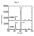
- the PZT film of the sample 1 (No. 12) exhibited a strong (001) orientation
- the PZT film of the sample 2 (No. 13) exhibited a strong (001) orientation and a weak (110) orientation.
- the PZT film of the sample 3 (50M0) exhibited a strong (110) orientation and a weak (001) orientation
- the PZT film of the sample 4 (100M0) exhibited a very strong (110) orientation and a weak (001) orientation.
- the carbon film 5 such as a DLC film as the burnable material film
- all the DLC film burns and changes into CO 2 at the same time as the crystallization, that is, oxidation of the PZT film 6. Therefore, large benefits can be obtained in which carbon does not diffuse into the PZT film 6, and in which, as the result, properties of the PZT film 6 are not deteriorated.
- the hydrogen amount contained in the DLC film is preferably not less than 1% by weight, more preferably not less than 10% by weight, much more preferably 10 to 80% by weight, and furthermore preferably 30 to 60% by weight.
- the carbon film 5 such as the DLC film as a buffer layer may remain or disappear after crystallizing the PZT amorphous thin film, depending on the thickness, film forming conditions and the like thereof.
- the orientation of the PZT film 6 can be controlled arbitrarily.
- the (001)-oriented PZT film obtained in the present Example can be applied to electronic components such as an actuator and MEMS, the (111)-oriented PZT film can be applied to an electronic component such as FRAM (registered trademark), and the (110)-oriented PZT film can be applied to an electronic component such as a SAW device.
- electronic components such as an actuator and MEMS
- the (111)-oriented PZT film can be applied to an electronic component such as FRAM (registered trademark)
- the (110)-oriented PZT film can be applied to an electronic component such as a SAW device.
- Three substrates for producing samples 1 to 3 were prepared.
- the substrate there was used one having a 300 nm-thick SiO 2 film formed on a 6-inch Si (100) substrate, having formed a 5 nm-thick TiO x film formed on the SiO 2 film and having a (111)-oriented 150 nm-thick Pt electrode thin film formed on the TiO, film.
- a PZT film was formed by a spin coating method.
- the method for forming these PZT films is as follows.
- the solution was spin-coated with a spin coater.
- the spin coater for example, MS-A200 (manufactured by MIKASA CO., LTD) was used. The spin conditions are such that the substrate is rotated at 1500 rpm for 30 sec, and then, rotated at 4000 rpm for 10 sec.
- the coated film was left on a hot plate (ceramic hot plate AHS-300, manufactured by AS ONE Corporation) at 250° C. for 30 sec in the air, and was subjected to temporary calcination at 500° C. for 60 sec. Therefore, a PZT amorphous thin film having an intended thickness was formed.
- a hot plate ceramic hot plate AHS-300, manufactured by AS ONE Corporation
- a thermal oxidation treatment was performed on PZT amorphous thin films of substrates of samples 1 to 3 by using a rapid heating furnace (RTA), to thereby crystallize PZT amorphous thin films.
- the conditions of the thermal treatment at this time were such that, for the sample 1, temperature was raised to 700° C. at an increase rate of 100° C./sec, held for 1 min and then cooled, in an O 2 100% atmosphere and an ordinary pressure circumstance of 1 atm, for the sample 2, temperature was raised to 700° C. at an increase rate of 100° C./sec, held for 1 min and then cooled, in an O 2 100% atmosphere and a pressurized circumstance of 5 atm and, for the sample 3, temperature was raised to 700° C.
- the PZT film thus formed had a composition of Pb(Zr 0.3 Ti 0.7 )O 3 .
- FIG. 4 An XRD pattern by measuring the sample 1 thus obtained is shown in FIG. 4
- FIG. 5 An XRD pattern by measuring the sample 2 is shown in FIG. 5
- FIG. 6 An XRD pattern by measuring the sample 3 is shown in FIG. 6 .
- the vertical axis shows an XRD reflection intensity and the horizontal axis shows a rotation angle 2 ⁇ .
- the PZT film of the sample 1 exhibited a strong (001) orientation
- the PZT film of the sample 2 exhibited a strong (110) orientation
- the PZT film of the sample 3 exhibited a strong (111) orientation.
- the orientation of the PZT film can be controlled to be (001), (110) and (111).
- a thick PZT film was formed by a spin coating method.
- a method for forming these thick PZT films is as follows.
- the solution was spin-coated with a spin coater.
- the spin coater for example, MS-A200 (manufactured by MIKASA CO., LTD) was used. The spin conditions are such that the substrate is rotated at 1500 rpm for 30 sec, and then, rotated at 4000 rpm for 10 sec.
- the coated film was left on a hot plate (ceramic hot plate AHS-300, manufactured by AS ONE Corporation) at 250° C. for 30 sec in the air, and was subjected to temporary calcination at 500° C. for 60 sec. Then, the above-mentioned spin coating, drying and temporary calcination were performed continuously 25 times. Consequently, a thick PZT amorphous film was formed.
- a hot plate ceramic hot plate AHS-300, manufactured by AS ONE Corporation
- a thermal oxidation treatment was performed on PZT amorphous thick films of the substrates of the samples 1 to 3 by using a rapid heating furnace (RTA), to thereby crystallize PZT amorphous thick films.
- the conditions of the thermal treatment at this time were such that, for the sample 1, temperature was raised to 700° C. at an increase rate of 100° C./sec, held for 1 min and then cooled, in an O 2 100% atmosphere and an ordinary pressure circumstance of 1 atm, for the sample 2, temperature was raised to 700° C. at an increase rate of 100° C./sec, held for 1 min and then cooled, in an O 2 100% atmosphere and a pressurized circumstance of 5 atm and, for the sample 3, temperature was raised to 700° C. at an increase rate of 100° C./sec, held for 1 min and then cooled, in an O 2 100% atmosphere and a pressurized circumstance of 10 atm.
- samples 1 to 3 were subjected to a post-annealing treatment.
- the conditions at this time were such that temperature was raised to 800° C. at an increase rate of 100° C./sec, held for 10 min and then cooled, in an O 2 100% atmosphere and a pressurized circumstance of 10 atm.
- the PZT thick film thus produced had a thickness of 4.5 ⁇ m and a composition of Pb (Zr 0.52 Ti 0.48 )O 3 .
- the PZT thick film of the sample 1 exhibited a strong (001) orientation
- the PZT thick film of the sample 2 exhibited a strong (110) orientation
- the PZT thick film of the sample 3 exhibited a strong (111) orientation.
- the orientation of the PZT film can be controlled to be (001), (110) and (111).
- the PZT thick film has the same orientation of the crystalline plane as the PZT film.
- a substrate for producing sample 1 was prepared.
- the substrate there was used one having a 300 nm-thick SiO 2 film formed on a 6-inch Si (100) substrate, having formed a 5 nm-thick TiO x film formed on the SiO 2 film, and having a (111)-oriented 150 nm-thick Pt electrode thin film formed on the TiO x film.
- a 10 nm DLC film as the burnable material film was formed on the Pt electrode thin film of the substrate of the sample 1.
- the DLC film contains hydrogen.
- the method for forming the DLC film is the same as the method in Example 1.
- a KNN film composed of a perovskite structure that is, (K 1-X Na X )NbO 3 film (0.3 ⁇ X ⁇ 0.7) was formed by a spin coating method.
- the method for forming the KNN film is as follows.
- the solution was spin-coated with a spin coater.
- the spin coater for example, MS-A200 (manufactured by MIKASA CO., LTD) was used. The spin conditions are such that the solution is rotated at 1500 rpm for 30 sec, and then, rotated at 4000 rpm for sec.
- the coated film was left on a hot plate (ceramic hot plate AHS-300, manufactured by AS ONE Corporation) at 250° C. for 30 sec in the air, and was subjected to temporary calcination at 500° C. for 60 sec. Therefore, a KNN amorphous thin film having an intended thickness was formed.
- a hot plate ceramic hot plate AHS-300, manufactured by AS ONE Corporation
- a thermal oxidation treatment was performed on the KNN amorphous thin film of the substrate of the sample 1 by using a rapid heating furnace (RTA), to thereby crystallize the KNN amorphous thin film.
- RTA rapid heating furnace
- the conditions of the thermal treatment at this time were such that temperature was raised to 700° C. at an increase rate of 100° C./sec, held for 1 min and then cooled, in an O 2 100% atmosphere and an ordinary pressure circumstance of 1 atm.
- the KNN film thus produced had a composition of (K 0.5 Na 0.5 )NbO 3 .
- FIG. 7 An XRD pattern by measuring the sample 1 thus obtained is shown in FIG. 7 .
- the vertical axis shows an XRD reflection intensity and the horizontal axis shows a rotation angle 2 ⁇ .
- the KNN film of the sample 1 exhibited a strong (001) orientation.
- Ferroelectric films according to Examples 1 to 4 are composed of a perovskite structure oxide, and the half-value width of the strongest peak in measurement results of any of (001), (110) and (111) orientations by X-ray diffraction was not more than 0.30. Note that the half-value width may be not more than 1.50 (more preferably not more than 0.75°, further more preferably not more than 0.4°).
Landscapes
- Engineering & Computer Science (AREA)
- Chemical & Material Sciences (AREA)
- Manufacturing & Machinery (AREA)
- Ceramic Engineering (AREA)
- Materials Engineering (AREA)
- Dispersion Chemistry (AREA)
- Inorganic Chemistry (AREA)
- Formation Of Insulating Films (AREA)
- Semiconductor Memories (AREA)
Abstract
Description
0.1≦z (i)
x+y+z=1 (ii)
0.1≦z (i)
x+y+z=1 (ii)
0<x (i′)
0<y (ii′)
0.1≦z (iii′)
x+y+z=1 (iv′)
Claims (21)
0.1≦z (i)
x+y+z=1 (ii).
Applications Claiming Priority (2)
| Application Number | Priority Date | Filing Date | Title |
|---|---|---|---|
| JP2012-15597 | 2012-01-27 | ||
| JP2012015597A JP5891490B2 (en) | 2012-01-27 | 2012-01-27 | Method for manufacturing ferroelectric film |
Publications (2)
| Publication Number | Publication Date |
|---|---|
| US20130192878A1 US20130192878A1 (en) | 2013-08-01 |
| US8877520B2 true US8877520B2 (en) | 2014-11-04 |
Family
ID=48869291
Family Applications (1)
| Application Number | Title | Priority Date | Filing Date |
|---|---|---|---|
| US13/749,770 Active US8877520B2 (en) | 2012-01-27 | 2013-01-25 | Ferroelectric film containing a perovskite structure oxide and method for manufacturing a ferroelectric film |
Country Status (2)
| Country | Link |
|---|---|
| US (1) | US8877520B2 (en) |
| JP (1) | JP5891490B2 (en) |
Cited By (1)
| Publication number | Priority date | Publication date | Assignee | Title |
|---|---|---|---|---|
| US12266710B2 (en) | 2021-06-04 | 2025-04-01 | Samsung Electronics Co., Ltd. | Thin film structure, semiconductor device including the same, and semiconductor apparatus including semiconductor device |
Families Citing this family (5)
| Publication number | Priority date | Publication date | Assignee | Title |
|---|---|---|---|---|
| CN103938133B (en) * | 2014-03-27 | 2016-02-24 | 中原工学院 | A kind of take Zirconium oxide fibre as polycrystalline diamond of toughness reinforcing phase and preparation method thereof |
| JP6596634B2 (en) * | 2014-10-23 | 2019-10-30 | アドバンストマテリアルテクノロジーズ株式会社 | Ferroelectric ceramics, electronic parts, and manufacturing method of ferroelectric ceramics |
| CN106478096A (en) * | 2015-08-31 | 2017-03-08 | 中国民航大学 | A kind of rare earth base novel non-full of type tungsten bronze ferroelectric material and preparation method thereof |
| US11121139B2 (en) * | 2017-11-16 | 2021-09-14 | International Business Machines Corporation | Hafnium oxide and zirconium oxide based ferroelectric devices with textured iridium bottom electrodes |
| WO2020029069A1 (en) | 2018-08-07 | 2020-02-13 | 济南晶正电子科技有限公司 | Micron-scale single-crystal thin film |
Citations (6)
| Publication number | Priority date | Publication date | Assignee | Title |
|---|---|---|---|---|
| US20050019493A1 (en) * | 2001-02-02 | 2005-01-27 | Micron Technology, Inc. | Method for controlling deposition of dielectric films |
| WO2006087777A1 (en) | 2005-02-16 | 2006-08-24 | Youtec Co., Ltd. | Pressurizing type lamp annealing device, pressurizing type lamp annealing method, thin-film, and electronic component |
| US20090230821A1 (en) * | 2001-06-13 | 2009-09-17 | Seiko Epson Corporation | Ceramic and method of manufacturing the same, dielectric capacitor, semiconductor device, and element |
| JP2011029399A (en) * | 2009-07-24 | 2011-02-10 | Utec:Kk | Ferroelectric film, electronic component, and method of manufacturing the ferroelectric film |
| US20110275163A1 (en) * | 2006-08-03 | 2011-11-10 | Ahn Kie Y | Zr-SUBSTITUTED BaTiO3 FILMS |
| US20120295099A1 (en) * | 2011-05-17 | 2012-11-22 | Mitsubishi Materials Corporation | Method for producing ferroelectric thin film |
Family Cites Families (10)
| Publication number | Priority date | Publication date | Assignee | Title |
|---|---|---|---|---|
| JPH04259380A (en) * | 1991-02-13 | 1992-09-14 | Mitsubishi Materials Corp | Method for controlling crystalline orientation property of pzt ferroelectric body thin film |
| US5866238A (en) * | 1994-05-05 | 1999-02-02 | Minolta Co., Ltd. | Ferroelectric thin film device and its process |
| JP3517876B2 (en) * | 1998-10-14 | 2004-04-12 | セイコーエプソン株式会社 | Ferroelectric thin film element manufacturing method, ink jet recording head, and ink jet printer |
| JP4437178B2 (en) * | 2000-02-04 | 2010-03-24 | 国立大学法人東京工業大学 | Deposition method of ferroelectric material thin film and its application |
| JP2003046065A (en) * | 2001-07-30 | 2003-02-14 | Sony Corp | Ferroelectric nonvolatile semiconductor memory and method of manufacturing the same |
| JP4300765B2 (en) * | 2002-07-29 | 2009-07-22 | 株式会社村田製作所 | Oriented ferroelectric thin film device |
| JP4221576B2 (en) * | 2003-03-10 | 2009-02-12 | セイコーエプソン株式会社 | Ceramic film manufacturing method, ferroelectric capacitor manufacturing method, ceramic film, ferroelectric capacitor, and semiconductor device |
| JP2006210896A (en) * | 2004-12-27 | 2006-08-10 | Fuji Photo Film Co Ltd | Film deposition method, structure and piezoelectric element manufactured using the same, and liquid discharge head manufacturing method |
| JP5568913B2 (en) * | 2009-07-24 | 2014-08-13 | 株式会社ユーテック | PZT film manufacturing method and steam heating apparatus |
| JP2011103420A (en) * | 2009-11-12 | 2011-05-26 | Seiko Epson Corp | Piezoelectric element, piezoelectric actuator, liquid jet head, and liquid jet apparatus |
-
2012
- 2012-01-27 JP JP2012015597A patent/JP5891490B2/en not_active Expired - Fee Related
-
2013
- 2013-01-25 US US13/749,770 patent/US8877520B2/en active Active
Patent Citations (9)
| Publication number | Priority date | Publication date | Assignee | Title |
|---|---|---|---|---|
| US20050019493A1 (en) * | 2001-02-02 | 2005-01-27 | Micron Technology, Inc. | Method for controlling deposition of dielectric films |
| US20090230821A1 (en) * | 2001-06-13 | 2009-09-17 | Seiko Epson Corporation | Ceramic and method of manufacturing the same, dielectric capacitor, semiconductor device, and element |
| US20100207492A1 (en) * | 2001-06-13 | 2010-08-19 | Seiko Epson Corporation | Ceramic and method of manufacturing the same, Dielectric capacitor, semiconductor device, and element |
| US20100289384A1 (en) * | 2001-06-13 | 2010-11-18 | Seiko Epson Corporation | Ceramic and method of manufacturing the same, dielectric capacitor, semiconductor device, and element |
| US7960901B2 (en) * | 2001-06-13 | 2011-06-14 | Seiko Epson Corporation | Piezoelectric device having a ferroelectric film including a ferroelectric material |
| WO2006087777A1 (en) | 2005-02-16 | 2006-08-24 | Youtec Co., Ltd. | Pressurizing type lamp annealing device, pressurizing type lamp annealing method, thin-film, and electronic component |
| US20110275163A1 (en) * | 2006-08-03 | 2011-11-10 | Ahn Kie Y | Zr-SUBSTITUTED BaTiO3 FILMS |
| JP2011029399A (en) * | 2009-07-24 | 2011-02-10 | Utec:Kk | Ferroelectric film, electronic component, and method of manufacturing the ferroelectric film |
| US20120295099A1 (en) * | 2011-05-17 | 2012-11-22 | Mitsubishi Materials Corporation | Method for producing ferroelectric thin film |
Cited By (1)
| Publication number | Priority date | Publication date | Assignee | Title |
|---|---|---|---|---|
| US12266710B2 (en) | 2021-06-04 | 2025-04-01 | Samsung Electronics Co., Ltd. | Thin film structure, semiconductor device including the same, and semiconductor apparatus including semiconductor device |
Also Published As
| Publication number | Publication date |
|---|---|
| JP5891490B2 (en) | 2016-03-23 |
| JP2013157401A (en) | 2013-08-15 |
| US20130192878A1 (en) | 2013-08-01 |
Similar Documents
| Publication | Publication Date | Title |
|---|---|---|
| JP5509419B2 (en) | Ferroelectric film, electronic component, and method for manufacturing ferroelectric film | |
| US8877520B2 (en) | Ferroelectric film containing a perovskite structure oxide and method for manufacturing a ferroelectric film | |
| JP5740645B2 (en) | Oriented perovskite oxide thin films | |
| JP4424332B2 (en) | Method for manufacturing piezoelectric thin film element | |
| US20170170384A1 (en) | Crystal film, method for manufacturing crystal film, vapor deposition apparatus and multi-chamber apparatus | |
| Jung et al. | Enhancement of energy storage and thermal stability of relaxor Pb0. 92La0. 08Zr0. 52Ti0. 48O3-Bi (Zn0. 66Nb0. 33) O3 thick films through aerosol deposition | |
| US10243134B2 (en) | Piezoelectric film and piezoelectric ceramics | |
| US20130165313A1 (en) | Ferroelectric film, sol-gel solution, film forming method and method for manufacturing ferroelectric film | |
| JP5370346B2 (en) | Piezoelectric element and ink jet recording head | |
| US10115887B2 (en) | Ferroelectric ceramics and method for manufacturing the same | |
| WO2010047177A1 (en) | Method for producing metal oxide thin film | |
| JP2015201624A (en) | piezoelectric composition and piezoelectric element | |
| JP6149222B2 (en) | Ferroelectric film manufacturing apparatus and ferroelectric film manufacturing method | |
| JP2008198396A (en) | Method for producing superconducting oxide material | |
| US8030247B2 (en) | Synthesizing precursor solution enabling fabricating biaxially textured buffer layers by low temperature annealing | |
| CN101388434B (en) | Preparation method of silicon/lanthanum strontium cobaltate/lead zirconate titanate three-layer structure ferroelectric material | |
| CN110937925A (en) | A kind of bismuth ferrite-based thin film with high polarization strength and large strain characteristics and preparation method thereof | |
| KR20070110237A (en) | Field Variable Type PS-PJ Pyroclaw Composite Dielectric Thin Film and Manufacturing Method | |
| JP6813758B2 (en) | Ferroelectric ceramics and their manufacturing methods | |
| JPH0695443B2 (en) | Method of manufacturing ferroelectric thin film | |
| Lee et al. | Phase development of radio-frequency magnetron sputter-deposited Pb (Mg 1/3 Nb 2/3) O 3–PbTiO 3 (90/10) thin films | |
| Wang et al. | Preparation and properties of SrBi2. 2 Ta2O9 thin film | |
| KR100591931B1 (en) | Field-variable P-type pyroclaw dielectric thin film and manufacturing method | |
| He et al. | New preparation process of Pb (ZrxTi1− x) O3 thin films from PbZrO3 and PbTiO3 multilayers | |
| Du et al. | Structure evolution and stoichiometry control of Pb (Zr, Ti) O3 thick films fabricated by electrospray assisted vapour deposition |
Legal Events
| Date | Code | Title | Description |
|---|---|---|---|
| AS | Assignment |
Owner name: YOUTEC CO., LTD., JAPAN Free format text: ASSIGNMENT OF ASSIGNORS INTEREST;ASSIGNORS:KIJIMA, TAKESHI;HONDA, YUUJI;HAYAKAWA, HARUHITO;AND OTHERS;SIGNING DATES FROM 20130215 TO 20130225;REEL/FRAME:029921/0754 |
|
| STCF | Information on status: patent grant |
Free format text: PATENTED CASE |
|
| MAFP | Maintenance fee payment |
Free format text: PAYMENT OF MAINTENANCE FEE, 4TH YR, SMALL ENTITY (ORIGINAL EVENT CODE: M2551) Year of fee payment: 4 |
|
| AS | Assignment |
Owner name: ADVANCED MATERIAL TECHNOLOGIES, INC., JAPAN Free format text: CHANGE OF NAME;ASSIGNOR:YOUTEC CO., LTD.;REEL/FRAME:046463/0924 Effective date: 20180509 |
|
| AS | Assignment |
Owner name: UMI I INVESTMENT LIMITED PARTNERSHIP, JAPAN Free format text: SECURITY INTEREST;ASSIGNOR:ADVANCED MATERIAL TECHNOLOGIES, INC.;REEL/FRAME:058763/0517 Effective date: 20210701 |
|
| MAFP | Maintenance fee payment |
Free format text: PAYMENT OF MAINTENANCE FEE, 8TH YR, SMALL ENTITY (ORIGINAL EVENT CODE: M2552); ENTITY STATUS OF PATENT OWNER: SMALL ENTITY Year of fee payment: 8 |
|
| AS | Assignment |
Owner name: KRYSTAL INC., JAPAN Free format text: ASSIGNMENT OF ASSIGNORS INTEREST;ASSIGNOR:ADVANCED MATERIAL TECHNOLOGIES, INC.;REEL/FRAME:060572/0227 Effective date: 20220527 Owner name: UMI I INVESTMENT LIMITED PARTNERSHIP, JAPAN Free format text: RELEASE BY SECURED PARTY;ASSIGNOR:ADVANCED MATERIAL TECHNOLOGIES, INC.;REEL/FRAME:060572/0037 Effective date: 20220624 Owner name: KRYSTAL INC., JAPAN Free format text: ASSIGNMENT OF ASSIGNOR'S INTEREST;ASSIGNOR:ADVANCED MATERIAL TECHNOLOGIES, INC.;REEL/FRAME:060572/0227 Effective date: 20220527 Owner name: UMI I INVESTMENT LIMITED PARTNERSHIP, JAPAN Free format text: RELEASE OF SECURITY INTEREST;ASSIGNOR:ADVANCED MATERIAL TECHNOLOGIES, INC.;REEL/FRAME:060572/0037 Effective date: 20220624 |