US8858709B1 - Silicon carbide with low nitrogen content and method for preparation - Google Patents
Silicon carbide with low nitrogen content and method for preparation Download PDFInfo
- Publication number
- US8858709B1 US8858709B1 US11/784,971 US78497107A US8858709B1 US 8858709 B1 US8858709 B1 US 8858709B1 US 78497107 A US78497107 A US 78497107A US 8858709 B1 US8858709 B1 US 8858709B1
- Authority
- US
- United States
- Prior art keywords
- crucible
- growth
- growth crucible
- gas
- source material
- Prior art date
- Legal status (The legal status is an assumption and is not a legal conclusion. Google has not performed a legal analysis and makes no representation as to the accuracy of the status listed.)
- Active, expires
Links
- 238000000034 method Methods 0.000 title claims abstract description 40
- IJGRMHOSHXDMSA-UHFFFAOYSA-N Atomic nitrogen Chemical compound N#N IJGRMHOSHXDMSA-UHFFFAOYSA-N 0.000 title claims description 92
- 229910052757 nitrogen Inorganic materials 0.000 title claims description 46
- HBMJWWWQQXIZIP-UHFFFAOYSA-N silicon carbide Chemical compound [Si+]#[C-] HBMJWWWQQXIZIP-UHFFFAOYSA-N 0.000 title description 40
- 229910010271 silicon carbide Inorganic materials 0.000 title description 39
- 239000013078 crystal Substances 0.000 claims abstract description 61
- 238000010926 purge Methods 0.000 claims abstract description 61
- 239000000463 material Substances 0.000 claims abstract description 29
- 239000002244 precipitate Substances 0.000 claims abstract description 8
- 238000010438 heat treatment Methods 0.000 claims abstract description 6
- 238000005240 physical vapour deposition Methods 0.000 claims abstract description 5
- 239000007789 gas Substances 0.000 claims description 95
- OKTJSMMVPCPJKN-UHFFFAOYSA-N Carbon Chemical compound [C] OKTJSMMVPCPJKN-UHFFFAOYSA-N 0.000 claims description 30
- 229910002804 graphite Inorganic materials 0.000 claims description 28
- 239000010439 graphite Substances 0.000 claims description 28
- 239000011261 inert gas Substances 0.000 claims description 13
- XKRFYHLGVUSROY-UHFFFAOYSA-N Argon Chemical compound [Ar] XKRFYHLGVUSROY-UHFFFAOYSA-N 0.000 claims description 10
- 230000035699 permeability Effects 0.000 claims description 10
- 229910052734 helium Inorganic materials 0.000 claims description 7
- 239000001307 helium Substances 0.000 claims description 7
- SWQJXJOGLNCZEY-UHFFFAOYSA-N helium atom Chemical compound [He] SWQJXJOGLNCZEY-UHFFFAOYSA-N 0.000 claims description 7
- 229910052786 argon Inorganic materials 0.000 claims description 5
- 239000001257 hydrogen Substances 0.000 claims description 4
- 229910052739 hydrogen Inorganic materials 0.000 claims description 4
- 229910052710 silicon Inorganic materials 0.000 claims description 4
- XUIMIQQOPSSXEZ-UHFFFAOYSA-N Silicon Chemical compound [Si] XUIMIQQOPSSXEZ-UHFFFAOYSA-N 0.000 claims description 3
- 229910052799 carbon Inorganic materials 0.000 claims description 3
- 239000000460 chlorine Substances 0.000 claims description 3
- 238000009413 insulation Methods 0.000 claims description 3
- 239000010703 silicon Substances 0.000 claims description 3
- 125000004435 hydrogen atom Chemical class [H]* 0.000 claims 2
- ZAMOUSCENKQFHK-UHFFFAOYSA-N Chlorine atom Chemical compound [Cl] ZAMOUSCENKQFHK-UHFFFAOYSA-N 0.000 claims 1
- PXGOKWXKJXAPGV-UHFFFAOYSA-N Fluorine Chemical compound FF PXGOKWXKJXAPGV-UHFFFAOYSA-N 0.000 claims 1
- 229910052801 chlorine Inorganic materials 0.000 claims 1
- 239000011737 fluorine Substances 0.000 claims 1
- 229910052731 fluorine Inorganic materials 0.000 claims 1
- 230000008569 process Effects 0.000 description 11
- 239000012535 impurity Substances 0.000 description 6
- 238000000859 sublimation Methods 0.000 description 6
- 230000008022 sublimation Effects 0.000 description 6
- 235000012431 wafers Nutrition 0.000 description 5
- 238000011109 contamination Methods 0.000 description 4
- 230000007547 defect Effects 0.000 description 4
- 238000009792 diffusion process Methods 0.000 description 4
- 238000001914 filtration Methods 0.000 description 4
- 239000000758 substrate Substances 0.000 description 4
- 238000012986 modification Methods 0.000 description 3
- 230000004048 modification Effects 0.000 description 3
- 238000001004 secondary ion mass spectrometry Methods 0.000 description 3
- 239000000126 substance Substances 0.000 description 3
- 229910002704 AlGaN Inorganic materials 0.000 description 2
- 239000000654 additive Substances 0.000 description 2
- 230000004075 alteration Effects 0.000 description 2
- 238000006243 chemical reaction Methods 0.000 description 2
- 238000005229 chemical vapour deposition Methods 0.000 description 2
- 238000007796 conventional method Methods 0.000 description 2
- 238000010586 diagram Methods 0.000 description 2
- 238000010790 dilution Methods 0.000 description 2
- 239000012895 dilution Substances 0.000 description 2
- 230000000694 effects Effects 0.000 description 2
- 230000005012 migration Effects 0.000 description 2
- 238000013508 migration Methods 0.000 description 2
- 239000000203 mixture Substances 0.000 description 2
- 239000011148 porous material Substances 0.000 description 2
- 239000000376 reactant Substances 0.000 description 2
- 239000004065 semiconductor Substances 0.000 description 2
- 241000894007 species Species 0.000 description 2
- 229910052720 vanadium Inorganic materials 0.000 description 2
- LEONUFNNVUYDNQ-UHFFFAOYSA-N vanadium atom Chemical compound [V] LEONUFNNVUYDNQ-UHFFFAOYSA-N 0.000 description 2
- UFHFLCQGNIYNRP-UHFFFAOYSA-N Hydrogen Chemical compound [H][H] UFHFLCQGNIYNRP-UHFFFAOYSA-N 0.000 description 1
- 241000334993 Parma Species 0.000 description 1
- VYPSYNLAJGMNEJ-UHFFFAOYSA-N Silicium dioxide Chemical compound O=[Si]=O VYPSYNLAJGMNEJ-UHFFFAOYSA-N 0.000 description 1
- RTAQQCXQSZGOHL-UHFFFAOYSA-N Titanium Chemical compound [Ti] RTAQQCXQSZGOHL-UHFFFAOYSA-N 0.000 description 1
- 239000000370 acceptor Substances 0.000 description 1
- 238000013459 approach Methods 0.000 description 1
- 239000007795 chemical reaction product Substances 0.000 description 1
- 238000003795 desorption Methods 0.000 description 1
- 239000002019 doping agent Substances 0.000 description 1
- 230000009977 dual effect Effects 0.000 description 1
- -1 first of all Substances 0.000 description 1
- 239000005350 fused silica glass Substances 0.000 description 1
- 150000004820 halides Chemical class 0.000 description 1
- 150000002431 hydrogen Chemical class 0.000 description 1
- 238000004519 manufacturing process Methods 0.000 description 1
- 239000002243 precursor Substances 0.000 description 1
- 239000000047 product Substances 0.000 description 1
- 150000003384 small molecules Chemical class 0.000 description 1
- 238000001179 sorption measurement Methods 0.000 description 1
- 229910052719 titanium Inorganic materials 0.000 description 1
- 239000010936 titanium Substances 0.000 description 1
Images


Classifications
-
- C—CHEMISTRY; METALLURGY
- C30—CRYSTAL GROWTH
- C30B—SINGLE-CRYSTAL GROWTH; UNIDIRECTIONAL SOLIDIFICATION OF EUTECTIC MATERIAL OR UNIDIRECTIONAL DEMIXING OF EUTECTOID MATERIAL; REFINING BY ZONE-MELTING OF MATERIAL; PRODUCTION OF A HOMOGENEOUS POLYCRYSTALLINE MATERIAL WITH DEFINED STRUCTURE; SINGLE CRYSTALS OR HOMOGENEOUS POLYCRYSTALLINE MATERIAL WITH DEFINED STRUCTURE; AFTER-TREATMENT OF SINGLE CRYSTALS OR A HOMOGENEOUS POLYCRYSTALLINE MATERIAL WITH DEFINED STRUCTURE; APPARATUS THEREFOR
- C30B23/00—Single-crystal growth by condensing evaporated or sublimed materials
-
- C—CHEMISTRY; METALLURGY
- C30—CRYSTAL GROWTH
- C30B—SINGLE-CRYSTAL GROWTH; UNIDIRECTIONAL SOLIDIFICATION OF EUTECTIC MATERIAL OR UNIDIRECTIONAL DEMIXING OF EUTECTOID MATERIAL; REFINING BY ZONE-MELTING OF MATERIAL; PRODUCTION OF A HOMOGENEOUS POLYCRYSTALLINE MATERIAL WITH DEFINED STRUCTURE; SINGLE CRYSTALS OR HOMOGENEOUS POLYCRYSTALLINE MATERIAL WITH DEFINED STRUCTURE; AFTER-TREATMENT OF SINGLE CRYSTALS OR A HOMOGENEOUS POLYCRYSTALLINE MATERIAL WITH DEFINED STRUCTURE; APPARATUS THEREFOR
- C30B11/00—Single-crystal growth by normal freezing or freezing under temperature gradient, e.g. Bridgman-Stockbarger method
- C30B11/002—Crucibles or containers for supporting the melt
-
- C—CHEMISTRY; METALLURGY
- C30—CRYSTAL GROWTH
- C30B—SINGLE-CRYSTAL GROWTH; UNIDIRECTIONAL SOLIDIFICATION OF EUTECTIC MATERIAL OR UNIDIRECTIONAL DEMIXING OF EUTECTOID MATERIAL; REFINING BY ZONE-MELTING OF MATERIAL; PRODUCTION OF A HOMOGENEOUS POLYCRYSTALLINE MATERIAL WITH DEFINED STRUCTURE; SINGLE CRYSTALS OR HOMOGENEOUS POLYCRYSTALLINE MATERIAL WITH DEFINED STRUCTURE; AFTER-TREATMENT OF SINGLE CRYSTALS OR A HOMOGENEOUS POLYCRYSTALLINE MATERIAL WITH DEFINED STRUCTURE; APPARATUS THEREFOR
- C30B29/00—Single crystals or homogeneous polycrystalline material with defined structure characterised by the material or by their shape
- C30B29/10—Inorganic compounds or compositions
- C30B29/36—Carbides
Definitions
- the present invention relates to growing crystals, such as silicon carbide (SiC) crystals, with a low content of unintentional nitrogen impurity.
- Wafers of semi-insulating silicon carbide of 4H and 6H polytypes serve as lattice-matched substrates to grow epitaxial layers of SiC and AlGaN, which are used for the fabrication of SiC- and AlGaN-based microwave devices.
- the substrate In order for the device to work efficiently, the substrate must be semi-insulating, that is, fully compensated electronically. In practical terms, this means that the resistivity of the SiC substrate must be higher than 10 5 Ohm ⁇ cm, as measured at room temperature and under normal room light.
- SiC crystals contain impurities and point defects, each with characteristic electronic levels in the bandgap.
- the levels that lay close to the edges of the bandgap are called “shallow”.
- nitrogen is a shallow donor.
- the levels positioned closer to the midgap are called “deep”. Vanadium and certain point defects produce deep levels in silicon carbide.
- the net shallow impurity concentration in a semiconductor is defined as the absolute value of N D -N A , where N D and N A are the concentrations of shallow donors and acceptors, respectively.
- a semiconductor is fully compensated when the concentration of deep levels is higher than the net shallow impurity concentration. Doping with vanadium and introduction of deep point defects has been used for electronic compensation of silicon carbide.
- Unintentional nitrogen donors can be present in SiC crystals at levels as high as 2 ⁇ 10 17 cm ⁇ 3 .
- concentration of deep levels should be higher.
- introduction of deep levels in high concentrations is technologically difficult and can cause stress and generation of defects.
- a better approach to full compensation would be through a reduced presence of unintentional shallow impurities, first of all, nitrogen.
- PVT Physical Vapor Transport
- FIG. 1 A schematic diagram of conventional PVT is shown in FIG. 1 .
- a polycrystalline SiC source 2 is loaded at the bottom of a graphite crucible 1 , and a SiC seed 4 , desirably a single crystal SiC seed 4 , is disposed at the top on the lid.
- the crucible 1 is heated to a growth temperature, generally, between 2000° C. and 2400° C., where source 2 vaporizes and fills the crucible with volatile molecular species of Si 2 C, SiC 2 and Si.
- the source 2 temperature is higher than the seed 4 temperature.
- PVT growth is carried out under a small pressure of inert gas, generally between several and 200 Torr.
- inert gas generally between several and 200 Torr.
- Conventional PVT is a “closed” process in which the Si-bearing vapors do not leave the container, except unintentional losses that can occur through the joint between the crucible body and lid.
- SiC crystals have also been grown using an “open” process.
- a deliberate gas flow is established between the crucible interior and exterior. Examples include High Temperature Chemical Vapor Deposition (HTCVD), Halide Chemical Vapor Deposition (HCVD) and some PVT modifications.
- HTCVD High Temperature Chemical Vapor Deposition
- HCVD Halide Chemical Vapor Deposition
- FIG. 2 A generalized diagram of an open SiC crystal growth process is shown in FIG. 2 .
- a gas mixture 11 that may contain Si and C precursors, dopants and/or other reactants enters crucible 10 through inlet 12 . Inside crucible 10 , the reactants undergo chemical transformations in a reaction zone 14 . The reaction products blend with the vapors originating from the polycrystalline SiC source 13 and move toward a SiC seed 17 , where they precipitate and form crystal 15 . Gaseous products escape through outlet(s) 16 in the lid of crucible 10 .
- Graphite is widely utilized in SiC crystal growth as a material for crucibles and other parts. Due to the chemical nature and porosity of graphite, it is capable of adsorbing large quantities of air, for instance, up to 100 cc of air per gram of graphite. Upon heating to high temperatures, graphite releases the adsorbed gas, thus becoming one of the principal sources of nitrogen contamination in SiC crystal growth. The present inventors have discovered that another source of nitrogen contamination is N 2 from the growth station chamber filtering into the crucible interior through the permeable graphite wall of the crucible.
- Nitrogen contamination in SiC crystal growth can be reduced to some extent using common and well-known conventional techniques.
- One such technique is evacuation and purge of the chamber with pure inert gas. This technique, however, fails to achieve complete removal of nitrogen from graphite bulk.
- Another conventional method is based on the use of getters such as titanium. However, application of getters in the conditions of PVT growth is difficult and can lead to severe contamination of the crystal.
- a better purity with respect to nitrogen can be achieved in open growth processes, such as HTCVD and HCVD, where the nitrogen concentration in the grown crystals can be reduced to below 10 16 cm ⁇ 3 . This can be attributed to the “dilution” effect of the flowing gas and/or to the presence of hydrogen in the growth atmosphere.
- these open growth processes failed to demonstrate high crystal yields, mostly due to the very high losses of silicon-bearing vapors escaping through the crucible outlet(s).
- the present invention is a method for growing SiC crystals, desirably SiC single crystals, with low content of unintentional nitrogen impurity.
- SiC sublimation growth is carried out in a sealed growth crucible made of graphite.
- the thickness of the crucible wall is selected to achieve sufficient permeability of the crucible to inert gases and gaseous nitrogen.
- a flow of purging gas is established in the crystal growth chamber with the purging gas being a pure inert gas containing a very low concentration of residual nitrogen.
- the purging flow can be either external with respect to the growth crucible or internal. In the latter case, the purging gas enters the crucible through an inlet and leaves by filtering through the crucible wall.
- the grown crystals are characterized by the concentration of unintentional nitrogen donor below 2 ⁇ 10 16 cm ⁇ 3 and resistivity above 10 5 ohm ⁇ cm.
- the invention is a physical vapor deposition method of growing a crystal comprising (a) providing a source crucible charged with source material inside of a growth crucible that is at least in-part gas permeable to an unwanted gas that that is present in the charged growth crucible; (b) providing a seed crystal in the growth crucible in spaced relation to the source crucible; (c) heating the interior of the growth crucible whereupon the source material is at a first temperature sufficient to sublimate the source material and the seed crystal is at a second, lower temperature sufficient to cause the sublimated source material to be transported to the seed crystal where the sublimated source material precipitates; and (d) concurrent with step (c), causing a purging gas to flow either inside or outside of the growth crucible, which is also permeable to the purging gas, in a manner whereupon the unwanted gas flows from the inside to the outside of the growth crucible via the gas permeable part thereof.
- An exterior wall of the source crucible can be spaced from an interior wall of the growth crucible.
- the unwanted gas can be nitrogen.
- the purging gas can be an inert gas.
- the growth crucible can be made from graphite.
- the source material and/or the seed crystal can be made from SiC.
- the purging gas can be caused to flow inside the growth crucible at a flow rate between 10 standard cubic centimeters per minute (sccm) and 200 sccm.
- the method can further include providing the growth crucible inside of an insulated chamber with an exterior wall of the growth crucible spaced from an interior wall of the chamber and causing the purging gas to flow through the space between the exterior wall of the growth crucible and the interior wall of the chamber.
- the purging gas can be caused to flow in said space at a flow rate between 100 sccm and 500 sccm.
- the invention is also a physical vapor deposition method of growing a crystal comprising (a) providing a seed crystal and a source material in spaced relation inside of a growth crucible that is at least in-part gas permeable to an unwanted gas therein; (b) heating the growth crucible whereupon the source material sublimates and is transported via a temperature gradient in the growth crucible to the seed crystal where the sublimated source material precipitates; and (c) concurrent with step (b), causing a purging gas to flow inside or outside of the growth crucible in a manner whereupon the unwanted gas flows from the inside to the outside of the growth crucible via the gas permeable part thereof.
- the purging gas can be caused to flow inside the growth crucible at a rate between 10 standard cubic centimeters per minute (sccm) and 200 sccm.
- the source material can be disposed in a source crucible that is positioned inside the growth crucible.
- At least an exterior wall of the source crucible can be spaced from an interior wall of the growth crucible.
- the purging gas can be caused to flow outside the growth crucible at a rate between 100 standard cubic centimeters per minute (sccm) and 500 sccm between an exterior of the growth crucible and an interior of an insulated chamber in which the growth crucible is disposed.
- sccm standard cubic centimeters per minute
- the insulated chamber can include around the growth crucible a porous insulation that facilitates the flow of the purging gas.
- FIGS. 1 and 2 are cross-sectional views of growth vessels for growing crystals, especially silicon carbide crystals, in accordance with the prior art
- FIG. 3 is a cross-sectional view of a system for growing crystals in accordance with one embodiment of the present invention.
- FIG. 4 is a cross-sectional view of a system for growing crystals in accordance with another embodiment of the present invention.
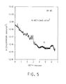
- FIG. 5 is a graph of concentration versus depth of a single wafer extracted from a crystal boule grown utilizing the system shown in FIG. 3 .
- graphite is permeable to inert gases and nitrogen, but has a vastly lower permeability to the vapors formed during sublimation of silicon carbide: Si, Si 2 C and SiC 2 . Accordingly, in the present invention, graphite can be used as a selective filter during SiC sublimation growth—it allows the flow of an inert gas and nitrogen, while restricting the flow of Si-bearing vapors.
- growth crucible 21 is made of graphite, hereinafter, growth crucible 21 .
- growth crucible 21 is made of high-density, fine-grain and low-porosity graphite, such as ATJ isomolded graphite available from GrafTech International, LTD of Parma, Ohio, USA, or similar.
- Growth crucible 21 is loaded with polycrystalline SiC source material 22 and a seed 28 in such a fashion that seed 28 is disposed at the crucible top, while source 22 is disposed in a lower portion of growth crucible 21 .
- Source 22 is desirably contained in a thin-walled graphite crucible called a source crucible 23 .
- the dimensions of the crucibles are such that a gap exists between the outer wall of source crucible 23 and the inner wall of growth crucible 21 . In the preferred embodiment, this gap is between 2 and 10 mm wide; more desirably, it is between 4 and 7 mm wide.
- Chamber 25 includes an insulation that serves the dual propose of retaining heat in growth crucible 21 while enabling a gas (discussed hereinafter) to flow from a gas inlet to a gas outlet of chamber 25 .
- a gas discussed hereinafter
- the illustration of chamber 25 having a gas inlet and a gas outlet at the top and bottom sides thereof is not to be construed as limiting the invention since it is envisioned that the functions of the gas inlet and gas outlet can be reversed if desired.
- chamber 25 Prior to growth, chamber 25 is evacuated and purged with a suitable pure inert gas, such as argon or helium, in accordance with the common practice of the conventional PVT process. Following this step, chamber 25 is filled with pure inert gas to a desired pressure, which is, desirably, between several and 200 Torr, and the temperature within crucible 21 is raised to the growth temperature, which is, desirably, between 2000° C. and 2400° C. Crucible 21 is heated in such a fashion that the temperature of source 22 becomes higher than the temperature of seed 28 , with the temperature difference desirably between 10° C. and 200° C. As a result, Si, Si 2 C and SiC 2 molecules sublimed from source 22 are transported to the seed 28 and precipitate on it, causing growth of crystal 24 .
- a suitable pure inert gas such as argon or helium
- the growing SiC crystal 24 Due to the high chemical affinity for nitrogen, the growing SiC crystal 24 , generally, absorbs nitrogen from the growth crucible atmosphere, thus acting during growth as a nitrogen sink. This lowers the nitrogen partial pressure in growth crucible 21 and, in the conventional PVT process, creates harmful nitrogen flows within the porous wall of growth crucible 21 directed toward the interior thereof. These flows include the flow of nitrogen released from the bulk of the crucible wall and the flow of nitrogen from chamber 25 .
- a flow of high-purity purging gas 26 is supplied continuously during the growth of crystal 24 into chamber 25 .
- This gas purge reduces the supply of nitrogen into the interior of growth crucible 21 and, thus, reduces the level of unintentional nitrogen in crystal 24 .
- a high-purity inert gas 26 desirably argon or helium, is used as a purging gas.
- the purging gas has a low concentration of residual nitrogen, desirably less than 100 ppb of nitrogen and, more desirably less than 10 ppb of nitrogen.
- FIG. 3 One embodiment of the present invention, referred to as an exterior purge, is shown in FIG. 3 .
- purging gas 26 is supplied continuously during growth into chamber 25 . Due to the dilution and direct removal of nitrogen by the purging gas from chamber 25 , the nitrogen concentration outside crucible 21 becomes lower than in the interior of crucible 21 . As a result, nitrogen concentration gradients emerge across the wall of the growth crucible 21 . Driven by these gradients, nitrogen filters through the porous graphite wall in the direction from the interior of crucible 21 toward the exterior of crucible 21 , as shown by arrows 27 in FIG. 3 . The net effect of the gas purge is reduced concentration of unintentional nitrogen in the interior of crucible 21 and, hence, in crystal 24 .
- FIG. 4 Another embodiment of the present invention, referred to as an interior purge, is shown in FIG. 4 .
- a purging gas 35 is supplied directly into a growth crucible 31 through an inlet port 36 , which is desirably in the lower portion of the growth crucible.
- purging gas 35 flows within a gap between growth crucible 31 and a source crucible 33 (which is like source crucible 22 in the embodiment shown in FIG. 3 ) and escapes from growth crucible 31 by filtering through the porous wall thereof. This path of the flowing gas permits efficient gas purge, but it does not perturb the growth-related mass transport processes in the vicinity of the growing crystal 34 .
- the flow of purging gas is desirably between 100 and 500 standard cubic centimeters per minute (sccm) in the case of exterior purge and, desirably, between 20 and 200 sccm in the case of interior purge.
- sccm standard cubic centimeters per minute
- a too high flow can create a harmful overpressure inside crucible 21 and/or disturb the growth process, while a too low flow can be ineffective or lead to the escape of Si-bearing vapors through inlet port 36 .
- each crucible 21 and 31 should be thin enough to allow efficient gas exchange between the interior and exterior thereof. At the same time, the crucible wall must not be too thin; otherwise, it may become transparent to the Si-bearing vapors and cause Si losses from the crystal growth charge. Desirably, the thickness of the crucible wall is between 4 mm and 20 mm and, more desirably, between 8 mm and 16 mm.
- the present invention has the following features:
- PVT sublimation growth of SiC crystals is carried out under continuous flow of high-purity purging gas, desirably argon or helium, containing a very low residual nitrogen concentration at a level desirably below 100 ppb and more desirably below 10 ppb.
- high-purity purging gas desirably argon or helium
- the invention covers two modes of gas purge: exterior and interior.
- the purging gas is supplied into chamber 25 with the flow desirably between 100 and 500 standard cubic centimeters per minute (sccm).
- the purging gas is supplied directly into the interior of the graphite growth crucible 31 through an inlet port and leaves the crucible by filtering through the wall of crucible 31 .
- the flow rate of the purging gas is desirably between 10 sccm and 200 sccm, and more desirably between 20 sccm and 100 sccm.
- the SiC source is contained in a thin-walled crucible, which is disposed inside the growth crucible in such a fashion that a gap exists between the wall of the growth crucible and the wall of the source crucible. This gap facilitates efficient removal of nitrogen from the growth crucible.
- the gap is desirably between 2 mm and 10 mm wide, and more desirably between 4 mm and 7 mm wide.
- the crucible wall is, desirably, between 4 mm and 20 mm thick, and more desirably between 8 mm and 16 mm thick.
- the purging gas may contain gaseous additives.
- gas additives include, but are not limited to, hydrogen, Si-bearing gases, C-bearing gases, Cl-bearing gases and F-bearing gases.
- the present invention provides:
- the growth was carried out under continuous gas purge, which was supplied into the chamber of the growth station, i.e., in the external purge mode illustrated in FIG. 3 .
- the purging gas was pure helium with the concentration of residual nitrogen below 10 ppb.
- the flow of the purging gas was 200 sccm.
- the growth crucible was made of high-density, low-porosity, fine-grain graphite.
- the thickness of the crucible wall was 12 mm.
- the grown boule was sliced into 2-inch diameter, 400 microns thick wafers. Nitrogen content in the grown material was determined using Secondary Ion Mass Spectroscopy (SIMS). The results obtained for one of the wafers of the boule are shown in FIG. 5 .
- the SIMS concentration profile shows that the nitrogen concentration in the wafer bulk is about 1.6 ⁇ 10 15 cm ⁇ 3 .
- the resistivity of the boule was about 10 9 ohm ⁇ cm.
Abstract
Description
Claims (19)
Priority Applications (3)
| Application Number | Priority Date | Filing Date | Title |
|---|---|---|---|
| US11/784,971 US8858709B1 (en) | 2006-04-11 | 2007-04-10 | Silicon carbide with low nitrogen content and method for preparation |
| US11/900,242 US8361227B2 (en) | 2006-09-26 | 2007-09-11 | Silicon carbide single crystals with low boron content |
| US13/471,866 US8512471B2 (en) | 2006-04-11 | 2012-05-15 | Halosilane assisted PVT growth of SiC |
Applications Claiming Priority (2)
| Application Number | Priority Date | Filing Date | Title |
|---|---|---|---|
| US79106106P | 2006-04-11 | 2006-04-11 | |
| US11/784,971 US8858709B1 (en) | 2006-04-11 | 2007-04-10 | Silicon carbide with low nitrogen content and method for preparation |
Related Child Applications (1)
| Application Number | Title | Priority Date | Filing Date |
|---|---|---|---|
| US11/900,242 Continuation-In-Part US8361227B2 (en) | 2006-04-11 | 2007-09-11 | Silicon carbide single crystals with low boron content |
Publications (1)
| Publication Number | Publication Date |
|---|---|
| US8858709B1 true US8858709B1 (en) | 2014-10-14 |
Family
ID=51661058
Family Applications (1)
| Application Number | Title | Priority Date | Filing Date |
|---|---|---|---|
| US11/784,971 Active 2030-04-21 US8858709B1 (en) | 2006-04-11 | 2007-04-10 | Silicon carbide with low nitrogen content and method for preparation |
Country Status (1)
| Country | Link |
|---|---|
| US (1) | US8858709B1 (en) |
Cited By (14)
| Publication number | Priority date | Publication date | Assignee | Title |
|---|---|---|---|---|
| CN107109694A (en) * | 2015-01-21 | 2017-08-29 | 住友电气工业株式会社 | Crystal growing apparatus, the manufacture method of single-crystal silicon carbide, monocrystalline silicon carbide substrate and silicon carbide epitaxy substrate |
| CN108707966A (en) * | 2018-08-27 | 2018-10-26 | 山东大学 | A kind of low nitrogen content SiC single crystal grower and its application |
| US20190144995A1 (en) * | 2017-11-13 | 2019-05-16 | Showa Denko K.K. | Chemical vapor deposition apparatus |
| TWI698397B (en) * | 2019-11-11 | 2020-07-11 | 財團法人工業技術研究院 | Method of purifying silicon carbide powder |
| CN111534854A (en) * | 2020-06-12 | 2020-08-14 | 北京北方华创微电子装备有限公司 | Crystal growing furnace |
| USRE48378E1 (en) * | 2012-05-24 | 2021-01-05 | Ii-Vi Delaware, Inc. | Vanadium compensated, SI SiC single crystals of NU and PI type and the crystal growth process thereof |
| JP2021070623A (en) * | 2019-10-29 | 2021-05-06 | エスケイシー・カンパニー・リミテッドSkc Co., Ltd. | Silicon carbide wafer, method of manufacturing silicon carbide ingot, and method of manufacturing silicon carbide wafer |
| DE102021104875A1 (en) | 2020-03-02 | 2021-09-02 | Ii-Vi Delaware, Inc. | Vanadium-compensated 4H and 6H single crystals of optical quality |
| CN113371712A (en) * | 2021-07-27 | 2021-09-10 | 北京天科合达半导体股份有限公司 | Preparation method of silicon carbide powder with low nitrogen content and silicon carbide single crystal |
| CN113652751A (en) * | 2021-08-19 | 2021-11-16 | 福建北电新材料科技有限公司 | Crystal growth apparatus and crystal growth method |
| US20220025547A1 (en) * | 2020-07-27 | 2022-01-27 | Globalwafers Co., Ltd. | Manufacturing method of silicon carbide wafer and semiconductor structure |
| CN114108094A (en) * | 2021-11-30 | 2022-03-01 | 江苏集芯半导体硅材料研究院有限公司 | Silicon carbide crystal growing device |
| CN116254597A (en) * | 2023-03-22 | 2023-06-13 | 通威微电子有限公司 | Plasma doped silicon carbide crystal growing furnace |
| WO2023201934A1 (en) * | 2022-04-22 | 2023-10-26 | 中电化合物半导体有限公司 | Apparatus and method for growing silicon carbide single crystal on basis of pvt method |
Citations (16)
| Publication number | Priority date | Publication date | Assignee | Title |
|---|---|---|---|---|
| US3424628A (en) | 1966-01-24 | 1969-01-28 | Western Electric Co | Methods and apparatus for treating semi-conductive materials with gases |
| US5611955A (en) | 1993-10-18 | 1997-03-18 | Northrop Grumman Corp. | High resistivity silicon carbide substrates for high power microwave devices |
| US5667587A (en) | 1996-12-18 | 1997-09-16 | Northrop Gruman Corporation | Apparatus for growing silicon carbide crystals |
| US5683507A (en) | 1995-09-05 | 1997-11-04 | Northrop Grumman Corporation | Apparatus for growing large silicon carbide single crystals |
| US5693565A (en) | 1996-07-15 | 1997-12-02 | Dow Corning Corporation | Semiconductor chips suitable for known good die testing |
| US5746827A (en) | 1995-12-27 | 1998-05-05 | Northrop Grumman Corporation | Method of producing large diameter silicon carbide crystals |
| US5895526A (en) * | 1995-08-07 | 1999-04-20 | Nippondenso Co., Ltd. | Process for growing single crystal |
| US6336971B1 (en) * | 1997-09-12 | 2002-01-08 | Showa Denko Kabushiki Kaisha | Method and apparatus for producing silicon carbide single crystal |
| US20020083885A1 (en) * | 1999-07-07 | 2002-07-04 | Harald Kuhn | Method for the sublimation growth of an SiC single crystal, involving heating under growth pressure |
| US20020096108A1 (en) * | 1999-07-07 | 2002-07-25 | Harald Kuhn | Device having a foil-lined crucible for the sublimation growth of an SiC single crystal |
| US6814801B2 (en) | 2002-06-24 | 2004-11-09 | Cree, Inc. | Method for producing semi-insulating resistivity in high purity silicon carbide crystals |
| WO2005012602A1 (en) * | 2003-07-31 | 2005-02-10 | Sicrystal Aktiengesellschaft | Method and device for aln single crystal production with gas-permeable crucible walls |
| US20050126471A1 (en) | 2002-06-24 | 2005-06-16 | Jenny Jason R. | One hundred millimeter high purity semi-insulating single crystal silicon carbide wafer |
| US20060024439A2 (en) | 2002-06-17 | 2006-02-02 | Asm International N.V. | System for controlling the sublimation of reactants |
| WO2006017074A2 (en) * | 2004-07-07 | 2006-02-16 | Ii-Vi Incorporated | Low-doped semi-insulating sic crystals and method |
| US8361227B2 (en) * | 2006-09-26 | 2013-01-29 | Ii-Vi Incorporated | Silicon carbide single crystals with low boron content |
-
2007
- 2007-04-10 US US11/784,971 patent/US8858709B1/en active Active
Patent Citations (17)
| Publication number | Priority date | Publication date | Assignee | Title |
|---|---|---|---|---|
| US3424628A (en) | 1966-01-24 | 1969-01-28 | Western Electric Co | Methods and apparatus for treating semi-conductive materials with gases |
| US5611955A (en) | 1993-10-18 | 1997-03-18 | Northrop Grumman Corp. | High resistivity silicon carbide substrates for high power microwave devices |
| US5895526A (en) * | 1995-08-07 | 1999-04-20 | Nippondenso Co., Ltd. | Process for growing single crystal |
| US5683507A (en) | 1995-09-05 | 1997-11-04 | Northrop Grumman Corporation | Apparatus for growing large silicon carbide single crystals |
| US5746827A (en) | 1995-12-27 | 1998-05-05 | Northrop Grumman Corporation | Method of producing large diameter silicon carbide crystals |
| US5693565A (en) | 1996-07-15 | 1997-12-02 | Dow Corning Corporation | Semiconductor chips suitable for known good die testing |
| US5667587A (en) | 1996-12-18 | 1997-09-16 | Northrop Gruman Corporation | Apparatus for growing silicon carbide crystals |
| US6336971B1 (en) * | 1997-09-12 | 2002-01-08 | Showa Denko Kabushiki Kaisha | Method and apparatus for producing silicon carbide single crystal |
| US20020083885A1 (en) * | 1999-07-07 | 2002-07-04 | Harald Kuhn | Method for the sublimation growth of an SiC single crystal, involving heating under growth pressure |
| US20020096108A1 (en) * | 1999-07-07 | 2002-07-25 | Harald Kuhn | Device having a foil-lined crucible for the sublimation growth of an SiC single crystal |
| US20060024439A2 (en) | 2002-06-17 | 2006-02-02 | Asm International N.V. | System for controlling the sublimation of reactants |
| US6814801B2 (en) | 2002-06-24 | 2004-11-09 | Cree, Inc. | Method for producing semi-insulating resistivity in high purity silicon carbide crystals |
| US20050126471A1 (en) | 2002-06-24 | 2005-06-16 | Jenny Jason R. | One hundred millimeter high purity semi-insulating single crystal silicon carbide wafer |
| WO2005012602A1 (en) * | 2003-07-31 | 2005-02-10 | Sicrystal Aktiengesellschaft | Method and device for aln single crystal production with gas-permeable crucible walls |
| EP1567696B1 (en) | 2003-07-31 | 2009-10-21 | SiCrystal Aktiengesellschaft | Method and device for aln single crystal production with gas-permeable crucible walls |
| WO2006017074A2 (en) * | 2004-07-07 | 2006-02-16 | Ii-Vi Incorporated | Low-doped semi-insulating sic crystals and method |
| US8361227B2 (en) * | 2006-09-26 | 2013-01-29 | Ii-Vi Incorporated | Silicon carbide single crystals with low boron content |
Non-Patent Citations (11)
| Title |
|---|
| A. Elison et al.; "SiC Crystal Growth by HTCVD", Mat. Sci. Forum, vols. 457-460 (2004) pp. 9-14. |
| G. Hennig; "Diffusion of Boron in Graphite", The Journal of Chemical Physics, vol. 42, No. 4, (Feb. 15, 1965) pp. 1167-1172. |
| G.F. Hewitt; Chemistry and Physics of Carbon-A-Series of Advances; Edited by Philip L. Walker, Jr.; vol. 1; Copyright 1965 by Marcel Dekker, Inc., New York; pp. 73-120. |
| M. Fanton et al.; "Growth of Bulk SiC by Halide Chemical Vapor Deposition", Mat. Sci. Forum, vols. 457-460 (2004) pp. 87-90. |
| M. Fanton et al.; "Hybrid Physical-Chemical Vapor Transport Growth of SiC Bulk Crystals", Materials Science Forum, vols. 527-529 (2006) pp. 103-106. |
| M.A. Fanton et al.; "Growth of SiC Boules with Low Boron Concentration"; Materials Science Forum, vols. 527-529 (2006), pp. 47-50. |
| P. Wellman et al.; "Modified Physical Vapor Transport Growth of SiC-Control of Gas Phase Composition for Improved process Condition", Mat. Sci. Forum, vols. 483-485 (2005) pp. 25-30. |
| P. Wellman et al.; "Modified Physical Vapor Transport Growth of SiC—Control of Gas Phase Composition for Improved process Condition", Mat. Sci. Forum, vols. 483-485 (2005) pp. 25-30. |
| T. Sogabe et al.; "Gas Permeability of a Large Cylindrical Isotropic Graphite", [Tanso 168, 176 (1995)] p. 284 of Tanso Abstracts. |
| W. Espe et al.; "Getter Materials", http://www.thevalvepage.com/valvetek/getter/getter.htm, Apr. 9, 2007. |
| Y. M. Tairov and V. F. Tsvetkov; "Investigation of Growth Processes of Ingots of Silicon Carbide Single Crystals", Journal of Crystal Growth, vol. 43 (1978) pp. 209-212. |
Cited By (23)
| Publication number | Priority date | Publication date | Assignee | Title |
|---|---|---|---|---|
| USRE48378E1 (en) * | 2012-05-24 | 2021-01-05 | Ii-Vi Delaware, Inc. | Vanadium compensated, SI SiC single crystals of NU and PI type and the crystal growth process thereof |
| US11066756B2 (en) | 2015-01-21 | 2021-07-20 | Sumitomo Electric Industries, Ltd. | Crystal growth apparatus, method for manufacturing silicon carbide single crystal, silicon carbide single crystal substrate, and silicon carbide epitaxial substrate |
| US20170335486A1 (en) * | 2015-01-21 | 2017-11-23 | Sumitomo Electric Industries, Ltd. | Crystal growth apparatus, method for manufacturing silicon carbide single crystal, silicon carbide single crystal substrate, and silicon carbide epitaxial substrate |
| US10494735B2 (en) * | 2015-01-21 | 2019-12-03 | Sumitomo Electric Industries, Ltd. | Crystal growth apparatus, method for manufacturing silicon carbide single crystal, silicon carbide single crystal substrate, and silicon carbide epitaxial substrate |
| CN107109694A (en) * | 2015-01-21 | 2017-08-29 | 住友电气工业株式会社 | Crystal growing apparatus, the manufacture method of single-crystal silicon carbide, monocrystalline silicon carbide substrate and silicon carbide epitaxy substrate |
| US20190144995A1 (en) * | 2017-11-13 | 2019-05-16 | Showa Denko K.K. | Chemical vapor deposition apparatus |
| CN108707966A (en) * | 2018-08-27 | 2018-10-26 | 山东大学 | A kind of low nitrogen content SiC single crystal grower and its application |
| US11474012B2 (en) | 2019-10-29 | 2022-10-18 | Senic Inc. | Method for preparing silicon carbide wafer and silicon carbide wafer |
| JP2021070623A (en) * | 2019-10-29 | 2021-05-06 | エスケイシー・カンパニー・リミテッドSkc Co., Ltd. | Silicon carbide wafer, method of manufacturing silicon carbide ingot, and method of manufacturing silicon carbide wafer |
| TWI698397B (en) * | 2019-11-11 | 2020-07-11 | 財團法人工業技術研究院 | Method of purifying silicon carbide powder |
| US11046582B2 (en) | 2019-11-11 | 2021-06-29 | Industrial Technology Research Institute | Method of purifying silicon carbide powder |
| DE102021004531A1 (en) | 2020-03-02 | 2021-11-04 | Ii-Vi Delaware, Inc. | VANADIUM COMPENSATED 4H AND 6H SINGLE CRYSTALS OF OPTICAL QUALITY |
| DE102021104875A1 (en) | 2020-03-02 | 2021-09-02 | Ii-Vi Delaware, Inc. | Vanadium-compensated 4H and 6H single crystals of optical quality |
| DE102021003909A1 (en) | 2020-03-02 | 2021-09-16 | Ii-Vi Delaware, Inc. | VANADIUM COMPENSATED 4H AND 6H SINGLE CRYSTALS OF OPTICAL QUALITY AND SILICON CARBIDE CRYSTALS AND METHOD OF MANUFACTURING THE SAME |
| CN111534854B (en) * | 2020-06-12 | 2021-07-13 | 北京北方华创微电子装备有限公司 | Crystal growing furnace |
| CN111534854A (en) * | 2020-06-12 | 2020-08-14 | 北京北方华创微电子装备有限公司 | Crystal growing furnace |
| US20220025547A1 (en) * | 2020-07-27 | 2022-01-27 | Globalwafers Co., Ltd. | Manufacturing method of silicon carbide wafer and semiconductor structure |
| CN113371712A (en) * | 2021-07-27 | 2021-09-10 | 北京天科合达半导体股份有限公司 | Preparation method of silicon carbide powder with low nitrogen content and silicon carbide single crystal |
| CN113371712B (en) * | 2021-07-27 | 2022-11-08 | 北京天科合达半导体股份有限公司 | Preparation method of silicon carbide powder with low nitrogen content and silicon carbide single crystal |
| CN113652751A (en) * | 2021-08-19 | 2021-11-16 | 福建北电新材料科技有限公司 | Crystal growth apparatus and crystal growth method |
| CN114108094A (en) * | 2021-11-30 | 2022-03-01 | 江苏集芯半导体硅材料研究院有限公司 | Silicon carbide crystal growing device |
| WO2023201934A1 (en) * | 2022-04-22 | 2023-10-26 | 中电化合物半导体有限公司 | Apparatus and method for growing silicon carbide single crystal on basis of pvt method |
| CN116254597A (en) * | 2023-03-22 | 2023-06-13 | 通威微电子有限公司 | Plasma doped silicon carbide crystal growing furnace |
Similar Documents
| Publication | Publication Date | Title |
|---|---|---|
| US8858709B1 (en) | Silicon carbide with low nitrogen content and method for preparation | |
| TWI361847B (en) | Method and equipment for aln-monocrystal production with gas-pervious crucible-wall | |
| US8361227B2 (en) | Silicon carbide single crystals with low boron content | |
| USRE48378E1 (en) | Vanadium compensated, SI SiC single crystals of NU and PI type and the crystal growth process thereof | |
| US7323052B2 (en) | Apparatus and method for the production of bulk silicon carbide single crystals | |
| US11781245B2 (en) | Silicon carbide substrate and method of growing SiC single crystal boules | |
| US20120285370A1 (en) | Sublimation growth of sic single crystals | |
| JP6760721B2 (en) | Method for producing vanadium-doped SiC massive single crystal and vanadium-doped SiC substrate | |
| US20230193508A1 (en) | SILICON CARBIDE SUBSTRATE AND METHOD OF GROWING SiC SINGLE CRYSTAL BOULES | |
| US9376764B2 (en) | Physical vapor transport growth system for simultaneously growing more than one SiC single crystal and method of growing | |
| US9017629B2 (en) | Intra-cavity gettering of nitrogen in SiC crystal growth | |
| Hartmann et al. | Homoepitaxial seeding and growth of bulk AlN by sublimation | |
| US8613802B2 (en) | Nitride semiconductor crystal manufacturing apparatus, nitride semiconductor crystal manufacturing method, and nitride semiconductor crystal | |
| JP2004256392A (en) | Method of manufacturing compound semiconductor crystal and compound semiconductor crystal | |
| JP2599767B2 (en) | Solution growth equipment | |
| JP2000026190A (en) | Equipment for growing compound single crystal and method for growing compound single crystal, using the same | |
| JPS6369219A (en) | Molecular beam source cell | |
| CN115261977A (en) | Silicon carbide pretreatment method and device | |
| JPH06295863A (en) | Production of high resistance compound semiconductor | |
| JPS64809B2 (en) | ||
| Ciechonski et al. | Effect of ambient on 4H-SiC bulk crystals grown by sublimation | |
| JPS6156199B2 (en) | ||
| JPS5919917B2 (en) | epitaxial epitaxy |
Legal Events
| Date | Code | Title | Description |
|---|---|---|---|
| AS | Assignment |
Owner name: II-VI INCORPORATED, PENNSYLVANIA Free format text: ASSIGNMENT OF ASSIGNORS INTEREST;ASSIGNORS:ZWIEBACK, ILYA;GUPTA, AVINASH K.;REEL/FRAME:019205/0989 Effective date: 20070405 |
|
| STCF | Information on status: patent grant |
Free format text: PATENTED CASE |
|
| FEPP | Fee payment procedure |
Free format text: MAINTENANCE FEE REMINDER MAILED (ORIGINAL EVENT CODE: REM.) |
|
| FEPP | Fee payment procedure |
Free format text: SURCHARGE FOR LATE PAYMENT, LARGE ENTITY (ORIGINAL EVENT CODE: M1554) |
|
| MAFP | Maintenance fee payment |
Free format text: PAYMENT OF MAINTENANCE FEE, 4TH YEAR, LARGE ENTITY (ORIGINAL EVENT CODE: M1551) Year of fee payment: 4 |
|
| AS | Assignment |
Owner name: BANK OF AMERICA, N.A., AS ADMINISTRATIVE AGENT, NO Free format text: NOTICE OF GRANT OF SECURITY INTEREST IN PATENTS;ASSIGNORS:II-VI INCORPORATED;MARLOW INDUSTRIES, INC.;EPIWORKS, INC.;AND OTHERS;REEL/FRAME:050484/0204 Effective date: 20190924 Owner name: BANK OF AMERICA, N.A., AS ADMINISTRATIVE AGENT, NORTH CAROLINA Free format text: NOTICE OF GRANT OF SECURITY INTEREST IN PATENTS;ASSIGNORS:II-VI INCORPORATED;MARLOW INDUSTRIES, INC.;EPIWORKS, INC.;AND OTHERS;REEL/FRAME:050484/0204 Effective date: 20190924 |
|
| AS | Assignment |
Owner name: II-VI DELAWARE, INC., DELAWARE Free format text: ASSIGNMENT OF ASSIGNORS INTEREST;ASSIGNOR:II-VI INCORPORATED;REEL/FRAME:051210/0411 Effective date: 20191202 |
|
| MAFP | Maintenance fee payment |
Free format text: PAYMENT OF MAINTENANCE FEE, 8TH YEAR, LARGE ENTITY (ORIGINAL EVENT CODE: M1552); ENTITY STATUS OF PATENT OWNER: LARGE ENTITY Year of fee payment: 8 |
|
| AS | Assignment |
Owner name: JPMORGAN CHASE BANK, N.A., AS COLLATERAL AGENT, NEW YORK Free format text: SECURITY INTEREST;ASSIGNORS:II-VI INCORPORATED;II-VI DELAWARE, INC.;M CUBED TECHNOLOGIES, INC.;AND OTHERS;REEL/FRAME:060562/0254 Effective date: 20220701 |
|
| AS | Assignment |
Owner name: PHOTOP TECHNOLOGIES, INC., CALIFORNIA Free format text: PATENT RELEASE AND REASSIGNMENT;ASSIGNOR:BANK OF AMERICA, N.A., AS ADMINISTRATIVE AGENT;REEL/FRAME:060574/0001 Effective date: 20220701 Owner name: II-VI OPTOELECTRONIC DEVICES, INC., NEW JERSEY Free format text: PATENT RELEASE AND REASSIGNMENT;ASSIGNOR:BANK OF AMERICA, N.A., AS ADMINISTRATIVE AGENT;REEL/FRAME:060574/0001 Effective date: 20220701 Owner name: II-VI DELAWARE, INC., PENNSYLVANIA Free format text: PATENT RELEASE AND REASSIGNMENT;ASSIGNOR:BANK OF AMERICA, N.A., AS ADMINISTRATIVE AGENT;REEL/FRAME:060574/0001 Effective date: 20220701 Owner name: II-VI PHOTONICS (US), INC., MASSACHUSETTS Free format text: PATENT RELEASE AND REASSIGNMENT;ASSIGNOR:BANK OF AMERICA, N.A., AS ADMINISTRATIVE AGENT;REEL/FRAME:060574/0001 Effective date: 20220701 Owner name: M CUBED TECHNOLOGIES, INC., CONNECTICUT Free format text: PATENT RELEASE AND REASSIGNMENT;ASSIGNOR:BANK OF AMERICA, N.A., AS ADMINISTRATIVE AGENT;REEL/FRAME:060574/0001 Effective date: 20220701 Owner name: II-VI OPTICAL SYSTEMS, INC., CALIFORNIA Free format text: PATENT RELEASE AND REASSIGNMENT;ASSIGNOR:BANK OF AMERICA, N.A., AS ADMINISTRATIVE AGENT;REEL/FRAME:060574/0001 Effective date: 20220701 Owner name: FINISAR CORPORATION, CALIFORNIA Free format text: PATENT RELEASE AND REASSIGNMENT;ASSIGNOR:BANK OF AMERICA, N.A., AS ADMINISTRATIVE AGENT;REEL/FRAME:060574/0001 Effective date: 20220701 Owner name: OPTIUM CORPORATION, CALIFORNIA Free format text: PATENT RELEASE AND REASSIGNMENT;ASSIGNOR:BANK OF AMERICA, N.A., AS ADMINISTRATIVE AGENT;REEL/FRAME:060574/0001 Effective date: 20220701 Owner name: COADNA PHOTONICS, INC., PENNSYLVANIA Free format text: PATENT RELEASE AND REASSIGNMENT;ASSIGNOR:BANK OF AMERICA, N.A., AS ADMINISTRATIVE AGENT;REEL/FRAME:060574/0001 Effective date: 20220701 Owner name: KAILIGHT PHOTONICS, INC., CALIFORNIA Free format text: PATENT RELEASE AND REASSIGNMENT;ASSIGNOR:BANK OF AMERICA, N.A., AS ADMINISTRATIVE AGENT;REEL/FRAME:060574/0001 Effective date: 20220701 Owner name: LIGHTSMYTH TECHNOLOGIES, INC., OREGON Free format text: PATENT RELEASE AND REASSIGNMENT;ASSIGNOR:BANK OF AMERICA, N.A., AS ADMINISTRATIVE AGENT;REEL/FRAME:060574/0001 Effective date: 20220701 Owner name: EPIWORKS, INC., ILLINOIS Free format text: PATENT RELEASE AND REASSIGNMENT;ASSIGNOR:BANK OF AMERICA, N.A., AS ADMINISTRATIVE AGENT;REEL/FRAME:060574/0001 Effective date: 20220701 Owner name: MARLOW INDUSTRIES, INC., TEXAS Free format text: PATENT RELEASE AND REASSIGNMENT;ASSIGNOR:BANK OF AMERICA, N.A., AS ADMINISTRATIVE AGENT;REEL/FRAME:060574/0001 Effective date: 20220701 Owner name: II-VI INCORPORATED, PENNSYLVANIA Free format text: PATENT RELEASE AND REASSIGNMENT;ASSIGNOR:BANK OF AMERICA, N.A., AS ADMINISTRATIVE AGENT;REEL/FRAME:060574/0001 Effective date: 20220701 |
|
| AS | Assignment |
Owner name: II-VI DELAWARE, INC., PENNSYLVANIA Free format text: PARTIAL TERMINATION AND RELEASE OF SECURITY INTEREST IN PATENTS;ASSIGNOR:JPMORGAN CHASE BANK, N.A.;REEL/FRAME:065773/0129 Effective date: 20231204 |
|
| AS | Assignment |
Owner name: II-VI ADVANCED MATERIALS, LLC, NEW JERSEY Free format text: ASSIGNMENT OF ASSIGNORS INTEREST;ASSIGNOR:II-VI DELAWARE, INC.;REEL/FRAME:066106/0112 Effective date: 20231124 |