US8765505B2 - Multi-luminous element and method for manufacturing same - Google Patents
Multi-luminous element and method for manufacturing same Download PDFInfo
- Publication number
- US8765505B2 US8765505B2 US13/581,399 US201113581399A US8765505B2 US 8765505 B2 US8765505 B2 US 8765505B2 US 201113581399 A US201113581399 A US 201113581399A US 8765505 B2 US8765505 B2 US 8765505B2
- Authority
- US
- United States
- Prior art keywords
- active layer
- layer
- patterned
- type semiconductor
- semiconductor layer
- Prior art date
- Legal status (The legal status is an assumption and is not a legal conclusion. Google has not performed a legal analysis and makes no representation as to the accuracy of the status listed.)
- Active
Links
Images


Classifications
-
- H—ELECTRICITY
- H01—ELECTRIC ELEMENTS
- H01L—SEMICONDUCTOR DEVICES NOT COVERED BY CLASS H10
- H01L33/00—Semiconductor devices with at least one potential-jump barrier or surface barrier specially adapted for light emission; Processes or apparatus specially adapted for the manufacture or treatment thereof or of parts thereof; Details thereof
- H01L33/02—Semiconductor devices with at least one potential-jump barrier or surface barrier specially adapted for light emission; Processes or apparatus specially adapted for the manufacture or treatment thereof or of parts thereof; Details thereof characterised by the semiconductor bodies
- H01L33/08—Semiconductor devices with at least one potential-jump barrier or surface barrier specially adapted for light emission; Processes or apparatus specially adapted for the manufacture or treatment thereof or of parts thereof; Details thereof characterised by the semiconductor bodies with a plurality of light emitting regions, e.g. laterally discontinuous light emitting layer or photoluminescent region integrated within the semiconductor body
-
- H—ELECTRICITY
- H01—ELECTRIC ELEMENTS
- H01L—SEMICONDUCTOR DEVICES NOT COVERED BY CLASS H10
- H01L33/00—Semiconductor devices with at least one potential-jump barrier or surface barrier specially adapted for light emission; Processes or apparatus specially adapted for the manufacture or treatment thereof or of parts thereof; Details thereof
- H01L33/02—Semiconductor devices with at least one potential-jump barrier or surface barrier specially adapted for light emission; Processes or apparatus specially adapted for the manufacture or treatment thereof or of parts thereof; Details thereof characterised by the semiconductor bodies
- H01L33/04—Semiconductor devices with at least one potential-jump barrier or surface barrier specially adapted for light emission; Processes or apparatus specially adapted for the manufacture or treatment thereof or of parts thereof; Details thereof characterised by the semiconductor bodies with a quantum effect structure or superlattice, e.g. tunnel junction
- H01L33/06—Semiconductor devices with at least one potential-jump barrier or surface barrier specially adapted for light emission; Processes or apparatus specially adapted for the manufacture or treatment thereof or of parts thereof; Details thereof characterised by the semiconductor bodies with a quantum effect structure or superlattice, e.g. tunnel junction within the light emitting region, e.g. quantum confinement structure or tunnel barrier
-
- H—ELECTRICITY
- H01—ELECTRIC ELEMENTS
- H01L—SEMICONDUCTOR DEVICES NOT COVERED BY CLASS H10
- H01L33/00—Semiconductor devices with at least one potential-jump barrier or surface barrier specially adapted for light emission; Processes or apparatus specially adapted for the manufacture or treatment thereof or of parts thereof; Details thereof
- H01L33/02—Semiconductor devices with at least one potential-jump barrier or surface barrier specially adapted for light emission; Processes or apparatus specially adapted for the manufacture or treatment thereof or of parts thereof; Details thereof characterised by the semiconductor bodies
- H01L33/26—Materials of the light emitting region
- H01L33/30—Materials of the light emitting region containing only elements of group III and group V of the periodic system
- H01L33/32—Materials of the light emitting region containing only elements of group III and group V of the periodic system containing nitrogen
Definitions
- the present invention relates generally to a luminous element and a method for manufacturing the same and, more particularly, to a multi-luminous element and related manufacturing method in which the first and second active layers are repeatedly disposed in a horizontal direction to reduce loss of luminous efficiency.
- LED Light Emitting Diode
- LED is a sort of semiconductor device that converts an electric current into a light, and is used as a light source for illumination or display devices.
- LED has relatively excellent characteristics such as an ultra-small size, low power consumption, a long life, a fast reaction time, and the like. Additionally, no use of mercury or any other discharge gas is environmentally friendly.
- LED is used as a white light source, which is formed of a combination of red, green and blue LEDs, a combination of a blue LED and yellow phospher, or a combination of an UV LED and RGB phospher.
- an object of the present invention is to provide a multi-luminous element having reduced loss of luminous efficiency and a method for manufacturing the same.
- Another object of the present invention is to provide a multi-luminous element and manufacturing method in which the first active layer for emitting a light with the first wavelength and the second active layer for emitting a light with the second wavelength are repeatedly disposed in a horizontal direction.
- one aspect of the present invention provides a multi-luminous element that comprises a buffer layer located on a substrate; a first type semiconductor layer located on the buffer layer; a first active layer located on the first type semiconductor layer and patterned to expose a part of the first type semiconductor layer; a second active layer located on the first type semiconductor layer exposed by the first active layer; and a second type semiconductor layer located on the first active layer and the second active layer, wherein the first active layer and the second active layer are repeatedly disposed side by side.
- the multi-luminous element may further comprise a seed layer located between the buffer layer and the first type semiconductor layer.
- the buffer layer may include AlN or GaN.
- the first type semiconductor layer may include N-type GaN ohmic contact layer.
- the second active layer may be divided into at least two sections which are separated by the first active layer.
- the first active layer or the second active layer may have a multiple quantum wells (MQWs) structure.
- MQWs multiple quantum wells
- the first active layer may include at least one barrier layer and at least one well layer which are stacked by turns.
- the barrier layer may include Al x1 Ga 1-x1-y1 In 1-x1 N(0 ⁇ x1 ⁇ 1, 0 ⁇ y1 ⁇ 1, x1+y1 ⁇ 1)
- the well layer may include Al x2 Ga 1-x2-y2 In 1-x2 N(0 ⁇ x2 ⁇ 1, 0 ⁇ y2 ⁇ 1, x2+y2 ⁇ 1, x2 ⁇ x1, y2 ⁇ y1).
- the second active layer may include at least one barrier layer and at least one well layer which are stacked by turns.
- the barrier layer may include Al x3 Ga 1-x3-y3 In 1-x3 N(0 ⁇ x3 ⁇ 1, 0 ⁇ y3 ⁇ 1, x3+y3 ⁇ 1)
- the well layer may include Al x4 Ga 1-x4-y4 In 1-x4 N(0 ⁇ x4 ⁇ 1, 0 ⁇ y4 ⁇ 1, x4+y4 ⁇ 1, x4 ⁇ x3, y4 ⁇ y3).
- the first active layer may include at least one barrier layer and at least one well layer which are stacked by turns
- the second active layer may include at least one barrier layer and at least one well layer which are stacked by turns.
- the barrier layer may have a thickness of 5 to 15 nm and the well layer may have a thickness of 1 to 3 nm.
- the first active layer may be patterned to expose a part of the first type semiconductor layer in the form of a linear type pattern having a specific width, a circular type pattern having a specific diameter, or a polygonal type pattern including a rectangular type pattern having a specific breadth, in a plan view.
- the multi-luminous element may further comprise a mask pattern located between the first active layer and the second type semiconductor layer.
- the mask pattern may include SiO 2 .
- light with the third wavelength may be produced by interference between light with the first wavelength emitted from the first active layer and light with the second wavelength emitted from the second active layer.
- the width, diameter or breadth of the first active layer may satisfy a specific condition ⁇ 1 /4n 1 (here, ⁇ 1 denotes the first wavelength of light emitted from the first active layer, and n 1 means a refractive index of the first active layer), and the width, diameter or breadth of the second active layer may satisfy a specific condition ⁇ 2 /4n 2 (here, ⁇ 2 denotes the second wavelength of light emitted from the second active layer, and n 2 means a refractive index of the second active layer).
- the second type semiconductor layer may include P-type GaN ohmic contact layer.
- another aspect of the present invention provides a method for manufacturing a multi-luminous element, the method comprising steps of sequentially stacking a buffer layer, a first type semiconductor layer, and a first active layer on a substrate; forming a patterned first active layer by etching the first active layer to expose a part of the first type semiconductor layer; forming a second active layer over the substrate where the patterned first active layer is formed; and forming a second type semiconductor layer on the patterned first active layer and the second active layer, wherein the second active layer is formed on the part of the first type semiconductor layer exposed by the patterned first active layer, and wherein the first active layer and the second active layer are repeatedly disposed side by side.
- the step of forming the patterned first active layer may include steps of stacking a mask layer on the first active layer; forming a mask pattern by patterning the mask layer; and forming the patterned first active layer by etching the first active layer through the mask pattern so as to expose the part of the first type semiconductor layer.
- the buffer layer may be formed in a temperature atmosphere of 450 to 600° C.
- the first type semiconductor layer or the second type semiconductor layer may be formed in a temperature atmosphere of 1000 to 1100° C.
- the first active layer or the second active layer may be formed in a temperature atmosphere of 700 to 850° C.
- the method may further comprise step of, in the sequentially stacking step, forming a seed layer between the buffer layer and the first type semiconductor layer.
- the method may further comprise step of, between the step of forming the second active layer and the step of forming the second type semiconductor layer, removing the mask pattern.
- the present invention accomplishes the above discussed objects. Specifically, according to this invention, by repeatedly disposing the first and second active layers side by side, a multi-luminous element having reduced loss of luminous efficiency and capable of producing multi-wavelength is advantageously provided together with a method for manufacturing the same.
- a multi-luminous element having a laterally repeated disposition in a plan view is provided together with a related manufacturing method.
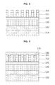
- FIG. 1 is a cross-sectional view illustrating the structure of a multi-luminous element in accordance with an embodiment of the present invention.
- FIGS. 2 to 4 are cross-sectional views illustrating a process of manufacturing a multi-luminous element in accordance with an embodiment of the present invention.
- FIGS. 5 to 7 are plan views illustrating forms of the patterned first active layer.
- FIG. 1 is a cross-sectional view illustrating the structure of a multi-luminous element in accordance with an embodiment of the present invention.
- the multi-luminous element 100 may include a substrate 110 , a buffer layer 120 , a seed layer 130 , a first type semiconductor layer 140 , a patterned first active layer 152 , a mask pattern 162 , a second active layer 170 , and a second type semiconductor layer 180 .
- the multi-luminous element 100 may not have the seed layer 130 or the mask pattern 162 .
- the substrate 110 may be Al 2 O 3 substrate, Si substrate, SiC substrate, GaAs substrate, or sapphire substrate, and may be preferably sapphire substrate.
- the buffer layer 120 may be located between the substrate 110 and the seed layer 130 or the first type semiconductor layer 140 in order to reduce a difference in lattice constant or in coefficient of thermal expansion with an upper layer. Therefore, the buffer layer 120 may be formed of any material capable of reducing a difference in lattice constant or in coefficient of thermal expansion, preferably including AlN or GaN.
- the seed layer 130 may be located on the buffer layer 120 .
- the seed layer 130 may be ⁇ -GaN layer, which may be formed of undopped GaN.
- the first type semiconductor layer 140 may be located on the buffer layer 120 or on the seed layer 130 .
- the first type semiconductor layer 140 may be a semiconductor layer including nitride, for example, including GaN, Al x Ga 1-x N(0 ⁇ x ⁇ 1), In x Ga 1-x N(0 ⁇ x ⁇ 1), or In x Al y Ga 1-(x+y) N(0 ⁇ x ⁇ 1, 0 ⁇ y ⁇ 1, x+y ⁇ 1), preferably including GaN.
- GaN may be N-type GaN doped with N-type impurities, especially N-type GaN ohmic contact layer doped with Si.
- the patterned first active layer 152 may have a quantum well structure, preferably a multiple quantum wells (MQWs) structure. Namely, the patterned first active layer 152 includes at least one barrier layer (not shown) and at least one well layer (not shown), which may be stacked by turns. The patterned first active layer 152 is formed to expose a part of the first type semiconductor layer 140 .
- MQWs multiple quantum wells
- the barrier layer of the patterned first active layer 152 may include Al x1 Ga 1-x1-y1 In 1-x1 N(0 ⁇ x1 ⁇ 1, 0 ⁇ y1 ⁇ 1, x1+y1 ⁇ 1), and the well layer of the patterned first active layer 152 may include Al x2 Ga 1-x2-y2 In 1-x2 N(0 ⁇ x2 ⁇ 1, 0 ⁇ y2 ⁇ 1, x2+y2 ⁇ 1, x2 ⁇ x1, y2 ⁇ y1).
- the barrier layer of the patterned first active layer 152 may be formed with a thickness of 5 to 15 nm, and the well layer of the patterned first active layer 152 may be formed with a thickness of 1 to 3 nm.
- the mask pattern 162 may be located on the patterned first active layer 152 .
- the mask pattern 162 may be formed of any material capable of producing a pattern, preferably formed of SiO 2 , with a thickness of 50 to 200 nm, preferably with a thickness of 100 nm.
- the mask pattern 162 is used as a mask for forming the patterned first active layer 152 , so that the shape of the patterned first active layer 152 may be determined depending on the mask pattern 162 . As shown in FIGS.
- the mask pattern 162 may be formed with one of a linear type pattern 162 a having a specific width in a plan view, a circular type pattern 162 b having a specific diameter in a plan view, and a polygonal type pattern such as a rectangular type pattern 162 c having a specific breadth in a plan view. Therefore, the first active layer 152 may be patterned to expose a part of the underlying first type semiconductor layer 140 in the form of a linear type having a specific width, a circular type having a specific diameter, or a polygonal type such as a rectangular type having a specific breadth, in a plan view.
- the patterned first active layer 152 may be formed with patterns having a width, diameter or breadth between 10 nm and 10 ⁇ m, which may be determined depending on the first wavelength of light emitted from the first active layer 152 .
- This width, diameter or breadth of the patterned first active layer 152 may be determined to satisfy a specific condition ⁇ 1 /4n 1 .
- ⁇ 1 denotes the first wavelength of light emitted from the patterned first active layer 152
- n 1 means a refractive index of the patterned first active layer 152 .
- the width, diameter or breadth of the patterned first active layer 152 may be 500 nm/(4 ⁇ 2.5), i.e., 50 nm.
- the second active layer 170 may be located on the first type semiconductor layer 140 , more exactly, on a part of the first type semiconductor layer 140 exposed by the patterned first active layer 152 .
- the second active layer 170 and the patterned first active layer 152 may be located side by side and repeatedly disposed in a horizontal direction.
- the second active layer 170 may be divided into at least two sections by the patterned first active layer 152 , and adjacent two sections of the second active layer 170 may be separated by the patterned first active layer 152 . That is to say, the patterned first active layer 152 may also be divided into at least two sections by the second active layer 170 , and adjacent two sections of the patterned first active layer 152 may be separated by the second active layer 170 .
- the second active layer 170 may have a quantum well structure, preferably a multiple quantum wells (MQWs) structure. Namely, the second active layer 170 includes at least one barrier layer (not shown) and at least one well layer (not shown), which may be stacked by turns.
- the barrier layer of the second active layer 170 may include Al x3 Ga 1-x3-y3 In 1-x3 N(0 ⁇ x3 ⁇ 1, 0 ⁇ y3 ⁇ 1, x3+y3 ⁇ 1), and the well layer of the second active layer 170 may include Al x4 Ga 1-x4-y4 In 1-x4 N(0 ⁇ x4 ⁇ 1, 0 ⁇ y4 ⁇ 1, x4+y4 ⁇ 1, x4 ⁇ x3, y4 ⁇ y3).
- the barrier layer of the second active layer 170 may be formed with a thickness of 5 to 15 nm, and the well layer of the second active layer 170 may be formed with a thickness of 1 to 3 nm.
- the second active layer 170 may be formed with patterns having a width, diameter or breadth between 10 nm and 10 ⁇ m, which may be determined depending on the second wavelength of light emitted from the second active layer 170 .
- This width, diameter or breadth of the second active layer 170 may be determined to satisfy a specific condition ⁇ 2 /4n 2 .
- ⁇ 2 denotes the second wavelength of light emitted from the second active layer 170
- n 2 means a refractive index of the second active layer 170 .
- the width, diameter or breadth of the second active layer 170 may be 300 nm/(4 ⁇ 2.5), i.e., 30 nm.
- the second active layer 170 may emit light having the second wavelength which is different from the wavelength of light emitted from the patterned first active layer 152 .
- the first and second active layers 152 and 170 may emit light with the first wavelength and light with the second wavelength, respectively, by varying the ratio of Al to In or Ga.
- the ratio of Al increases in comparison with the ratio of In or Ga, the wavelength of light emitted is decreased. Therefore, in order for the patterned first active layer 152 to emit light having a longer wavelength in comparison with the second active layer 170 , the patterned first active layer 152 may be formed to have a lower ratio of In or Ga to Al in comparison with the second active layer 170 .
- the second type semiconductor layer 180 may be a semiconductor layer including nitride, for example, including GaN, Al x Ga 1-x N(0 ⁇ x ⁇ 1), In x Ga 1-x N(0 ⁇ x ⁇ 1), or In x Al y Ga 1-(x+y) N(0 ⁇ x ⁇ 1, 0 ⁇ y ⁇ 1, x+y ⁇ 1), preferably including GaN.
- GaN may be P-type GaN ohmic contact layer doped with P-type impurities.
- the second type semiconductor layer 180 may be located on the patterned first active layer 152 and the second active layer 170 .
- the mask pattern 162 may be interposed between the second type semiconductor layer 180 and the patterned first active layer 152 . If the mask pattern 162 is not included, the second type semiconductor layer 180 may be in a direct contact with both of the patterned first active layer 152 and the second active layer 170 .
- An electrical connection, i.e., a flow of current, among the first type semiconductor layer 140 , the patterned first active layer 152 , the second active layer 170 , and the second type semiconductor layer 180 may vary depending on whether the mask pattern 162 is included or not. If the mask pattern 162 is not existent, there are three paths, namely, a path connected by the first type semiconductor layer 140 , the patterned first active layer 152 , and the second type semiconductor layer 180 , a path connected by the first type semiconductor layer 140 , the second active layer 170 , and the second type semiconductor layer 180 , and a path connected by the first type semiconductor layer 140 , the patterned first active layer 152 , the second active layer 170 , and the second type semiconductor layer 180 .
- the mask pattern 162 acts as an insulating layer and thus there are two paths, namely, a path connected by the first type semiconductor layer 140 , the second active layer 170 , and the second type semiconductor layer 180 , and a path connected by the first type semiconductor layer 140 , the patterned first active layer 152 , the second active layer 170 , and the second type semiconductor layer 180 .
- the multi-luminous element 100 of an embodiment has the advantage of capability to produce multi-wavelength without loss of luminous efficiency.
- each of the patterned first active layer 152 and the second active layer 170 may be formed with a quantum well structure.
- light emitted in a vertical direction from the patterned first active layer 152 advances in an upward or downward direction of the multi-luminous element 100 .
- light emitted in a horizontal direction, namely emitted laterally, from the patterned first active layer 152 advances in other form.
- light emitted laterally from the patterned first active layer 152 meets a surface of the second active layer 170 on a transmission path of light.
- the patterned first active layer 152 and the second active layer 170 have different refractive indexes due to different ratios of constituents. Therefore, light emitted from the patterned first active layer 152 is refracted or reflected at the surface of the second active layer 170 .
- the width, diameter or breadth of the patterned first active layer 152 satisfies a specific condition ⁇ 1 /4n 1 as discussed above, laterally transmitted light from the patterned first active layer 152 is amplified. As a result, the light extraction efficiency of the patterned first active layer 152 is enhanced.
- the second active layer 170 The same applies to the second active layer 170 . Specifically, light emitted in a vertical direction from the second active layer 170 advances in an upward or downward direction of the multi-luminous element 100 , and light emitted from the second active layer 170 is refracted or reflected at the surface of the patterned first active layer 152 . Since the width, diameter or breadth of the second active layer 170 satisfies a specific condition ⁇ 2 /4n 2 as discussed above, laterally transmitted light from the second active layer 170 is amplified. As a result, the light extraction efficiency of the second active layer 170 is enhanced.
- the multi-luminous element 100 of an embodiment may extract light with various colors. Namely, depending on the first wavelength of light emitted from the patterned first active layer 152 and the second wavelength of light emitted from the second active layer 170 , the multi-luminous element 100 may extract light having various colors such as red, green or blue and also extract white light or other light such as ultraviolet light or infrared light. This extraction of light having various wavelengths may cause the possibility of being applied to various fields.
- the multi-luminous element 100 is used as a light source for the growth of plants
- light having a wavelength corresponding to blue (Blue light is believed to promote the formation of leaves of plants.) may be extracted from the patterned first active layer 152
- light having a wavelength corresponding to red (Red light is believed to promote photosynthesis.) or light having a wavelength corresponding to ultraviolet (UV light is believed to make the leaves of plants thick or to promote the color formation of pigment.) may be extracted from the second active layer 170 .
- the patterned first active layer 152 may have the well layer composed of 2% Al, 76% Ga, and 22% In so as to extract light with 460 nm wavelength corresponding to blue.
- the second active layer 170 may have the well layer composed of 0.5% Al, 49.5% Ga, and 50% In so as to extract red light with 650 nm wavelength or have the well layer composed of 6% Al, 86% Ga, and 8% In so as to extract UV light with 380 nm wavelength.
- the patterned first active layer 152 may extract yellow light and the second active layer 170 may extract blue light.
- the patterned first active layer 152 may have 0.8% Al, 59.2% Ga, and 40% In so as to extract yellow light
- the second active layer 170 may have 2% Al, 76% Ga, and 22% In so as to extract blue light.
- the multi-luminous element 100 includes two active layers only, it is possible to have three or more active layers which emit light with different wavelengths.
- FIGS. 2 to 4 are cross-sectional views illustrating a process of manufacturing a multi-luminous element in accordance with an embodiment of the present invention.
- FIGS. 5 to 7 are plan views illustrating forms of the patterned first active layer.
- a method for manufacturing a multi-luminous element begins with preparing the substrate 110 .
- the substrate 110 may be Al 2 O 3 substrate, Si substrate, SiC substrate, GaAs substrate, or sapphire substrate, and may be preferably sapphire substrate (Al 2 O 3 substrate).
- the buffer layer 120 , the seed layer 130 , the first type semiconductor layer 140 , a first active layer 150 , and a mask layer 160 are sequentially stacked on the substrate 110 .
- Each of the buffer layer 120 , the seed layer 130 , the first type semiconductor layer 140 , the first active layer 150 , and the mask layer 160 may be formed using physical vapor deposition or chemical vapor deposition such as sputtering, PECVD (Plasma Enhanced Chemical Vapor Deposition), MOCVD (Metal Organic Chemical Vapor Deposition), ALD (Atomic Layer Deposition), MBE (Molecular Beam Epitaxy), and HVPE (Hybrid Vapor Phase Epitaxy).
- physical vapor deposition or chemical vapor deposition such as sputtering, PECVD (Plasma Enhanced Chemical Vapor Deposition), MOCVD (Metal Organic Chemical Vapor Deposition), ALD (Atomic Layer Deposition), MBE (Molecular Beam Epitaxy), and HVPE (Hybrid Vapor Phase Epitaxy).
- the buffer layer 120 may be formed of nitride including AlN or GaN, and the seed layer 130 may be formed of undopped ⁇ -GaN.
- the first type semiconductor layer 140 may be a semiconductor layer including nitride, for example, including GaN, Al x Ga 1-x N(0 ⁇ x ⁇ 1), In x Ga 1-x N(0 ⁇ x ⁇ 1), or In x Al y Ga 1-(x+y) N(0 ⁇ x ⁇ 1, 0 ⁇ y ⁇ 1, x+y ⁇ 1), preferably including GaN.
- GaN may be N-type GaN doped with N-type impurities, especially N-type GaN ohmic contact layer doped with Si.
- the first active layer 150 is formed by stacking at least one barrier layer with 5 to 15 nm thickness and at least one well layer with 1 to 3 nm thickness.
- the barrier layer may be composed of Al x1 Ga 1-x1-y1 In 1-x1 N(0 ⁇ x1 ⁇ 1, 0 ⁇ y1 ⁇ 1, x1+y1 ⁇ 1), and the well layer may be composed of Al x2 Ga 1-x2-y2 In 1-x2 N(0 ⁇ x2 ⁇ 1, 0 ⁇ y2 ⁇ 1, x2+y2 ⁇ 1, x2 ⁇ x1, y2 ⁇ y1).
- the mask layer 160 may be formed of any material capable of producing a pattern, preferably formed of SiO 2 , with a thickness of 50 to 200 nm, preferably 100 nm thickness.
- the buffer layer 120 is formed in a temperature atmosphere of 450 to 600° C.
- the first type semiconductor layer 140 is formed in a temperature atmosphere of 1000 to 1100° C.
- the first active layer 150 is formed in a temperature atmosphere of 700 to 850° C.
- the mask pattern 162 is formed from the mask layer 160 .
- the mask pattern 162 may be formed to have at least one of a linear type pattern 162 a having a specific width in a plan view, a circular type pattern 162 b having a specific diameter in a plan view, and a polygonal type pattern such as a rectangular type pattern 162 c having a specific breadth in a plan view in order to expose a part of the underlying first type semiconductor layer 140 .
- the mask pattern 162 is formed to have a width, diameter or breadth between 10 nm and 10 ⁇ m.
- the patterned first active layer 152 is formed. Namely, the first active layer 150 is etched to expose a part of the first type semiconductor layer 140 , thus forming the patterned first active layer 152 .
- a dry etching which is an anisotropic etching is used.
- the second active layer 170 is formed over the substrate 110 having the patterned first active layer 150 .
- the second active layer 170 is formed by stacking at least one barrier layer with 5 to 15 nm thickness and at least one well layer with 1 to 3 nm thickness.
- the barrier layer may be composed of Al x3 Ga 1-x3-y3 In 1-x3 N(0 ⁇ x3 ⁇ 1, 0 ⁇ y3 ⁇ 1, x3+y3 ⁇ 1)
- the well layer may be composed of Al x4 Ga 1-x4-y4 In 1-x4 N(0 ⁇ x4 ⁇ 1, 0 ⁇ y4 ⁇ 1, x4+y4 ⁇ 1, x4 ⁇ x3, y4 ⁇ y3).
- the second active layer 170 may be formed in a temperature atmosphere of 700 to 850° C.
- the second active layer 170 may be formed through growth using epitaxial growth technique or the like on a part of the first type semiconductor layer 140 exposed by the patterned first active layer 152 .
- the second active layer 170 is not formed on the mask pattern 162 since the growth of the second active layer 170 is not permitted on the mask pattern 162 .
- the second active layer 170 may be formed through vapor deposition technique using organic metal such as MOCVD over the substrate 110 having the patterned first active layer 152 .
- the second active layer 170 may be formed on the mask pattern 162 as well as on the first type semiconductor layer 140 exposed by the patterned first active layer 152 . Therefore, the second active layer 170 formed on the mask pattern 162 is removed through wet etching using BOE (Buffer Oxide Etchant) and HF solution or through equipment for planarization such as CMP (Chemical Mechanical Planarization).
- BOE Buffer Oxide Etchant
- CMP Chemical Mechanical Planarization
- the mask pattern 162 may be removed.
- the patterned first active layer 152 and the second active layer 170 are formed using the mask pattern 162 .
- three or more active layers may be formed using two or more mask patterns.
- the second type semiconductor layer 180 is formed over the substrate 110 having the patterned first active layer 152 and the second active layer 170 .
- the multi-luminous element according to an embodiment is obtained.
- the second type semiconductor layer 180 may be formed in a temperature atmosphere of 1000 to 1100° C.
- the second type semiconductor layer 180 may be a semiconductor layer including nitride, for example, including GaN, Al x Ga 1-x N(0 ⁇ x ⁇ 1), In x Ga 1-x N(0 ⁇ x ⁇ 1), or In x Al y Ga 1-(x+y) N(0 ⁇ x ⁇ 1, 0 ⁇ y ⁇ 1, x+y ⁇ 1), preferably including GaN.
- GaN may be P-type GaN ohmic contact layer doped with P-type impurities.
Applications Claiming Priority (3)
| Application Number | Priority Date | Filing Date | Title |
|---|---|---|---|
| KR10-2010-0023611 | 2010-03-17 | ||
| KR1020100023611A KR101122020B1 (ko) | 2010-03-17 | 2010-03-17 | 다중발광소자 및 이를 제조하는 방법 |
| PCT/KR2011/001813 WO2011115414A2 (ko) | 2010-03-17 | 2011-03-15 | 다중발광소자 및 이를 제조하는 방법 |
Related Parent Applications (1)
| Application Number | Title | Priority Date | Filing Date |
|---|---|---|---|
| PCT/KR2011/001813 A-371-Of-International WO2011115414A2 (ko) | 2010-03-17 | 2011-03-15 | 다중발광소자 및 이를 제조하는 방법 |
Related Child Applications (1)
| Application Number | Title | Priority Date | Filing Date |
|---|---|---|---|
| US14/277,905 Division US9508897B2 (en) | 2010-03-17 | 2014-05-15 | Multi-luminous element and method for manufacturing same |
Publications (2)
| Publication Number | Publication Date |
|---|---|
| US20120319081A1 US20120319081A1 (en) | 2012-12-20 |
| US8765505B2 true US8765505B2 (en) | 2014-07-01 |
Family
ID=44649716
Family Applications (2)
| Application Number | Title | Priority Date | Filing Date |
|---|---|---|---|
| US13/581,399 Active US8765505B2 (en) | 2010-03-17 | 2011-03-15 | Multi-luminous element and method for manufacturing same |
| US14/277,905 Active US9508897B2 (en) | 2010-03-17 | 2014-05-15 | Multi-luminous element and method for manufacturing same |
Family Applications After (1)
| Application Number | Title | Priority Date | Filing Date |
|---|---|---|---|
| US14/277,905 Active US9508897B2 (en) | 2010-03-17 | 2014-05-15 | Multi-luminous element and method for manufacturing same |
Country Status (3)
| Country | Link |
|---|---|
| US (2) | US8765505B2 (ko) |
| KR (1) | KR101122020B1 (ko) |
| WO (1) | WO2011115414A2 (ko) |
Families Citing this family (3)
| Publication number | Priority date | Publication date | Assignee | Title |
|---|---|---|---|---|
| KR101981119B1 (ko) * | 2011-11-25 | 2019-05-22 | 엘지이노텍 주식회사 | 자외선 반도체 발광 소자 |
| DE102013112490A1 (de) * | 2013-11-13 | 2015-05-13 | Osram Opto Semiconductors Gmbh | Halbleiterschichtenfolge und Verfahren zu deren Herstellung |
| JP6077076B1 (ja) * | 2015-09-11 | 2017-02-08 | 株式会社東芝 | グラフェン配線構造及びグラフェン配線構造の作製方法 |
Citations (15)
| Publication number | Priority date | Publication date | Assignee | Title |
|---|---|---|---|---|
| JPH0955538A (ja) | 1995-08-10 | 1997-02-25 | Furukawa Electric Co Ltd:The | 多波長発光素子 |
| JPH11233816A (ja) | 1998-02-13 | 1999-08-27 | Oki Electric Ind Co Ltd | 半導体発光装置およびその製造方法 |
| US20020053681A1 (en) * | 1998-03-11 | 2002-05-09 | Kabushiki Kaisha Toshiba | Semiconductor light emitting element |
| US20020139984A1 (en) * | 2001-01-26 | 2002-10-03 | Kabushiki Kaisha Toshiba | Semiconductor light emitting element |
| US20030138983A1 (en) * | 2002-01-17 | 2003-07-24 | Goshi Biwa | Selective growth method, and semiconductor light emitting device and fabrication method thereof |
| US20040195598A1 (en) * | 2000-10-23 | 2004-10-07 | Tysoe Steven Alfred | Light-based system for detecting analytes |
| US20050161683A1 (en) * | 2003-06-24 | 2005-07-28 | Samsung Electro-Mechanics Co., Ltd. | White light emitting diode and method for manufacturing the same |
| US20050194598A1 (en) * | 2004-02-13 | 2005-09-08 | Hwa-Mok Kim | Super bright light emitting diode of nanorod array structure having InGaN quantum well and method for manufacturing the same |
| KR100699147B1 (ko) | 2005-12-15 | 2007-03-21 | 엘지전자 주식회사 | 다파장 발광소자 및 그 제조방법 |
| US20070085095A1 (en) * | 2005-10-17 | 2007-04-19 | Samsung Electro-Mechanics Co., Ltd. | Nitride based semiconductor light emitting diode |
| US20070221932A1 (en) * | 2006-03-22 | 2007-09-27 | Sanyo Electric Co., Ltd. | Method of fabricating nitride-based semiconductor light-emitting device and nitride-based semiconductor light-emitting device |
| US20080124824A1 (en) * | 2006-11-28 | 2008-05-29 | National Taiwan University | Method for forming electronic devices by using protecting layers |
| US20080308820A1 (en) * | 2007-06-15 | 2008-12-18 | Tpo Displays Corp. | Light-Emitting Diode Arrays and Methods of Manufacture |
| US20100051977A1 (en) * | 2006-12-18 | 2010-03-04 | Seoul Opto Device Co., Ltd. | Light emitting device having isolating insulative layer for isolating light emitting cells from each other and method of fabricating the same |
| US20100197060A1 (en) * | 2009-02-05 | 2010-08-05 | Chun-Yen Chang | Method of Forming Laterally Distributed LEDs |
Family Cites Families (8)
| Publication number | Priority date | Publication date | Assignee | Title |
|---|---|---|---|---|
| JPH0255538A (ja) | 1988-08-20 | 1990-02-23 | Fujitsu Ltd | 直流給電方法 |
| WO2000030178A1 (en) * | 1998-11-16 | 2000-05-25 | Emcore Corporation | Iii-nitride quantum well structures with indium-rich clusters and methods of making the same |
| DE10032246A1 (de) * | 2000-07-03 | 2002-01-17 | Osram Opto Semiconductors Gmbh | Lumineszenzdiodenchip auf der Basis von InGaN und Verfahren zu dessen Herstellung |
| TW586246B (en) * | 2002-10-28 | 2004-05-01 | Super Nova Optoelectronics Cor | Manufacturing method of white light LED and the light-emitting device thereof |
| JP2005072323A (ja) | 2003-08-26 | 2005-03-17 | Oki Data Corp | 半導体装置 |
| EP1958257A2 (en) * | 2005-11-24 | 2008-08-20 | Koninklijke Philips Electronics N.V. | Light emitting diode construction |
| US20100148147A1 (en) * | 2008-12-17 | 2010-06-17 | Palo Alto Research Center Incorporated | Monolithic white and full-color light emitting diodes using selective area growth |
| TWI397989B (zh) * | 2009-12-07 | 2013-06-01 | Epistar Corp | 發光二極體陣列 |
-
2010
- 2010-03-17 KR KR1020100023611A patent/KR101122020B1/ko active IP Right Grant
-
2011
- 2011-03-15 US US13/581,399 patent/US8765505B2/en active Active
- 2011-03-15 WO PCT/KR2011/001813 patent/WO2011115414A2/ko active Application Filing
-
2014
- 2014-05-15 US US14/277,905 patent/US9508897B2/en active Active
Patent Citations (15)
| Publication number | Priority date | Publication date | Assignee | Title |
|---|---|---|---|---|
| JPH0955538A (ja) | 1995-08-10 | 1997-02-25 | Furukawa Electric Co Ltd:The | 多波長発光素子 |
| JPH11233816A (ja) | 1998-02-13 | 1999-08-27 | Oki Electric Ind Co Ltd | 半導体発光装置およびその製造方法 |
| US20020053681A1 (en) * | 1998-03-11 | 2002-05-09 | Kabushiki Kaisha Toshiba | Semiconductor light emitting element |
| US20040195598A1 (en) * | 2000-10-23 | 2004-10-07 | Tysoe Steven Alfred | Light-based system for detecting analytes |
| US20020139984A1 (en) * | 2001-01-26 | 2002-10-03 | Kabushiki Kaisha Toshiba | Semiconductor light emitting element |
| US20030138983A1 (en) * | 2002-01-17 | 2003-07-24 | Goshi Biwa | Selective growth method, and semiconductor light emitting device and fabrication method thereof |
| US20050161683A1 (en) * | 2003-06-24 | 2005-07-28 | Samsung Electro-Mechanics Co., Ltd. | White light emitting diode and method for manufacturing the same |
| US20050194598A1 (en) * | 2004-02-13 | 2005-09-08 | Hwa-Mok Kim | Super bright light emitting diode of nanorod array structure having InGaN quantum well and method for manufacturing the same |
| US20070085095A1 (en) * | 2005-10-17 | 2007-04-19 | Samsung Electro-Mechanics Co., Ltd. | Nitride based semiconductor light emitting diode |
| KR100699147B1 (ko) | 2005-12-15 | 2007-03-21 | 엘지전자 주식회사 | 다파장 발광소자 및 그 제조방법 |
| US20070221932A1 (en) * | 2006-03-22 | 2007-09-27 | Sanyo Electric Co., Ltd. | Method of fabricating nitride-based semiconductor light-emitting device and nitride-based semiconductor light-emitting device |
| US20080124824A1 (en) * | 2006-11-28 | 2008-05-29 | National Taiwan University | Method for forming electronic devices by using protecting layers |
| US20100051977A1 (en) * | 2006-12-18 | 2010-03-04 | Seoul Opto Device Co., Ltd. | Light emitting device having isolating insulative layer for isolating light emitting cells from each other and method of fabricating the same |
| US20080308820A1 (en) * | 2007-06-15 | 2008-12-18 | Tpo Displays Corp. | Light-Emitting Diode Arrays and Methods of Manufacture |
| US20100197060A1 (en) * | 2009-02-05 | 2010-08-05 | Chun-Yen Chang | Method of Forming Laterally Distributed LEDs |
Non-Patent Citations (1)
| Title |
|---|
| International Search Report mailed Oct. 31, 2011 for PCT/KR2011/001813. |
Also Published As
| Publication number | Publication date |
|---|---|
| KR101122020B1 (ko) | 2012-03-09 |
| WO2011115414A3 (ko) | 2011-12-29 |
| US9508897B2 (en) | 2016-11-29 |
| US20140246649A1 (en) | 2014-09-04 |
| US20120319081A1 (en) | 2012-12-20 |
| WO2011115414A2 (ko) | 2011-09-22 |
| KR20110104627A (ko) | 2011-09-23 |
Similar Documents
| Publication | Publication Date | Title |
|---|---|---|
| JP4359263B2 (ja) | 半導体発光装置 | |
| US9373755B2 (en) | Light-emitting diodes on concave texture substrate | |
| KR101891777B1 (ko) | 유전체 리플렉터를 구비한 발광소자 및 그 제조방법 | |
| US8853671B2 (en) | Nanorod light emitting device and method of manufacturing the same | |
| US9166105B2 (en) | Light emitting device | |
| KR101452801B1 (ko) | 발광다이오드 및 이의 제조방법 | |
| CN110416249A (zh) | 一种半导体发光器件及其制作方法 | |
| US20220278165A1 (en) | Led arrays | |
| US20120161185A1 (en) | Light emitting diodes | |
| JP2007123731A (ja) | 半導体発光素子および半導体発光装置 | |
| KR20090101604A (ko) | 그룹 3족 질화물계 반도체 발광다이오드 소자 및 이의 제조방법 | |
| US9508897B2 (en) | Multi-luminous element and method for manufacturing same | |
| US20120074379A1 (en) | Light-emitting element and the manufacturing method thereof | |
| KR20130099574A (ko) | 질화갈륨 기판을 갖는 발광 다이오드 | |
| KR101862407B1 (ko) | 질화물계 반도체 발광소자 및 그 제조방법 | |
| KR101582330B1 (ko) | 나노 발광다이오드 또는 마이크로 발광다이오드 구조 및 이의 제조방법 | |
| KR100604562B1 (ko) | 발광 다이오드 및 그 제조방법 | |
| KR20230060507A (ko) | Led 디바이스 및 led 디바이스를 제조하는 방법 | |
| KR20220162167A (ko) | 알루미늄 함유층을 내부에 포함하는 발광 다이오드 및 이와 관련한 방법 | |
| JP4995432B2 (ja) | 半導体発光装置 | |
| CN114424350A (zh) | 发光二极管阵列 | |
| KR20130101299A (ko) | 반도체 발광소자 및 그 제조 방법 | |
| CN213366616U (zh) | 微型发光二极管阵列 | |
| KR20090065052A (ko) | 질화물 반도체 발광소자 및 그 제조 방법 | |
| KR20130098761A (ko) | 질화갈륨 기판을 갖는 발광 다이오드 |
Legal Events
| Date | Code | Title | Description |
|---|---|---|---|
| AS | Assignment |
Owner name: KOREA PHOTONICS TECHNOLOGY INSTITUTE, KOREA, REPUB Free format text: ASSIGNMENT OF ASSIGNORS INTEREST;ASSIGNORS:JEON, SEONG RAN;KIM, JAE BUM;LEE, SEUNG JAE;SIGNING DATES FROM 20120817 TO 20120820;REEL/FRAME:028852/0720 |
|
| STCF | Information on status: patent grant |
Free format text: PATENTED CASE |
|
| MAFP | Maintenance fee payment |
Free format text: PAYMENT OF MAINTENANCE FEE, 4TH YR, SMALL ENTITY (ORIGINAL EVENT CODE: M2551) Year of fee payment: 4 |
|
| MAFP | Maintenance fee payment |
Free format text: PAYMENT OF MAINTENANCE FEE, 8TH YR, SMALL ENTITY (ORIGINAL EVENT CODE: M2552); ENTITY STATUS OF PATENT OWNER: SMALL ENTITY Year of fee payment: 8 |