US8759845B2 - Semiconductor light emitting device utilising punch-through effects - Google Patents
Semiconductor light emitting device utilising punch-through effects Download PDFInfo
- Publication number
- US8759845B2 US8759845B2 US12/863,743 US86374309A US8759845B2 US 8759845 B2 US8759845 B2 US 8759845B2 US 86374309 A US86374309 A US 86374309A US 8759845 B2 US8759845 B2 US 8759845B2
- Authority
- US
- United States
- Prior art keywords
- region
- junction
- junction region
- depletion
- light emitting
- Prior art date
- Legal status (The legal status is an assumption and is not a legal conclusion. Google has not performed a legal analysis and makes no representation as to the accuracy of the status listed.)
- Expired - Fee Related, expires
Links
Images


Classifications
-
- H—ELECTRICITY
- H10—SEMICONDUCTOR DEVICES; ELECTRIC SOLID-STATE DEVICES NOT OTHERWISE PROVIDED FOR
- H10H—INORGANIC LIGHT-EMITTING SEMICONDUCTOR DEVICES HAVING POTENTIAL BARRIERS
- H10H20/00—Individual inorganic light-emitting semiconductor devices having potential barriers, e.g. light-emitting diodes [LED]
- H10H20/80—Constructional details
- H10H20/81—Bodies
- H10H20/813—Bodies having a plurality of light-emitting regions, e.g. multi-junction LEDs or light-emitting devices having photoluminescent regions within the bodies
-
- H—ELECTRICITY
- H10—SEMICONDUCTOR DEVICES; ELECTRIC SOLID-STATE DEVICES NOT OTHERWISE PROVIDED FOR
- H10H—INORGANIC LIGHT-EMITTING SEMICONDUCTOR DEVICES HAVING POTENTIAL BARRIERS
- H10H20/00—Individual inorganic light-emitting semiconductor devices having potential barriers, e.g. light-emitting diodes [LED]
- H10H20/80—Constructional details
- H10H20/81—Bodies
- H10H20/822—Materials of the light-emitting regions
- H10H20/826—Materials of the light-emitting regions comprising only Group IV materials
Definitions
- This invention relates to optoelectronic devices and more particularly to a light emitting device fabricated from a semiconductor material and to a method of generating light in a semiconductor material.
- Avalanche electroluminescent light emission in single crystal indirect bandgap semiconductors is generated by the interaction between mobile carriers (e.g. recombination of electrons and holes) and lattice phonons in a reverse biased pn junction.
- the internal quantum efficiency (number of photons generated per electron) can be enhanced if “cool” (low energy) carriers are injected into the reverse biased junction from a closely spaced forward biased junction to interact with the “hot” energetic carriers within the depletion region.
- the carriers injected from the forward biased junction will be injected across all of the forward biased junction area (sidewalls and bottom wall). This means that only a relatively small percentage of all the injected carriers reach the reverse biased depletion region, to initiate light generation. The carriers not reaching the reverse biased avalanching depletion are lost and represent device current not being utilized for light generation, thus reducing the power efficiency of the light source.
- a light emitting device comprising;
- the semiconductor material may be an indirect bandgap material. Alternatively it may be a direct bandgap material.
- the breakthrough mode may be an avalanche mode, alternatively a field emission mode, further alternatively a combination of avalanche and field emission.
- the first doping kind may be n and the second doping kind may be p. In other embodiments the first doping kind may be p and the second doping kind may be n.
- the first depletion region may punch through to the second junction region.
- the terminal arrangement may comprise two terminals, a first terminal connected to the first region of the body, to apply a voltage of a first polarity to the first region; and a second terminal connected to the third region of the body, to apply a voltage of an opposite polarity to the third region.
- the terminal arrangement may comprise three terminals, a first terminal connected to the first region of the body; a second terminal connected to the third region of the body; and a third terminal connected to the second region of the body.
- a modulation signal may be applied to the third terminal.
- the first and second terminals may be used for controlling electroluminescence processes, carrier energies and carrier density profiles; and the third terminal may be used for controlling the modulation of the output electroluminescence of the device.
- the invention further includes in its scope a method of operating a light emitting device comprising the steps of:
- the second junction may be slightly reverse biased and the first part of the second junction region may be caused to be forward biased by the punched through first depletion region.
- FIG. 1 is a diagrammatic representation of a silicon light emitting device
- FIG. 2 is a schematic diagram of the layout in plan of a conventional silicon carrier injection light emitting device
- FIG. 3 is a schematic section on line III in FIG. 2 ;
- FIG. 4 is a energy band diagram for the conventional device in FIGS. 2 and 3 ;
- FIG. 5 is a diagram similar to FIG. 2 for the device in accordance with the invention.
- FIG. 6 is an energy band diagram for the carrier injection device in accordance with the invention.
- FIG. 7 is a diagrammatic representation of a two terminal device in accordance with the invention.
- FIG. 8 is a diagram of carrier concentration profiles in a conventional n + p diode
- FIG. 9 is a similar diagram in a punch through n + pn + device in accordance with the invention.
- FIG. 10 is a schematic diagram of an alternative embodiment of the device according to the invention.
- FIG. 11 is a diagram of electrical field strength and distribution of the device in FIG. 10 ;
- FIG. 12 is an alternative representation of the device in FIG. 10 ;
- FIG. 13 is a diagrammatic representation of carrier energy against distance for the device in FIG. 10 ;
- FIG. 14 is a diagram of carrier concentration against distance for the device in FIG. 10 ;
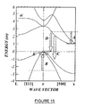
- FIG. 15 is a Si band diagram illustrating possible and different photonic energy transitions.
- a multi-terminal light emitting device fabricated from a semiconductor material is generally designated by the reference numeral 10 in FIG. 1 .
- the material may be an indirect bandgap semiconductor material, such as Si, Ge and Si—Ge. In other embodiments, a direct bandgap material may be used.
- the device 10 comprises a body 12 of an indirect bandgap semiconductor material, in this case Si.
- the body comprises a first junction region 14 between a first region 12 . 1 of the body of a first doping kind and a second region 12 . 2 of the first body of a second doping kind.
- the first body further comprises a second junction region 16 between the second region 12 . 2 and a third region 12 . 3 of the body, also of the first doping kind.
- the first doping kind may be n + and the second doping kind may be p. In other embodiments opposite doping kinds may be used.
- a terminal arrangement 18 is connected to the body for, in use, reverse biasing the first junction region 14 into a breakdown mode and for forward biasing at least part of the second junction region 16 , to inject carriers towards the first junction region.
- the breakdown mode may be an avalanche mode, alternatively a field emission mode, further alternatively a combination of avalanche and field emission.
- the device 10 is configured so that a first depletion region 20 associated with the reverse biased first junction region 14 punches through to a second depletion region associated with the forward biased second junction region 16 .
- the first depletion region 20 punches through to at least first part 16 . 1 of the second junction region 16 .
- the energy diagram shown in FIG. 4 presents the energy barriers of the two junctions 114 and 116 in a conventional device 100 as shown in FIGS. 2 and 3 .
- the barrier of the reverse biased junction 114 is increased from the equilibrium condition, while the barriers of the forward biased junction 116 is reduced compared to the equilibrium (zero volt bias) condition.
- the width of depletion region 120 of the reversed bias junction 114 is indicated at 122 and the energy barrier of the forward biased junction 116 is indicated at 124 in FIG. 4 .
- the energy barrier 24 at the forward biased junction is even further lowered by the encroaching depletion region 20 from the reverse biased junction 14 .
- This effect is commonly known as punch through, normally seen as a negative parasitic effect, but in this case the effect is used in a positive way to enhance avalanche electroluminescence effects.
- the punch through effect can be localised as shown at 16 . 1 in FIG. 5 .
- the reverse biased junction depletion region 20 punches through to the laterally spaced nearby junction 16 in a localized, well defined, part or interface 16 . 1 .
- the nearby junction energy barrier 24 is lowered locally at the intersection interface 16 . 1 , causing that part 16 . 1 of the junction 16 to be more forward biased than the rest of the junction area.
- the nearby junction 16 can in fact be slightly reverse biased to stop carrier injection entirely across all of the nearby junction area.
- the punch through interface 16 . 1 will be the only part of the nearby junction being forward biased by the energy barrier lowering effect, causing exclusive carrier injection into the reverse biased junction depletion region. it is believed that by using the device in this mode, there may be less losses as a result of carrier injection into the bulk not reaching the reverse biased depletion region, and it is further believed that electroluminescence efficiency may be improved.
- the carrier injection punch through device 10 in accordance with the invention may also be operated as a two terminal device. In this mode of operation, the p-type bulk contact of the terminal arrangement 18 is not necessary.
- the carrier concentration profile for the conventional n + p junction in avalanche breakdown is shown in FIG. 8 and the carrier concentration profile for the punch through n + pn + structure is shown in FIG. 9 .
- the device represented in FIG. 8 has a relatively wide depletion region, high avalanche gain and low electron carrier concentration on the depletion region edge next to the p-region.
- the carriers to be avalanche multiplied are thermally generated in the p-region, and constitute a small thermally generated leakage current.
- the avalanche gain must be high to increase this small leakage current to a relatively large reverse avalanche current to generate light.
- the current to be avalanche multiplied is the injection current from the forward biased junction 16 , which is much higher than the thermally generated leakage current.
- the avalanche gain needed should be less to attain the same light generating current, causing the depletion region 20 to be narrower, resulting in shorter transit time of carriers through the device 10 and thus faster switching response.
- the narrower depletion region 20 may also result in a lower operating voltage, resulting in improved power efficiency of the light generating process.
- Another advantage of the punch through device 10 may be that at the point of carrier injection form the forward biased junction 16 , i.e. near the forward biased junction, large numbers of “cool” (low energy) electrons are in the same volume region of the depletion region 20 with large numbers of accelerated “hot” (energetic) holes, which will enhance the radiative direct bandgap carrier recombination process.
- FIG. 10 there is shown a diagrammatic representation of an alternative device according to the invention in the form of a p + np + avalanche injection silicon electroluminescent device 10 .
- FIG. 11 a diagram of electrical field strength and distribution through the device 10 is given. Near a first p + n junction 14 the electric filed conditions reach high enough magnitudes to allow ionization and multiplication of host atoms. This region is referred to as the excitation zone. Because of the ionization of host atoms in the centre n region, the electric field strength gradually decays until it reaches the second p+n junction 16 . The region between the two junctions is referred to as the drift zone 30 .
- the remaining short electric field decay is taken up by ionization of host dopant atoms in the highly doped p + region 12 . 3 . Because of the specific bias conditions and as illustrated in FIG. 12 , a large density of low energy (cool) holes is injected from the second p + n junction 16 , also referred to as the injection zone, into the drift zone 30 .
- a distribution of both excited high energy electrons is formed at the excitation junction 14 .
- These electrons traverse through the drift zone 30 of the device. During their traverse they may interact with defect centers that may act as recombination or relaxation centers. Since large densities of holes are injected from the injection zone 16 and which travel in a direction opposite to that of the electrons, recombination may occur between high energy drifting electrons and lower energy injected holes in the whole of the drift zone 30 .
- FIG. 13 Representations of carrier energy for both electrons and holes as they traverse the drift region 30 are shown in FIG. 13 .
- Excited electrons traverse through the drift zone 30 substantially maintaining their maximum ionization energy for host atoms, which is approximately 1.8 eV.
- the electric field strength is high enough to sustain this energy for the electrons throughout the drift region.
- punch through interface the interface where the depletion region 20 and injecting junction depletion region meet
- the holes being injected into the drift zone from the injecting p + n junction gain energy fast and it is assumed that they gain maximum ionization energy for holes of host silicon of approximately 2.3 eV within 150 to 200 nm.
- the holes maintain their energy as they traverse the rest of the drift zone 30 . Recombination processes between high energy electrons and medium and high energy holes may occur throughout the drift zone, but may have minor implication on the energy and carrier distribution.
- FIG. 14 shows the corresponding projected carrier density profiles for electrons and holes as they traverse the drift zone 30 .
- the electrons traverse the zone with high speed (near saturation velocity), without much decrease in carrier density.
- their concentration may rapidly decay until all electrons has recombined with holes. This process may occur mainly in the last part of the drift zone 30 and even into the neutral p + region.
- high densities of low energy holes are injected from the junction 16 and interact with the traversing high energy exiting electrons. It can hence be assumed that the hole concentration rapidly decays from the junction 16 to certain moderate levels.
Landscapes
- Led Devices (AREA)
Applications Claiming Priority (3)
| Application Number | Priority Date | Filing Date | Title |
|---|---|---|---|
| ZA200800593 | 2008-01-21 | ||
| ZA2008/00593 | 2008-01-21 | ||
| PCT/IB2009/050209 WO2009093177A1 (en) | 2008-01-21 | 2009-01-21 | Semiconductor light emitting device utilising punch-through effects |
Publications (2)
| Publication Number | Publication Date |
|---|---|
| US20110031893A1 US20110031893A1 (en) | 2011-02-10 |
| US8759845B2 true US8759845B2 (en) | 2014-06-24 |
Family
ID=40586889
Family Applications (1)
| Application Number | Title | Priority Date | Filing Date |
|---|---|---|---|
| US12/863,743 Expired - Fee Related US8759845B2 (en) | 2008-01-21 | 2009-01-21 | Semiconductor light emitting device utilising punch-through effects |
Country Status (5)
| Country | Link |
|---|---|
| US (1) | US8759845B2 (enExample) |
| EP (1) | EP2245676A1 (enExample) |
| JP (1) | JP5676273B2 (enExample) |
| WO (1) | WO2009093177A1 (enExample) |
| ZA (1) | ZA201004753B (enExample) |
Families Citing this family (8)
| Publication number | Priority date | Publication date | Assignee | Title |
|---|---|---|---|---|
| JP5550558B2 (ja) * | 2007-11-01 | 2014-07-16 | インシアヴァ (ピーテーワイ) リミテッド | 光誘導機構を有するオプトエレクトロニック・デバイスおよびその機構を形成する方法 |
| WO2009093177A1 (en) | 2008-01-21 | 2009-07-30 | Insiava (Pty) Limited | Semiconductor light emitting device utilising punch-through effects |
| CN101933169B (zh) * | 2008-02-01 | 2012-07-11 | Insiava(控股)有限公司 | 包括异质结的半导体发光器件 |
| CN102292834A (zh) | 2008-12-15 | 2011-12-21 | 因西亚瓦(控股)有限公司 | 利用穿通效应的硅发光器件 |
| EP2526571B1 (en) | 2010-01-22 | 2019-05-01 | Insiava (Pty) Limited | Silicon light emitting device and method of fabricating same |
| JP5665504B2 (ja) * | 2010-11-24 | 2015-02-04 | キヤノン株式会社 | 垂直共振器型面発光レーザおよび垂直共振器型面発光レーザアレイ |
| EP2756527B1 (en) | 2011-09-16 | 2015-11-18 | Insiava (Pty) Limited | Near infrared light source in bulk silicon |
| US20210280736A1 (en) * | 2016-09-06 | 2021-09-09 | University Of South Africa | OPTIMISED 650 nm SILICON AVALANCHE LED |
Citations (14)
| Publication number | Priority date | Publication date | Assignee | Title |
|---|---|---|---|---|
| JPS60167390A (ja) | 1984-02-09 | 1985-08-30 | Matsushita Electric Ind Co Ltd | 半導体発光素子 |
| EP0276140A2 (en) | 1987-01-23 | 1988-07-27 | Hiroshima University | A light emitting semiconductor device |
| US5136353A (en) * | 1990-05-10 | 1992-08-04 | The University Of Colorado Foundation, Inc. | Optical switch |
| US5510627A (en) * | 1994-06-29 | 1996-04-23 | The United States Of America As Represented By The Secretary Of The Navy | Infrared-to-visible converter |
| US5994720A (en) | 1996-03-04 | 1999-11-30 | University Of Pretoria | Indirect bandgap semiconductor optoelectronic device |
| US6111271A (en) * | 1996-03-28 | 2000-08-29 | University Of Pretoria | Optoelectronic device with separately controllable carrier injection means |
| US6365911B1 (en) | 1999-07-23 | 2002-04-02 | Kabushiki Kaisha Toshiba | Bidirectional semiconductor light-emitting element and optical system |
| WO2005020287A2 (en) | 2003-08-22 | 2005-03-03 | The Board Of Trustees Of The University Of Illinois | Semiconductor device and method |
| WO2009047716A1 (en) | 2007-10-08 | 2009-04-16 | Insiava (Pty) Limited | Silicon light emitting device with carrier injection |
| US20110042701A1 (en) | 2007-11-01 | 2011-02-24 | Monuko Du Plessis | Optoelectronic device with light directing arrangement and method of forming the arrangement |
| US20110068716A1 (en) | 2008-02-01 | 2011-03-24 | Lukas Willem Snyman | Semiconductor light emitting device comprising heterojunction |
| US20120001681A1 (en) | 2008-12-15 | 2012-01-05 | Monuko Du Plessis | Light emitting device with encapsulated reach-through region |
| US20130026534A1 (en) | 2010-01-22 | 2013-01-31 | Insiava (Pty) Limited | Silicon light emitting device and method of fabricating same |
| US8395226B2 (en) | 2009-01-27 | 2013-03-12 | Insiava (Pty) Limited | Microchip-based MOEMS and waveguide device |
Family Cites Families (2)
| Publication number | Priority date | Publication date | Assignee | Title |
|---|---|---|---|---|
| JP2002246639A (ja) * | 2001-02-20 | 2002-08-30 | Fujitsu Ltd | 半導体発光装置 |
| WO2009093177A1 (en) | 2008-01-21 | 2009-07-30 | Insiava (Pty) Limited | Semiconductor light emitting device utilising punch-through effects |
-
2009
- 2009-01-21 WO PCT/IB2009/050209 patent/WO2009093177A1/en not_active Ceased
- 2009-01-21 US US12/863,743 patent/US8759845B2/en not_active Expired - Fee Related
- 2009-01-21 EP EP09703175A patent/EP2245676A1/en not_active Ceased
- 2009-01-21 JP JP2010543598A patent/JP5676273B2/ja not_active Expired - Fee Related
-
2010
- 2010-07-06 ZA ZA2010/04753A patent/ZA201004753B/en unknown
Patent Citations (16)
| Publication number | Priority date | Publication date | Assignee | Title |
|---|---|---|---|---|
| JPS60167390A (ja) | 1984-02-09 | 1985-08-30 | Matsushita Electric Ind Co Ltd | 半導体発光素子 |
| EP0276140A2 (en) | 1987-01-23 | 1988-07-27 | Hiroshima University | A light emitting semiconductor device |
| US5136353A (en) * | 1990-05-10 | 1992-08-04 | The University Of Colorado Foundation, Inc. | Optical switch |
| US5510627A (en) * | 1994-06-29 | 1996-04-23 | The United States Of America As Represented By The Secretary Of The Navy | Infrared-to-visible converter |
| US5994720A (en) | 1996-03-04 | 1999-11-30 | University Of Pretoria | Indirect bandgap semiconductor optoelectronic device |
| US6111271A (en) * | 1996-03-28 | 2000-08-29 | University Of Pretoria | Optoelectronic device with separately controllable carrier injection means |
| US6365911B1 (en) | 1999-07-23 | 2002-04-02 | Kabushiki Kaisha Toshiba | Bidirectional semiconductor light-emitting element and optical system |
| WO2005020287A2 (en) | 2003-08-22 | 2005-03-03 | The Board Of Trustees Of The University Of Illinois | Semiconductor device and method |
| WO2009047716A1 (en) | 2007-10-08 | 2009-04-16 | Insiava (Pty) Limited | Silicon light emitting device with carrier injection |
| US8362679B2 (en) | 2007-10-08 | 2013-01-29 | Insiava (Pty) Limited | Silicon light emitting device with carrier injection |
| US20110042701A1 (en) | 2007-11-01 | 2011-02-24 | Monuko Du Plessis | Optoelectronic device with light directing arrangement and method of forming the arrangement |
| US20110068716A1 (en) | 2008-02-01 | 2011-03-24 | Lukas Willem Snyman | Semiconductor light emitting device comprising heterojunction |
| US20120001681A1 (en) | 2008-12-15 | 2012-01-05 | Monuko Du Plessis | Light emitting device with encapsulated reach-through region |
| US20120009709A1 (en) | 2008-12-15 | 2012-01-12 | Monuko Du Plessis | Silicon light emitting device utilising reach-through effects |
| US8395226B2 (en) | 2009-01-27 | 2013-03-12 | Insiava (Pty) Limited | Microchip-based MOEMS and waveguide device |
| US20130026534A1 (en) | 2010-01-22 | 2013-01-31 | Insiava (Pty) Limited | Silicon light emitting device and method of fabricating same |
Non-Patent Citations (12)
| Title |
|---|
| Corrected Version of International Preliminary Report on Patentability for PCT/IB2009/050209, completed May 3, 2010. (stamp receipt date Jul. 21, 2010). |
| Du Plessis et al., "Two- and Multi-terminal CMOS/BiCMOS LED's", Publishers B.V. Amsterdam, NL vol. 27, No. 5, Feb. 1, 2005, pp. 1059-1063, XP025328182. |
| Snyman at al., "Increasing the Efficiency of p <+>np<+> Injection-avalanche Si CMOS LED's (450 nm-750 nm) by means of Depletion Layer Profiling and Reach-through Techniques", Proceedings of SPIE Silicon Photonics III, vol. 6898, Feb. 7, 2008, pp. 68980E-1-68980E-12, XP002527052. |
| Snyman at al., "Increasing the Efficiency of p np Injection-avalanche Si CMOS LED's (450 nm-750 nm) by means of Depletion Layer Profiling and Reach-through Techniques", Proceedings of SPIE Silicon Photonics III, vol. 6898, Feb. 7, 2008, pp. 68980E-1-68980E-12, XP002527052. |
| Snyman et al., "Injection-avalanche-based n<+>pn Silicon Complementary Metal-Oxide-Semiconductor light-emitting device (450-750 nm) with 2-order-of-magnitude Increase in Light Emission Intensity", Japanese Journal of Applied Physics, Part 1 (Regular Papers, Short Notes & Review Papers) Japan Society of Applied Physics Through the Institute of Pure and Applied Physics Japan, vol. 46, No. 48, Apr. 2007, pp. 2474-2480, XP002527051. |
| Snyman et al., "Injection-avalanche-based npn Silicon Complementary Metal-Oxide-Semiconductor light-emitting device (450-750 nm) with 2-order-of-magnitude Increase in Light Emission Intensity", Japanese Journal of Applied Physics, Part 1 (Regular Papers, Short Notes & Review Papers) Japan Society of Applied Physics Through the Institute of Pure and Applied Physics Japan, vol. 46, No. 48, Apr. 2007, pp. 2474-2480, XP002527051. |
| U.S. Appl. No. 12/740,597 (Du Plessis et al.) filed Oct. 20, 2010. |
| U.S. Appl. No. 12/865,609 (Snyman et al.) filed Jul. 30, 2010 (now allowed). |
| U.S. Appl. No. 13/139,653 (Du Plessis) filed Jun. 14, 2011. |
| U.S. Appl. No. 13/161,113 (Du Plessis) filed Jun. 15, 2011. |
| U.S. Appl. No. 13/574,333 (Venter, Petrus Johannes) filed Jul. 20, 2012. |
| U.S. Appl. No. 13/810,809 (Du Plessis et al.) filed Apr. 1, 2013. |
Also Published As
| Publication number | Publication date |
|---|---|
| WO2009093177A1 (en) | 2009-07-30 |
| JP5676273B2 (ja) | 2015-02-25 |
| EP2245676A1 (en) | 2010-11-03 |
| ZA201004753B (en) | 2011-08-31 |
| US20110031893A1 (en) | 2011-02-10 |
| JP2011510511A (ja) | 2011-03-31 |
Similar Documents
| Publication | Publication Date | Title |
|---|---|---|
| US8759845B2 (en) | Semiconductor light emitting device utilising punch-through effects | |
| US9306113B2 (en) | Silicon light emitting device utilising reach-through effects | |
| US8362679B2 (en) | Silicon light emitting device with carrier injection | |
| US8674382B2 (en) | Semiconductor light emitting device comprising heterojunction | |
| US7977693B2 (en) | Semiconductor light-emitting material with tetrahedral structure formed therein | |
| EP2919282B1 (en) | Nitride semiconductor stacked body and semiconductor light emitting device comprising the same | |
| US7821019B2 (en) | Triple heterostructure incorporating a strained zinc oxide layer for emitting light at high temperatures | |
| Slipchenko et al. | Model of steady-state injection processes in a high-power laser-thyristor based on heterostructure with internal optical feedback | |
| Gupta et al. | Electron-hole bilayer light-emitting device: concept and operation | |
| JP2015163693A (ja) | 発光材料、発光材料の製造方法、発光素子、及び発光デバイス | |
| Shmagin et al. | Effect of space charge region width on er-related luminescence in reverse biased Si: Er-based light emitting diodes | |
| Zavada et al. | Efficient nitride-based short-wavelength emitters with enhanced hole injection | |
| WO2009093170A1 (en) | Silicon light emitting device utilising reach-through effects | |
| Manyakhin et al. | Avalanche breakdown luminescence of InGaN/AlGaN/GaN heterostructures | |
| RU2576345C2 (ru) | Излучающая гетероструктура с внутренним усилением инжекции | |
| du Plessis et al. | Silicon-on-insulator (SOI) nanowire hot carrier electroluminescence | |
| Schubert et al. | GaN Light-Emitting Triodes (LETs) for High-Efficiency Hole Injection and for Assessment of the Physical Origin of the Efficiency Droop | |
| Kornaukhov et al. | On the nature of electroluminescence at 1.5 μm in the breakdown mode of reverse-biased Er-doped silicon pn-junction structures grown by sublimation molecular beam epitaxy |
Legal Events
| Date | Code | Title | Description |
|---|---|---|---|
| AS | Assignment |
Owner name: INSIAVA (PTY) LIMITED, SOUTH AFRICA Free format text: ASSIGNMENT OF ASSIGNORS INTEREST;ASSIGNORS:SNYMAN, LUKAS WILLEM;DU PLESSIS, MONUKO;SIGNING DATES FROM 20100729 TO 20101018;REEL/FRAME:025153/0162 |
|
| STCF | Information on status: patent grant |
Free format text: PATENTED CASE |
|
| FEPP | Fee payment procedure |
Free format text: ENTITY STATUS SET TO SMALL (ORIGINAL EVENT CODE: SMAL) |
|
| MAFP | Maintenance fee payment |
Free format text: PAYMENT OF MAINTENANCE FEE, 4TH YR, SMALL ENTITY (ORIGINAL EVENT CODE: M2551) Year of fee payment: 4 |
|
| FEPP | Fee payment procedure |
Free format text: MAINTENANCE FEE REMINDER MAILED (ORIGINAL EVENT CODE: REM.); ENTITY STATUS OF PATENT OWNER: SMALL ENTITY |
|
| LAPS | Lapse for failure to pay maintenance fees |
Free format text: PATENT EXPIRED FOR FAILURE TO PAY MAINTENANCE FEES (ORIGINAL EVENT CODE: EXP.); ENTITY STATUS OF PATENT OWNER: SMALL ENTITY |
|
| STCH | Information on status: patent discontinuation |
Free format text: PATENT EXPIRED DUE TO NONPAYMENT OF MAINTENANCE FEES UNDER 37 CFR 1.362 |
|
| FP | Lapsed due to failure to pay maintenance fee |
Effective date: 20220624 |