US8747177B2 - Light-emitting display and method of manufacturing the same - Google Patents
Light-emitting display and method of manufacturing the same Download PDFInfo
- Publication number
- US8747177B2 US8747177B2 US13/765,406 US201313765406A US8747177B2 US 8747177 B2 US8747177 B2 US 8747177B2 US 201313765406 A US201313765406 A US 201313765406A US 8747177 B2 US8747177 B2 US 8747177B2
- Authority
- US
- United States
- Prior art keywords
- layer
- electrode
- aperture
- forming
- light
- Prior art date
- Legal status (The legal status is an assumption and is not a legal conclusion. Google has not performed a legal analysis and makes no representation as to the accuracy of the status listed.)
- Active
Links
- 238000004519 manufacturing process Methods 0.000 title claims description 24
- 239000000463 material Substances 0.000 claims description 66
- 238000005530 etching Methods 0.000 claims description 49
- 238000000034 method Methods 0.000 claims description 39
- 239000000758 substrate Substances 0.000 claims description 22
- 238000000059 patterning Methods 0.000 claims description 9
- 239000010410 layer Substances 0.000 description 171
- 239000010408 film Substances 0.000 description 111
- 238000005401 electroluminescence Methods 0.000 description 76
- 239000010409 thin film Substances 0.000 description 29
- 229910052751 metal Inorganic materials 0.000 description 28
- 239000002184 metal Substances 0.000 description 28
- 239000010936 titanium Substances 0.000 description 19
- 238000007789 sealing Methods 0.000 description 10
- 238000000206 photolithography Methods 0.000 description 9
- 239000011347 resin Substances 0.000 description 9
- 229920005989 resin Polymers 0.000 description 9
- 238000002161 passivation Methods 0.000 description 8
- 230000001681 protective effect Effects 0.000 description 8
- 229910045601 alloy Inorganic materials 0.000 description 7
- 239000000956 alloy Substances 0.000 description 7
- 238000000605 extraction Methods 0.000 description 7
- 239000011159 matrix material Substances 0.000 description 7
- QTBSBXVTEAMEQO-UHFFFAOYSA-N Acetic acid Chemical compound CC(O)=O QTBSBXVTEAMEQO-UHFFFAOYSA-N 0.000 description 6
- 230000000052 comparative effect Effects 0.000 description 6
- 230000004048 modification Effects 0.000 description 6
- 238000012986 modification Methods 0.000 description 6
- 239000011810 insulating material Substances 0.000 description 5
- 238000001020 plasma etching Methods 0.000 description 5
- NBIIXXVUZAFLBC-UHFFFAOYSA-N Phosphoric acid Chemical compound OP(O)(O)=O NBIIXXVUZAFLBC-UHFFFAOYSA-N 0.000 description 4
- VYPSYNLAJGMNEJ-UHFFFAOYSA-N Silicium dioxide Chemical compound O=[Si]=O VYPSYNLAJGMNEJ-UHFFFAOYSA-N 0.000 description 4
- XUIMIQQOPSSXEZ-UHFFFAOYSA-N Silicon Chemical compound [Si] XUIMIQQOPSSXEZ-UHFFFAOYSA-N 0.000 description 4
- 229910052782 aluminium Inorganic materials 0.000 description 4
- 239000004020 conductor Substances 0.000 description 4
- 229910052710 silicon Inorganic materials 0.000 description 4
- 239000010703 silicon Substances 0.000 description 4
- 238000004544 sputter deposition Methods 0.000 description 4
- 238000001039 wet etching Methods 0.000 description 4
- 238000005229 chemical vapour deposition Methods 0.000 description 3
- 239000010949 copper Substances 0.000 description 3
- 230000000694 effects Effects 0.000 description 3
- 239000011777 magnesium Substances 0.000 description 3
- 239000007769 metal material Substances 0.000 description 3
- BASFCYQUMIYNBI-UHFFFAOYSA-N platinum Chemical compound [Pt] BASFCYQUMIYNBI-UHFFFAOYSA-N 0.000 description 3
- 229910052719 titanium Inorganic materials 0.000 description 3
- GRYLNZFGIOXLOG-UHFFFAOYSA-N Nitric acid Chemical compound O[N+]([O-])=O GRYLNZFGIOXLOG-UHFFFAOYSA-N 0.000 description 2
- 229910004541 SiN Inorganic materials 0.000 description 2
- 239000002253 acid Substances 0.000 description 2
- XAGFODPZIPBFFR-UHFFFAOYSA-N aluminium Chemical compound [Al] XAGFODPZIPBFFR-UHFFFAOYSA-N 0.000 description 2
- 229910000147 aluminium phosphate Inorganic materials 0.000 description 2
- 239000011651 chromium Substances 0.000 description 2
- 239000011248 coating agent Substances 0.000 description 2
- 238000000576 coating method Methods 0.000 description 2
- 229910052681 coesite Inorganic materials 0.000 description 2
- 229910052802 copper Inorganic materials 0.000 description 2
- 229910052906 cristobalite Inorganic materials 0.000 description 2
- 230000007423 decrease Effects 0.000 description 2
- 230000007547 defect Effects 0.000 description 2
- 239000010931 gold Substances 0.000 description 2
- 229910052749 magnesium Inorganic materials 0.000 description 2
- 229910052750 molybdenum Inorganic materials 0.000 description 2
- 229910017604 nitric acid Inorganic materials 0.000 description 2
- 238000007254 oxidation reaction Methods 0.000 description 2
- 229920002120 photoresistant polymer Polymers 0.000 description 2
- 229920001721 polyimide Polymers 0.000 description 2
- 239000009719 polyimide resin Substances 0.000 description 2
- 239000000377 silicon dioxide Substances 0.000 description 2
- 229910052814 silicon oxide Inorganic materials 0.000 description 2
- 229910052709 silver Inorganic materials 0.000 description 2
- 229910052682 stishovite Inorganic materials 0.000 description 2
- 238000010301 surface-oxidation reaction Methods 0.000 description 2
- 239000012780 transparent material Substances 0.000 description 2
- 229910052905 tridymite Inorganic materials 0.000 description 2
- 238000001771 vacuum deposition Methods 0.000 description 2
- 239000004925 Acrylic resin Substances 0.000 description 1
- 229920000178 Acrylic resin Polymers 0.000 description 1
- 229910001316 Ag alloy Inorganic materials 0.000 description 1
- 229910000838 Al alloy Inorganic materials 0.000 description 1
- 229910000789 Aluminium-silicon alloy Inorganic materials 0.000 description 1
- 229910052684 Cerium Inorganic materials 0.000 description 1
- VYZAMTAEIAYCRO-UHFFFAOYSA-N Chromium Chemical compound [Cr] VYZAMTAEIAYCRO-UHFFFAOYSA-N 0.000 description 1
- RYGMFSIKBFXOCR-UHFFFAOYSA-N Copper Chemical compound [Cu] RYGMFSIKBFXOCR-UHFFFAOYSA-N 0.000 description 1
- FYYHWMGAXLPEAU-UHFFFAOYSA-N Magnesium Chemical compound [Mg] FYYHWMGAXLPEAU-UHFFFAOYSA-N 0.000 description 1
- ZOKXTWBITQBERF-UHFFFAOYSA-N Molybdenum Chemical compound [Mo] ZOKXTWBITQBERF-UHFFFAOYSA-N 0.000 description 1
- 229910052779 Neodymium Inorganic materials 0.000 description 1
- BQCADISMDOOEFD-UHFFFAOYSA-N Silver Chemical compound [Ag] BQCADISMDOOEFD-UHFFFAOYSA-N 0.000 description 1
- RTAQQCXQSZGOHL-UHFFFAOYSA-N Titanium Chemical compound [Ti] RTAQQCXQSZGOHL-UHFFFAOYSA-N 0.000 description 1
- NRTOMJZYCJJWKI-UHFFFAOYSA-N Titanium nitride Chemical compound [Ti]#N NRTOMJZYCJJWKI-UHFFFAOYSA-N 0.000 description 1
- 239000012790 adhesive layer Substances 0.000 description 1
- 229910021417 amorphous silicon Inorganic materials 0.000 description 1
- 230000005540 biological transmission Effects 0.000 description 1
- 230000015572 biosynthetic process Effects 0.000 description 1
- GWXLDORMOJMVQZ-UHFFFAOYSA-N cerium Chemical compound [Ce] GWXLDORMOJMVQZ-UHFFFAOYSA-N 0.000 description 1
- 229910052804 chromium Inorganic materials 0.000 description 1
- 238000007796 conventional method Methods 0.000 description 1
- 238000010304 firing Methods 0.000 description 1
- 239000011521 glass Substances 0.000 description 1
- PCHJSUWPFVWCPO-UHFFFAOYSA-N gold Chemical compound [Au] PCHJSUWPFVWCPO-UHFFFAOYSA-N 0.000 description 1
- 229910052737 gold Inorganic materials 0.000 description 1
- 230000005525 hole transport Effects 0.000 description 1
- AMGQUBHHOARCQH-UHFFFAOYSA-N indium;oxotin Chemical compound [In].[Sn]=O AMGQUBHHOARCQH-UHFFFAOYSA-N 0.000 description 1
- 239000011733 molybdenum Substances 0.000 description 1
- QEFYFXOXNSNQGX-UHFFFAOYSA-N neodymium atom Chemical compound [Nd] QEFYFXOXNSNQGX-UHFFFAOYSA-N 0.000 description 1
- 229920003986 novolac Polymers 0.000 description 1
- 239000004033 plastic Substances 0.000 description 1
- 229920003023 plastic Polymers 0.000 description 1
- 229910052697 platinum Inorganic materials 0.000 description 1
- 229920002577 polybenzoxazole Polymers 0.000 description 1
- 230000006798 recombination Effects 0.000 description 1
- 238000005215 recombination Methods 0.000 description 1
- 238000002310 reflectometry Methods 0.000 description 1
- 239000004332 silver Substances 0.000 description 1
- 239000010944 silver (metal) Substances 0.000 description 1
- 239000002356 single layer Substances 0.000 description 1
- WFKWXMTUELFFGS-UHFFFAOYSA-N tungsten Chemical compound [W] WFKWXMTUELFFGS-UHFFFAOYSA-N 0.000 description 1
- 229910052721 tungsten Inorganic materials 0.000 description 1
- 239000010937 tungsten Substances 0.000 description 1
- YVTHLONGBIQYBO-UHFFFAOYSA-N zinc indium(3+) oxygen(2-) Chemical compound [O--].[Zn++].[In+3] YVTHLONGBIQYBO-UHFFFAOYSA-N 0.000 description 1
Images


Classifications
-
- H—ELECTRICITY
- H01—ELECTRIC ELEMENTS
- H01L—SEMICONDUCTOR DEVICES NOT COVERED BY CLASS H10
- H01L21/00—Processes or apparatus adapted for the manufacture or treatment of semiconductor or solid state devices or of parts thereof
- H01L21/02—Manufacture or treatment of semiconductor devices or of parts thereof
- H01L21/04—Manufacture or treatment of semiconductor devices or of parts thereof the devices having at least one potential-jump barrier or surface barrier, e.g. PN junction, depletion layer or carrier concentration layer
- H01L21/18—Manufacture or treatment of semiconductor devices or of parts thereof the devices having at least one potential-jump barrier or surface barrier, e.g. PN junction, depletion layer or carrier concentration layer the devices having semiconductor bodies comprising elements of Group IV of the Periodic System or AIIIBV compounds with or without impurities, e.g. doping materials
- H01L21/30—Treatment of semiconductor bodies using processes or apparatus not provided for in groups H01L21/20 - H01L21/26
- H01L21/31—Treatment of semiconductor bodies using processes or apparatus not provided for in groups H01L21/20 - H01L21/26 to form insulating layers thereon, e.g. for masking or by using photolithographic techniques; After treatment of these layers; Selection of materials for these layers
- H01L21/3105—After-treatment
- H01L21/31051—Planarisation of the insulating layers
-
- H—ELECTRICITY
- H05—ELECTRIC TECHNIQUES NOT OTHERWISE PROVIDED FOR
- H05B—ELECTRIC HEATING; ELECTRIC LIGHT SOURCES NOT OTHERWISE PROVIDED FOR; CIRCUIT ARRANGEMENTS FOR ELECTRIC LIGHT SOURCES, IN GENERAL
- H05B33/00—Electroluminescent light sources
- H05B33/10—Apparatus or processes specially adapted to the manufacture of electroluminescent light sources
-
- H—ELECTRICITY
- H10—SEMICONDUCTOR DEVICES; ELECTRIC SOLID-STATE DEVICES NOT OTHERWISE PROVIDED FOR
- H10K—ORGANIC ELECTRIC SOLID-STATE DEVICES
- H10K50/00—Organic light-emitting devices
- H10K50/80—Constructional details
- H10K50/805—Electrodes
- H10K50/81—Anodes
- H10K50/814—Anodes combined with auxiliary electrodes, e.g. ITO layer combined with metal lines
-
- H—ELECTRICITY
- H10—SEMICONDUCTOR DEVICES; ELECTRIC SOLID-STATE DEVICES NOT OTHERWISE PROVIDED FOR
- H10K—ORGANIC ELECTRIC SOLID-STATE DEVICES
- H10K50/00—Organic light-emitting devices
- H10K50/80—Constructional details
- H10K50/805—Electrodes
- H10K50/82—Cathodes
- H10K50/824—Cathodes combined with auxiliary electrodes
-
- H—ELECTRICITY
- H10—SEMICONDUCTOR DEVICES; ELECTRIC SOLID-STATE DEVICES NOT OTHERWISE PROVIDED FOR
- H10K—ORGANIC ELECTRIC SOLID-STATE DEVICES
- H10K59/00—Integrated devices, or assemblies of multiple devices, comprising at least one organic light-emitting element covered by group H10K50/00
- H10K59/10—OLED displays
- H10K59/12—Active-matrix OLED [AMOLED] displays
- H10K59/122—Pixel-defining structures or layers, e.g. banks
-
- H—ELECTRICITY
- H10—SEMICONDUCTOR DEVICES; ELECTRIC SOLID-STATE DEVICES NOT OTHERWISE PROVIDED FOR
- H10K—ORGANIC ELECTRIC SOLID-STATE DEVICES
- H10K59/00—Integrated devices, or assemblies of multiple devices, comprising at least one organic light-emitting element covered by group H10K50/00
- H10K59/10—OLED displays
- H10K59/12—Active-matrix OLED [AMOLED] displays
- H10K59/131—Interconnections, e.g. wiring lines or terminals
- H10K59/1315—Interconnections, e.g. wiring lines or terminals comprising structures specially adapted for lowering the resistance
-
- H—ELECTRICITY
- H10—SEMICONDUCTOR DEVICES; ELECTRIC SOLID-STATE DEVICES NOT OTHERWISE PROVIDED FOR
- H10K—ORGANIC ELECTRIC SOLID-STATE DEVICES
- H10K59/00—Integrated devices, or assemblies of multiple devices, comprising at least one organic light-emitting element covered by group H10K50/00
- H10K59/80—Constructional details
- H10K59/805—Electrodes
- H10K59/8051—Anodes
- H10K59/80516—Anodes combined with auxiliary electrodes, e.g. ITO layer combined with metal lines
-
- H—ELECTRICITY
- H10—SEMICONDUCTOR DEVICES; ELECTRIC SOLID-STATE DEVICES NOT OTHERWISE PROVIDED FOR
- H10K—ORGANIC ELECTRIC SOLID-STATE DEVICES
- H10K59/00—Integrated devices, or assemblies of multiple devices, comprising at least one organic light-emitting element covered by group H10K50/00
- H10K59/80—Constructional details
- H10K59/805—Electrodes
- H10K59/8052—Cathodes
- H10K59/80522—Cathodes combined with auxiliary electrodes
Definitions
- the present invention relates to a top emission system light-emitting display and a method of manufacturing such a light-emitting display.
- organic EL displays displaying an image through the use of an organic EL (Electro Luminescence) phenomenon have received attention.
- the organic EL displays use the light-emitting phenomenon of an organic light-emitting device, so the organic EL displays have superior characteristics such as a wide viewing angle and low power consumption.
- the organic EL displays have high responsivity to a high-definition high-speed video signal, so the organic EL displays has been developed toward practical use specifically in a video field or the like.
- An active matrix type organic EL display includes a drive panel in which an organic EL element including an organic light-emitting layer and a drive element (the above-described thin film transistor) for driving the organic EL display element are arranged, and has a configuration in which the drive panel and a sealing panel are bonded together by an adhesive layer so that the organic EL element is sandwiched between the drive panel and the sealing panel. Moreover, the organic EL element has a configuration in which the organic light-emitting layer is formed between a pair of electrodes.
- an electrode on a light extraction side that is, on the sealing panel side is a common electrode for each organic EL element, and is made of, for example, a light-transmissive conductive material such as ITO (Indium Tin Oxide).
- a light-transmissive conductive material such as ITO (Indium Tin Oxide).
- ITO Indium Tin Oxide
- a voltage applied to the electrode on the light extraction side becomes nonuniform in a plane, so there is an issue that positional variations in light emission luminance among organic EL elements occur, and display quality declines.
- Patent Document 1 discloses a technique in which an auxiliary wiring for being connected to an electrode on a light extraction side is formed of the same material as that of an electrode on a drive panel side in the same layer as the electrode on the drive panel side.
- Patent Document 1 Japanese Unexamined Patent Application Publication No. 2002-318556
- an auxiliary wiring is formed of a material with lower resistivity than that of an electrode on a light extraction side and is connected to the electrode on the light extraction side in such a manner, the above-described in-plane nonuniformity of an electrode voltage can be reduced to some extent.
- a light-emitting display including a plurality of drive elements, and a wiring section electrically connected to the drive elements
- the light-emitting display includes: a plurality of first electrodes formed corresponding to the drive elements, respectively, on the drive elements and the wiring section; a plurality of light emission sections formed on the first electrodes, respectively; a common second electrode formed of a material allowing light from the light emission sections to pass therethrough, and arranged on the plurality of light emission sections; an auxiliary wiring section with lower resistance than that of the second electrode; and a conductive contact section electrically connecting between the second electrode and the auxiliary wiring section.
- the second electrode and the auxiliary wiring are electrically connected to each other through the conductive contact section, so even if the surface of the auxiliary wiring is oxidized, an increase in connection resistance is prevented.
- a method of manufacturing a light-emitting display includes: a step of forming a plurality of drive elements and a wiring section on a substrate, and electrically connecting between the plurality of drive elements and the wiring section; a step of forming a first conductive layer on the drive elements and the wiring section; a step of forming a plurality of first electrodes corresponding to the plurality of drive elements, respectively, as well as an auxiliary wiring section by patterning the first conductive layer; a step of forming a light emission section on each of the first electrodes; a step of forming a common second electrode of a material allowing light from each light emission section to pass therethrough on a plurality of the light emission sections; and a step of forming a conductive contact section, and electrically connecting between the second electrode and the auxiliary wiring section through the contact section, wherein the auxiliary wiring section is formed of a material with lower resistance than that of the second electrode.
- the wiring layer and the contact section be formed by patterning the conductive layer.
- the wiring layer and the contact section can be formed in the same step, so manufacturing steps are simplified.
- the second electrode and the auxiliary wiring are electrically connected to each other through the conductive contact section, so even if the surface of the auxiliary wiring is oxidized, an increase in connection resistance can be prevented. Therefore, irrespective of the configuration of the auxiliary wiring, low power consumption can be maintained, and display quality can be improved.
- FIG. 1 is a plan view showing the configuration of a light-emitting display according to a first embodiment of the invention.
- FIG. 2 is a sectional view showing the configuration of the light-emitting display shown in FIG. 1 .
- FIG. 3(A) and FIG. 3(B) are sectional views showing a part of main steps of a method of manufacturing the light-emitting display shown in FIG. 1 .
- FIG. 4(A) and FIG. 4(B) are sectional views showing a step following FIGS. 3(A) and (B).
- FIG. 5(A) and FIG. 5(B) are sectional views showing a step following FIGS. 4(A) and 4(B) .
- FIG. 6 is a sectional view showing the configuration of a light-emitting display according to a comparative example.
- FIG. 7 is a plot showing a relationship between a current flowing between electrodes and a voltage drop in an auxiliary wiring.
- FIG. 8 is a sectional view showing the configuration of a light-emitting display according to another comparative example.
- FIG. 9 is a sectional view showing the configuration of a light-emitting display according to a second embodiment.
- FIG. 10(A) and FIG. 10(B) are sectional views showing a part of main steps of a method of manufacturing the light-emitting display shown in FIG. 9 .
- FIG. 11(A) and FIG. 11(B) are sectional views showing a step following FIGS. 10(A) and (B).
- FIG. 12(A) and FIG. 12(B) are sectional views showing a step following FIGS. 11(A) and 11(B) .
- FIG. 13(A) and FIG. 13(B) are sectional views showing a step following FIG. 12 .
- FIG. 14 is a sectional view showing the configuration of a light-emitting display according to a third embodiment.
- FIG. 15(A) and FIG. 15(B) are sectional views showing a part of main steps of a method of manufacturing the light-emitting display shown in FIG. 14 .
- FIG. 16(A) and FIG. 16(B) are sectional views showing a step following FIGS. 15(A) and 15(B) .
- FIG. 17(A) and FIG. 17(B) are a sectional views showing a step following FIGS. 16(A) and (B).
- FIG. 18 is a sectional view showing the configuration of a light-emitting display according to a modification example of the third embodiment.
- FIG. 19(A) to FIG. 19(D) are sectional views showing the configuration of a mask used in a method of manufacturing a light-emitting display according to a modification example of the invention.
- FIG. 20 is a sectional view showing the configuration of a light-emitting display according to a modification example of the first embodiment corresponding to the case where the mask shown in FIG. 19 is used.
- FIG. 21 is a sectional view showing the configuration of a light-emitting display according to a modification example of the second embodiment corresponding to the case where the mask shown in FIG. 19 is used.
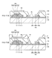
- FIGS. 1 and 2 show the configuration of a light-emitting display (an organic EL display 1 ) according to a first embodiment of the invention, and FIG. 1 shows a plan configuration and FIG. 2 shows a sectional configuration taken along a line II-II of FIG. 1 .
- the organic EL display 1 has a laminate configuration in which a multilayer film is laminated between a pair of insulating transparent substrates 10 A and 10 B. More specifically, a gate electrode 11 , a gate insulating film 12 , a silicon film 13 , a stopper insulating film 14 and a wiring layer 15 A are laminated from the transparent substrate 10 A side to constitute a thin film transistor Tr. Moreover, a passivation insulating film 16 and a planarization insulating film 17 A are laminated on the thin film transistor Tr. On the planarization insulating film 17 A, an organic EL element EL is formed corresponding to a region where the thin film transistor Tr is formed.
- Each organic EL element EL has a laminate configuration in which a first electrode 18 A, an organic light-emitting layer 19 and a second electrode 20 are laminated in order from the planarization insulating film 17 A side.
- the first electrode 18 A and the organic light-emitting layer 19 are separated from other first electrodes 18 A and other light-emitting layers 19 by an interelectrode insulating film 21 on the planarization insulating film 17 A, and the first electrodes 18 A and the organic light-emitting layers 19 both having a rectangular shape shown in, for example, FIG. 2 are arranged in a matrix form between the transparent substrates 10 A and 10 B.
- the second electrode 20 is a common electrode for the organic EL elements EL, and as shown in FIG. 2 , the second electrode 20 is uniformly formed between the transparent substrates 10 A and 10 B.
- an auxiliary wiring 18 B is formed in the same layer as the first electrode 18 A in a region corresponding to a region between the thin film transistors Tr, the first electrodes 18 A and the organic light-emitting layers 19 .
- a forward tapered aperture having a wide top and a narrow bottom is arranged in a part of a region where the auxiliary wiring 18 B is formed (refer to FIG. 1 ).
- a conductive contact section 15 B is formed in the same layer as the wiring layer 15 A, and the second electrode 20 and the auxiliary wiring 18 B are electrically connected to each other on the contact section 15 B.
- a protective film 23 is uniformly formed on the second electrode 20 , and a sealing resin 17 B is uniformly formed between the protective film 23 and the transparent substrate 10 B.
- the transparent substrates 10 A and 10 B are made of, for example, an insulating material such as a glass material or a plastic material.
- the thin film transistor Tr is a drive element for driving each organic EL element EL to emit light.
- the gate electrode 11 is made of, for example, molybdenum (Mo) or the like.
- the silicon film 13 is a section where a channel region of the thin film transistor Tr is formed, and is configured of, for example, an amorphous silicon film or the like.
- the wiring layer 15 A forms a gate electrode and a drain electrode of the thin film transistor Tr, and functions as wiring such as a signal line.
- the wiring layer 15 A is made of the same material as that of the contact section 15 B as will be described later. More specifically, for example, the wiring layer 15 A is made of, for example, a conductive material which is resistant to surface oxidation and establishes a good connection (desirably an ohmic connection) between the wiring layer 15 A and the second electrode 20 . Moreover, as will be described later, a material showing high etching selectivity with respect to the first electrode 18 A is preferable.
- the wiring layer 15 A may be configured of a multilayer film having an uppermost layer made of Ti such as Ti/Al (aluminum), Ti/Al/Ti, Ti/(AlSi alloy), Ti/(AlSiCu alloy), or Ti/(AlCe (cerium) alloy).
- the material of the wiring layer 15 is appropriately selected by the material of the first electrode 18 A, an etching method or the like.
- the passivation insulating film 16 is provided to protect the thin film transistor Tr, and is made of, for example, an insulating material including at least one kind selected from the group consisting of SiO 2 , SiN and SiON.
- the planarization insulating film 17 A is provided to planarize a layer configuration and then form the organic EL element EL on the layer configuration, and is made of, for example, an insulating material such as a photosensitive polyimide resin, a polybenzoxazole resin, a novolac resin, polyhydroxystyrene or an acrylic resin.
- the organic light-emitting layer 19 includes a hole transport layer, a light-emitting layer and an electron transport layer (all not shown) which are deposited in order, and is held between the first electrode 18 A and the second electrode 20 .
- a predetermined voltage is applied between the first electrode 18 A and the second electrode 20 , light emission is obtained by carrier recombination of electrons and holes injected into the light-emitting layer.
- the first electrode 18 A functions as an electrode (an anode electrode or a cathode electrode) for applying a voltage to the organic light-emitting layer 19 as well as a reflecting electrode for reflecting light from the organic light-emitting layer 19 to direct the light upward. Therefore, the first electrode 18 A is made of a metal with high reflectivity, for example, Al, an alloy including Al as a main component such as an AlNd (neodymium) alloy or an AlCe alloy. In addition, such a material of the first electrode 18 A has a property that its surface is easily oxidized (a surface oxidation property).
- the second electrode 20 is also an electrode (an anode electrode or a cathode electrode) for applying a voltage to the organic light-emitting layer 19 .
- the second electrode 20 allows light from the organic light-emitting layer 19 to pass therethrough, and then emits the light upward, so the second electrode 20 is a transparent or semi-transparent electrode. Therefore, the second electrode 20 is made of, for example, ITO or IZO which is a transparent material or a Mg (magnesium)-Ag alloy, Cu, Ag, Mg, Al or the like which is a semi-transparent material.
- the auxiliary wiring 18 B is formed in a region corresponding to a region between the thin film transistors Tr, the first electrodes 18 A and the organic light-emitting layers 19 as described above, and is provided to prevent in-plane nonuniformity of an electrode voltage in the permeable second electrode 20 with high resistance. Therefore, the auxiliary wiring 18 B is configured to have lower resistance than the second electrode 20 (for example, is made of a material with low resistivity), and more specifically, the auxiliary wiring 18 B is made of the same material as the above-described material of the first electrode 18 A.
- the contact section 15 B is provided to establish a partial electrical connection between the second electrode 20 and the auxiliary wiring 18 B, and as described above, the contact section 15 B is formed of the same material as that of the wiring layer 15 A in the same layer as the wiring layer 15 A.
- the contact section 15 B is desirably made of a conductive material which is resistant to surface oxidization and establishes a good connection (desirably an ohmic connection) between the contact section 15 B and the second electrode 20 , more specifically a material showing high etching selectivity with respect to the first electrode 18 A.
- the material showing high etching selectivity with respect to the first electrode 18 A is used, because although the detail will be described later, at the time of forming the first electrode 18 A and the auxiliary wiring 18 B by etching, the contact section 15 B is prevented from being etched together.
- the interelectrode insulating film 21 is provided to separate the organic EL elements EL from one another, and has a side surface with a forward tapered shape having a wide top and a narrow bottom.
- the forward tapered shape preferably has as gentle a tilt angle as possible.
- the width of an aperture in the interelectrode insulating film 21 is larger than that of the aperture in the planarization insulating film 17 A in which the contact section 15 B is formed, and as shown in FIG. 2 , the second electrode 20 has a step-like shape having a wide top and a narrow bottom in these aperture portions.
- the forward tapered shape has as gentle a tilt angle as possible or the aperture portions are formed in a step-like shape to prevent a break or an increase in resistance at the time of forming the second electrode 20 , although the detail will be described later.
- the interelectrode insulating film 21 is made of, for example, an insulating material such as photosensitive polyimide resin.
- the protective film 23 is provided to protect the second electrode 20 , and is made of, for example, an insulating material including at least one kind selected from the group consisting of SiO 2 , SiN and SiON. Moreover, the sealing resin 17 B is provided to planarize a layer configuration and then cover the layer configuration with the transparent substrate 10 B.
- the thin film transistor Tr corresponds to a specific example of “a drive element” in the invention
- the organic light-emitting layer 19 corresponds to a specific example of “a light emission section” in the invention.
- the planarization insulating film 17 A and the interelectrode insulating film 21 correspond to specific examples of “an insulating layer” in the invention.
- FIGS. 3A to 5B show sectional views of a part of steps of manufacturing the organic EL display 1 .
- the gate electrode 11 , the gate insulating film 12 , the silicon film 13 , the stopper insulating film 14 and the wiring layer 15 A which are made of the above-described materials are laminated in this order on the transparent substrate 10 A made of the above-described material by, for example, a sputtering (chemical vapor deposition) method and a photolithography method to form each of a plurality of thin film transistors Tr in, for example, a matrix form on the transparent substrate 10 A.
- the contact section 15 B is also formed of the same material as that of the wiring layer 15 A in a part of a region corresponding to a region between the thin film transistors Tr as shown in FIG. 1 on the gate insulating film 12 , that is, in the same layer as the wiring layer 15 A.
- the passivation insulating film 16 made of the above-described material is uniformly formed on the thin film transistors Tr and the contact section 15 B by, for example, a CVD method.
- the planarization insulating film 17 A made of the above-described material is uniformly formed on the passivation insulating film 16 by coating by, for example, a spin coat method or a slit coat method. Then, a region corresponding to each contact section 15 B is exposed and developed by, for example, a photolithography method to form an aperture, and then firing is performed to form an aperture having a side surface with a forward tapered shape shown in a reference numeral P 1 in the drawing. At this time, as a photosensitive resin used as the planarization insulating film 17 A, such a photosensitive resin that the tilt angle of the aperture becomes as gentle as possible is appropriately selected.
- the aperture may be formed through the use of a halftone mask, or an exposure process may be performed a plurality of times through the use of a plurality of masks having different sizes of aperture portions.
- the tilt angle of the forward tapered shape is appropriately set by the film thickness or the forming method of the second electrode 20 which is formed in a later step.
- the metal layer 18 with a thickness of, for example, approximately 300 nm is uniformly formed of the above-described material of the first electrodes 18 A and the auxiliary wiring 18 B (in this example, a metal material) on the planarization insulating film 17 A and the contact section 15 B by, for example, a sputtering method.
- the metal layer 18 is selectively etched by, for example, a photolithography method to form the first electrodes 18 A and the auxiliary wiring 18 B which have the shapes shown in FIGS. 1 and 2 .
- each first electrode 18 A is formed in a position corresponding to each thin film transistor Tr
- the auxiliary wiring 18 B is formed in a region corresponding to a region between the thin film transistors Tr.
- patterning is performed so that a part of the auxiliary wiring 18 B is electrically connected to the contact section 15 B.
- the contact section 15 B is made of a material with high etching selectivity with respect to the metal layer 18 , so when the metal layer 18 is etched, there is no possibility that the contact section 15 B is etched together with the metal layer 18 .
- etching at this time is performed by wet etching using, for example, a mixed acid including a phosphoric acid, a nitric acid and an acetic acid.
- the interelectrode insulating film 21 made of the above-described material is uniformly formed on the planarization insulating film 17 A, the first electrodes 18 A and the auxiliary wiring 18 B by coating by, for example, a spin coat method or a slit coat method, and patterning is performed on the interelectrode insulating film 21 by, for example, a photolithography method so that a predetermined shape is formed, that is, each first electrode 18 A and each organic light-emitting layer 19 which is formed in a later step are separated from other first electrodes 18 A and other organic light-emitting layers 19 .
- a region corresponding to the contact section 15 B is selectively removed by, for example, a photolithography method to form an aperture having a side surface with a forward tapered shape.
- the aperture may be formed through the use of a halftone mask, or an exposure process may be performed a plurality of times through the use of a plurality of masks having different sizes of aperture portions.
- the width of the aperture in the interelectrode insulating films 21 is configured to be larger than that of the aperture in the planarization insulating film 17 A, and the side surface of the aperture portion is formed in a step-like shape.
- the organic light-emitting layer 19 is formed on each first electrode 18 A by, for example, a vacuum deposition method.
- the second electrode 20 made of the above-described material with a thickness of, for example, approximately 10 nm is uniformly formed on the organic light-emitting layer 19 , the interelectrode insulating film 21 , the planarization insulating film 17 A, the contact section 15 B and the auxiliary wiring 18 B by, for example, a vacuum deposition method.
- the protective film 23 made of the above-described material is uniformly formed on the second electrode 20 by, for example, a CVD method, and the sealing resin 17 B is uniformly formed on the protective film 23 by, for example, an instillation method, and is covered with the transparent substrate 10 B made of the above-described material, thereby the organic EL display 1 according to the embodiment shown in FIGS. 1 and 2 is manufactured.
- the organic light-emitting layer 19 when a voltage is applied to the first electrode 18 A through the wiring layer 15 A and the thin film transistor Tr, the organic light-emitting layer 19 emits light with luminance according to a potential difference between the first electrode 18 A and the second electrode 20 .
- the light from the organic light-emitting layer 19 is reflected by the first electrode 18 A and passes through the second electrode, thereby the light is emitted upward, that is, to the transparent substrate 10 B side in FIG. 2 .
- light on the basis of a pixel signal is emitted from the organic EL element EL arranged in each pixel to display a predetermined image on the organic EL display 1 .
- the second electrode 20 and the auxiliary wiring 18 B are electrically connected to each other through the conductive contact section 15 B which is resistant to surface oxidization and establishes a good connection (desirably an ohmic connection) between the contact section 15 B and the second electrode 20 , so even if the surface of the auxiliary wiring 18 B made of the same material as that of the first electrode 18 A is oxidized, an increase in connection resistance between the second electrode 20 and the auxiliary wiring 18 B is prevented.
- an auxiliary wiring 118 B is formed of the same material as that of a first electrode 118 A in the same layer as the first electrode 118 A, and is directly connected to a second electrode 120 , so when the surface of the auxiliary wiring 118 B is oxidized, connection resistance between the second electrode 120 and the auxiliary wiring 118 B is increased.
- an auxiliary wiring 218 B is formed of the same material as that of the wiring layer 15 A in the same layer as the wiring layer 15 A, so an issue of the above-described increase in connection resistance is prevented; however, it is difficult to form the auxiliary wiring 218 B due to a restriction on layout imposed by the thin film transistor Tr or the wiring layer 15 A. Moreover, even if the auxiliary wiring 218 B can be formed, a distance between wirings is very short, so a short circuit between wirings through the auxiliary wiring 218 B easily occurs, and the yield of the display declines.
- the auxiliary wiring 18 B is formed in the same layer as the first electrode 18 A, and only a part of the auxiliary wiring 18 B positioned in a region corresponding to a region between the first electrodes 18 A is connected to the contact section 15 B in the same layer as the wiring layer 15 A, so when the contact section 15 B is formed, there is no possibility that a restriction on layout is imposed by the thin film transistor Tr or the wiring layer 15 A.
- the second electrode 20 and the auxiliary wiring 18 B are electrically connected to each other through the conductive contact section 15 B, and only a part of the auxiliary wiring 18 B is connected to the contact section 15 B, so even if the surface of the auxiliary wiring 18 B is oxidized, an increase in connection resistance can be prevented, and a restriction on layout is not imposed at the time of forming the contact section 15 B. Therefore, while the degree of freedom on layout and low power consumption are maintained, the display quality of the organic EL display can be improved.
- the contact section 15 B is formed of the same material as that of the wiring layer 15 A in the same layer as the wiring layer 15 A, so manufacturing steps are not increased by the formation of the contact section 15 B, and a manufacturing cost can be maintained.
- the wiring layer 15 A and the contact section 15 B can be formed in the same step, so compared to a second embodiment which will be described later, the manufacturing steps can be simplified.
- the contact section 15 B is formed of a material with high etching selectivity with respect to the first electrode 18 A, so when the metal layer 18 is etched to form the first electrode 18 A and the auxiliary wiring 18 B, there is no possibility that the contact section 15 B is etched together with the metal layer 18 . Therefore, the above-described contact section 15 B can be reliably formed.
- the side surfaces of the apertures in the planarization insulating film 17 A and the interelectrode insulating film 21 each have a forward tapered shape having a wide top and a narrow bottom, and the width of the aperture in the interelectrode insulating film 21 is larger than the width of the aperture in the planarization insulating film 17 A, so a break or an increase in resistance in the second electrode 20 in side surface portions of the apertures can be prevented, and a decline in manufacturing yields due to this can be prevented.
- FIG. 9 shows a sectional configuration of the light-emitting display (an organic EL display 2 ) according to the embodiment.
- a contact section 22 A is formed in the same layer as the first electrode 18 A and an auxiliary wiring 18 C instead of the same layer as the wiring layer 15 A.
- the contact section 22 A is made of a different material from the materials of the first electrode 18 A and the auxiliary wiring 18 C. More specifically, as the contact section 22 A, such a material that its selectivity is increased at the time of etching the first electrode 18 A and the auxiliary wiring 18 C is used. Then, as in the case of the first embodiment, the second electrode 20 and the auxiliary wiring 18 C are connected to each other through the contact section 22 A.
- the configurations of other components are the same as those in the organic EL display 1 described in the first embodiment.
- FIGS. 10(A) to 13(B) show sectional views of a part of steps of manufacturing the organic EL display 2 .
- the thin film transistors Tr are formed on the transparent substrate 10 A as in the case of the first embodiment, and the passivation insulating film 16 is uniformly formed on the thin film transistors Tr.
- the contact section 22 A is not formed in the same layer as the wiring layer 15 A.
- the planarization insulating film 17 A is uniformly formed on the passivation insulating film 16 .
- a metal layer 22 for forming the contact section 22 A is uniformly formed with a thickness of, for example, approximately 50 nm by, for example, a sputtering method. Then, as shown in FIG. 11(B) , the metal layer 22 is selectively etched by, for example, a photolithography method to form the contact section 22 A in a part of a region corresponding to a region between the thin film transistors Tr as in the case of the first embodiment.
- the metal layer 22 for forming the first electrode 18 A and the auxiliary wiring 18 C is uniformly formed on the contact section 22 A and the planarization insulating film 17 A as in the case of the first embodiment.
- the metal layer 22 is selectively etched by, for example, a photolithography method to form each first electrode 18 A corresponding to a region where each thin film transistor Tr is formed, and to form the auxiliary wiring 18 C so as to be partially electrically connected to the contact section 22 A in a region corresponding to a region between the thin film transistors Tr.
- the contact section 22 A is made of a material with high etching selectivity with respect to the metal layer 22 , so there is no possibility that the contact section 22 A is etched together with the metal layer 22 .
- the interelectrode insulating film 21 is formed in a predetermined shape on the planarization insulating film 17 A, the first electrodes 18 A, the auxiliary wiring 18 C and the contact section 22 A, that is, the interelectrode insulating film 21 is formed so that each first electrode 18 A and each organic light-emitting layer 19 which is formed in a later step are separated from other first electrodes 18 A and other organic light-emitting layers 19 .
- a region corresponding to the contact section 22 A is selectively removed by, for example, a photolithography method to form an aperture having a side surface with a forward tapered shape.
- the aperture is formed through the use of a halftone mask, or an exposure process is performed a plurality of times through the use of a plurality of masks having different sizes of aperture portions so that the tilt angle of the aperture becomes as gentle as possible.
- the second electrode 20 is uniformly formed on the organic light-emitting layers 19 , the interelectrode insulating film 21 , the planarization insulating film 17 A and the contact section 22 A as in the case of the first embodiment.
- the thickness of the second electrode 20 is adjusted in consideration of the tilt angle of the forward tapered shape of the aperture in the interelectrode insulating film 21 so as not to cause a break in the second electrode 20 or an increase in resistance in a tilt portion of the aperture.
- the protective film 23 and the sealing resin 17 B are uniformly formed in this order on the second electrode 20 , and they are covered with the transparent substrate 10 B, thereby the organic EL display 2 according to the embodiment shown in FIG. 9 is manufactured.
- the second electrode 20 and the auxiliary wiring 18 C are connected to each other through the conductive contact section 22 A, and only a part of the auxiliary wiring 18 C is connected to the contact section 22 A, so the same functions and effects as those in the first embodiment are obtained.
- the surface of the auxiliary wiring 18 C is oxidized, an increase in connection resistance can be prevented, and a restriction on layout is not imposed at the time of forming the contact section 22 A, so while the degree of freedom on layout and lower power consumption are maintained, the display quality of the organic EL display can be improved.
- FIG. 14 shows a sectional configuration of the light-emitting display (an organic EL display 3 ) according to the embodiment.
- the wiring layer 15 A and the contact section 15 B are a multilayer film in which layers 15 A 1 , 15 A 2 and 15 A 3 are laminated in order from the transparent substrate 10 A side and a multilayer film in which layers 15 B 1 , 15 B 2 and 15 B 3 are laminated in order from the transparent substrate 10 A side, respectively.
- At least an uppermost layer (for example, the layer 15 A 3 or 15 A 2 or the layer 15 B 3 or 15 B 2 ) of each of the multilayer films is made of such a material (for example, Mo or Al) that its selectivity is reduced at the time of etching the first electrode 18 A and the auxiliary wiring 18 B (low etching selectivity with respect to the first electrode 18 A or the like is shown), and a lower layer (for example, the layer 15 A 2 or 15 A 1 or the layer 15 B 2 or 15 B 1 ) than the layer made of such a material showing low etching selectivity is made of such a material (for example, Ti) that its selectivity is increased at the time of etching the first electrode 18 A and the auxiliary wiring 18 B (high etching selectivity with respect to the first electrode 18 A or the like is shown).
- a material for example, Mo or Al
- the multilayer films are configured of, for example, Mo/Al/Ti in order of the layers 15 A 3 , 15 A 2 and 15 A 1 and the layers 15 B 3 , 15 B 2 and 15 B 1 .
- a part of an upper layer (in this case, the layers 15 B 3 and 15 B 2 ) of the contact section 15 B is selectively removed at the time of etching the first electrode 18 A and the auxiliary wiring 18 B.
- the aperture of the interelectrode insulating film 21 is formed inside of the aperture of the planarization insulating film 17 A.
- configurations of other components are the same as those in the organic EL display 1 described in the first embodiment, and the second electrode 20 and the auxiliary wiring 18 B are connected to each other through the contact section 15 B.
- FIGS. 15(A) to 17(B) show sectional views of a part of steps of manufacturing the organic EL display 3 .
- the gate electrode 11 , the gate insulating film 12 , the silicon film 13 , the stopper insulating film 14 and the wiring layer 15 A are laminated in this order on the transparent substrate 10 A to form each of a plurality of thin film transistors Tr in, for example, a matrix form on the transparent substrate 10 A.
- the wiring layer 15 A is formed, as in the case of the first embodiment, the same material as that of the wiring layer 15 A is used to form the contact section 15 B together with the wiring layer 15 A.
- the planarization insulating film 17 A is uniformly formed on the passivation insulating film 16 . Then, as in the case of the first embodiment, an aperture having a side surface with a forward tapered shape shown by a reference numeral P 5 in the drawing is formed in a region corresponding to the contact section 15 B.
- the metal layer 18 is uniformly formed through the use of the material of the first electrode 18 A and the auxiliary wiring 18 B on the planarization insulating film 17 A and the contact section 15 B.
- a photoresist film 24 having a selective pattern shown in the drawing is formed on the metal layer 18 .
- the metal layer 18 is etched by, for example, a combination of RIE and wet etching as described above, the first electrode 18 A and the auxiliary wiring 18 B which have, for example, shapes shown in FIG. 17(A) are formed, respectively.
- the layers 15 B 3 and 15 B 2 as an upper layer portion of the contact section 15 B are made of a material with low etching selectivity with respect to the metal layer 18 as described above, so at the time of etching the metal layer 18 , a part of the layers 15 B 3 and 15 B 2 (more specifically, a portion where the photoresist film 24 is not formed) is etched together with the metal layer 18 .
- the layer 15 B 1 as a lower layer portion of the contact section 15 B is made of a material with high etching selectivity with respect to the metal layer 18 as described above, so at the time of etching the metal layer 18 , the layer 15 B 1 is not etched together with the metal layer 18 .
- side etching also occurs at the time of etching.
- the interelectrode insulating film 21 is uniformly formed on the planarization insulating film 17 A, the first electrodes 18 A and the auxiliary wiring 18 B, and patterning is performed on the interelectrode insulating film 21 so that each first electrode 18 A and each organic light-emitting layer 19 which is formed in a later step are separated from other first electrodes 18 A and other organic light-emitting layers 19 .
- a region corresponding to the contact section 15 B is selectively removed to form an aperture having a side surface with a forward tapered shape.
- the aperture in the interelectrode insulating film 21 is formed inside of the aperture of the planarization insulating film 17 A.
- the organic light-emitting layer 19 is formed on each first electrode 18 A, and the second electrode 20 is uniformly formed on the organic light-emitting layer 19 , the interelectrode insulating film 21 , the planarization insulating film 17 A, the contact section 15 B and the auxiliary wiring 18 B.
- the protective film 23 is uniformly formed on the second electrode 20 , and the sealing resin 17 B is uniformly formed on the protective film 23 , and the sealing resin 17 B is covered by the transparent substrate 10 B, thereby the organic EL display 3 according to the embodiment shown in FIG. 14 is manufactured.
- the second electrode 20 and the auxiliary wiring 18 B are connected to each other through the conductive contact section 15 B, and only a part of the auxiliary wiring 18 B is connected to the contact section 15 B, so the same functions and effects as those in the first embodiment are obtained.
- the surface of the auxiliary wiring 18 B is oxidized, an increase in connection resistance can be prevented, and a restriction on layout is not imposed at the time of forming the contact section 15 B, so while the degree of freedom on layout and low power consumption are maintained, the display quality of the organic EL display can be improved.
- the wiring layer 15 A and the contact section 15 B each are configured of multilayer films (the layers 15 A 1 to 15 A 3 and the layers 15 B 1 to 15 B 3 ), and at least an uppermost layer of each of the multilayer films is made of a material showing low etching selectivity with respect to the first electrode 18 A or the like, and a lower layer than the layer made of such a material showing low etching selectivity is made of a material showing high etching selectivity with respect to the first electrode 18 A or the like, so a part of an upper layer (in the case of FIG.
- the layers 15 B 3 and 15 B 2 ) of the contact section 15 B is selectively removed at the time of etching the first electrode 18 A and the auxiliary wiring 18 B; however, there is no possibility that a lower layer (in the case of FIG. 14 , the layer 15 B 1 ) of the contact section 15 B is selectively removed at the time of etching the first electrode 18 A and the auxiliary wiring 18 B. Therefore, when the wiring layer 15 A and the contact section 15 B are configured of multilayer films, some layers of the multilayer film can be made of a material showing low etching selectivity with respect to the first electrode 18 A or the like, and compared to the first embodiment, the range of choices for the material of the wiring layer 15 A or the contact section 15 B can be expanded. Therefore, for example, at the time of etching the first electrode 18 A and the auxiliary wiring 18 B, a material which is resistant to an etching defect occurring at the time of etching can be chosen, and in this case, yields can be improved.
- the side surfaces of the apertures in the planarization insulating film 17 A and the interelectrode insulating film 21 each have a forward tapered shape with a wide top and a narrow bottom, and the aperture of the interelectrode insulating film 21 is formed inside of the aperture of the planarization insulating film 17 A, so a break or an increase in resistance in the second electrode 20 caused by side etching at the time of etching the metal layer 18 can be prevented, and a decline in manufacturing yields due to this can be prevented.
- the wiring layer 15 A and the contact section 15 B each are configured of a multilayer film, and at least an uppermost layer of the multilayer film is made of a material showing low etching selectivity with respect to the first electrode 18 A or the like, and a lower layer than the layer made of the material showing such low etching selectivity is made of a material showing high etching selectivity with respect to the first electrode 18 A or the like is described; however, for example, like an organic EL display 4 shown in FIG.
- the wiring layer 15 A and the contact section 15 B each may be configured of a single layer (for example, the layer 15 A 3 and the layer 15 B 3 ) made of low etching selectivity with respect to the first electrode 18 A or the like, and the thicknesses of the layers 15 A 3 and 15 B 3 may be set so that only an upper layer portion of the contact section 15 B is partially removed at the time of forming the first electrode 18 by patterning (in other words, the thicknesses of the layers 15 A 3 and 15 B 3 may be set to a thickness to an extent to which a part of the contact section 15 B is not penetrated and removed).
- the whole wiring layer 15 A or the whole contact section 15 B can be made of a material showing low etching selectivity with respect to the first electrode 18 A or the like, and compared to the first embodiment, the range of choices of the material of the wiring layer 15 A or the contact section 15 B can be expanded.
- the side surfaces of the apertures in the planarization insulating film 17 A and the interelectrode insulating film 21 each have a forward tapered shape with a wide top and a narrow bottom, and the aperture of the interelectrode insulating film 21 be formed inside of the aperture of the planarization insulating film 17 A.
- a halftone mask 5 or a gray tone mask 6 having partial transmission sections 52 and 62 which allow a part of exposure light L 21 to pass therethrough as exposure light L 22 in addition to a portion allowing exposure light L 1 to pass therethrough or light-shielding sections 51 and 61 shielding exposure light L 0 may be used.
- a halftone mask 5 or a gray tone mask 6 having partial transmission sections 52 and 62 which allow a part of exposure light L 21 to pass therethrough as exposure light L 22 in addition to a portion allowing exposure light L 1 to pass therethrough or light-shielding sections 51 and 61 shielding exposure light L 0 may be used.
- FIGS. 19(A) and 19(B) a halftone mask 5 or a gray tone mask 6 having partial transmission sections 52 and 62 which allow a part of exposure light L 21 to pass therethrough as exposure light L 22 in addition to a portion allowing exposure light L 1 to pass therethrough or light-shielding sections 51 and 61 shielding exposure light L 0 may be used.
- exposure may be performed a plurality of times through the use of a plurality of masks (in this example, two masks 7 A and 7 B) with different areas of portions allowing exposure light L 1 to pass therethrough.
- a plurality of masks in this example, two masks 7 A and 7 B
- exposure light L 1 to pass therethrough.
- a side surface portion of apertures in the planarization insulating film 17 A and the interelectrode insulating film 21 can be formed in a step-like shape having more steps as shown by reference numerals P 81 , P 82 and P 9 in the drawing, thereby the tilt angle can become gentler. Therefore, in addition to the effects in the above-described embodiments, a break or an increase in resistance in the second electrode 20 can be prevented.
- the position where the contact section is formed is not limited to the position shown in FIGS. 1 , 9 or the like described in the above-described embodiments, that is, the same layer as the wiring layer 15 A or the same layer as the first electrode 18 A and the auxiliary wiring 18 B, and the contact section may be formed in another layer.
- the light-emitting display according to the invention is not limited to the organic EL display including an organic EL element described in the above-described embodiments, and is applicable to any other light-emitting display.
- each component described in the above embodiments are not limited to those described above, and each component may be made of any other material with any other thickness, and the component may be formed by any other forming method under any other forming conditions.
- the configuration of the organic EL display is specifically described; however, it is not necessary to include all layers, or any other layer, for example, a color filter layer on the transparent substrate 10 B side may be included.
Abstract
Description
Claims (11)
Priority Applications (1)
| Application Number | Priority Date | Filing Date | Title |
|---|---|---|---|
| US13/765,406 US8747177B2 (en) | 2006-06-19 | 2013-02-12 | Light-emitting display and method of manufacturing the same |
Applications Claiming Priority (6)
| Application Number | Priority Date | Filing Date | Title |
|---|---|---|---|
| JP2006-168906 | 2006-06-19 | ||
| JP2006168906 | 2006-06-19 | ||
| PCT/JP2007/061511 WO2007148540A1 (en) | 2006-06-19 | 2007-06-07 | Luminous display device, and its manufacturing method |
| US30409408A | 2008-12-09 | 2008-12-09 | |
| US13/328,136 US8598777B2 (en) | 2006-06-19 | 2011-12-16 | Light-emitting display and method of manufacturing the same |
| US13/765,406 US8747177B2 (en) | 2006-06-19 | 2013-02-12 | Light-emitting display and method of manufacturing the same |
Related Parent Applications (1)
| Application Number | Title | Priority Date | Filing Date |
|---|---|---|---|
| US13/328,136 Division US8598777B2 (en) | 2006-06-19 | 2011-12-16 | Light-emitting display and method of manufacturing the same |
Publications (2)
| Publication Number | Publication Date |
|---|---|
| US20130210312A1 US20130210312A1 (en) | 2013-08-15 |
| US8747177B2 true US8747177B2 (en) | 2014-06-10 |
Family
ID=38833282
Family Applications (3)
| Application Number | Title | Priority Date | Filing Date |
|---|---|---|---|
| US12/304,094 Active 2027-12-24 US8115376B2 (en) | 2006-06-19 | 2007-06-07 | Light-emitting display with auxiliary wiring section and method of manufacturing the same |
| US13/328,136 Active US8598777B2 (en) | 2006-06-19 | 2011-12-16 | Light-emitting display and method of manufacturing the same |
| US13/765,406 Active US8747177B2 (en) | 2006-06-19 | 2013-02-12 | Light-emitting display and method of manufacturing the same |
Family Applications Before (2)
| Application Number | Title | Priority Date | Filing Date |
|---|---|---|---|
| US12/304,094 Active 2027-12-24 US8115376B2 (en) | 2006-06-19 | 2007-06-07 | Light-emitting display with auxiliary wiring section and method of manufacturing the same |
| US13/328,136 Active US8598777B2 (en) | 2006-06-19 | 2011-12-16 | Light-emitting display and method of manufacturing the same |
Country Status (6)
| Country | Link |
|---|---|
| US (3) | US8115376B2 (en) |
| JP (2) | JP5228910B2 (en) |
| KR (1) | KR101386055B1 (en) |
| CN (3) | CN102903734B (en) |
| TW (2) | TW200809745A (en) |
| WO (1) | WO2007148540A1 (en) |
Cited By (3)
| Publication number | Priority date | Publication date | Assignee | Title |
|---|---|---|---|---|
| US10388905B2 (en) | 2016-12-29 | 2019-08-20 | Lg Display Co., Ltd. | Display device having an auxiliary electrode |
| US20210343826A1 (en) * | 2019-01-25 | 2021-11-04 | Japan Display Inc. | Display device |
| US11716877B2 (en) | 2016-04-29 | 2023-08-01 | Lg Display Co., Ltd. | Organic light-emitting display device and method of manufacturing the same |
Families Citing this family (68)
| Publication number | Priority date | Publication date | Assignee | Title |
|---|---|---|---|---|
| EP2270583B1 (en) | 2005-12-05 | 2017-05-10 | Semiconductor Energy Laboratory Co., Ltd. | Transflective Liquid Crystal Display with a Horizontal Electric Field Configuration |
| CN102903734B (en) * | 2006-06-19 | 2015-07-15 | 索尼株式会社 | Luminous display device and manufacturing method thereof |
| JP4600786B2 (en) * | 2007-12-18 | 2010-12-15 | ソニー株式会社 | Display device and manufacturing method thereof |
| US8692455B2 (en) | 2007-12-18 | 2014-04-08 | Sony Corporation | Display device and method for production thereof |
| JP5267845B2 (en) * | 2008-03-05 | 2013-08-21 | カシオ計算機株式会社 | Manufacturing method of display device |
| JP5151576B2 (en) * | 2008-03-14 | 2013-02-27 | ソニー株式会社 | Method for manufacturing organic light emitting element, organic light emitting display device, method for manufacturing self light emitting element, and self light emitting display device |
| US8183763B2 (en) | 2008-07-08 | 2012-05-22 | Samsung Mobile Display Co., Ltd. | Organic light emitting display and method of fabricating the same |
| JP5435260B2 (en) | 2009-04-03 | 2014-03-05 | ソニー株式会社 | Display device and manufacturing method thereof |
| US8655327B1 (en) * | 2009-10-08 | 2014-02-18 | West Corporation | Method and apparatus of providing data service mobility |
| JP5593676B2 (en) * | 2009-10-22 | 2014-09-24 | ソニー株式会社 | Display device and manufacturing method of display device |
| KR101108160B1 (en) * | 2009-12-10 | 2012-01-31 | 삼성모바일디스플레이주식회사 | Organic light emitting display apparatus and method of manufacturing thereof |
| KR101084195B1 (en) | 2010-02-19 | 2011-11-17 | 삼성모바일디스플레이주식회사 | Organic light emitting display device |
| KR101097338B1 (en) * | 2010-03-05 | 2011-12-21 | 삼성모바일디스플레이주식회사 | Organic light emitting display device |
| CN103416106B (en) * | 2011-03-11 | 2016-05-18 | 株式会社半导体能源研究所 | The manufacture method of light-emitting component, luminescent device and light-emitting component |
| TWI555436B (en) * | 2011-04-08 | 2016-10-21 | 半導體能源研究所股份有限公司 | Light emitting device and method for manufacturing thereof |
| JP5535147B2 (en) | 2011-08-03 | 2014-07-02 | 株式会社ジャパンディスプレイ | Display device and manufacturing method of display device |
| TWI479948B (en) * | 2012-02-29 | 2015-04-01 | Innocom Tech Shenzhen Co Ltd | Display panel and display apparatus |
| CN103311265B (en) * | 2012-03-08 | 2016-05-18 | 群康科技(深圳)有限公司 | Organic LED display panel and manufacture method thereof |
| JP5954162B2 (en) * | 2012-03-28 | 2016-07-20 | ソニー株式会社 | Manufacturing method of display device |
| US9178174B2 (en) | 2012-03-27 | 2015-11-03 | Sony Corporation | Display device and method of manufacturing the same, method of repairing display device, and electronic apparatus |
| KR101560272B1 (en) | 2013-02-25 | 2015-10-15 | 삼성디스플레이 주식회사 | Organic light emitting display device and manufacturing method of the same |
| JP6155856B2 (en) * | 2013-06-03 | 2017-07-05 | 住友化学株式会社 | Display device |
| JP5787015B2 (en) * | 2013-09-02 | 2015-09-30 | 大日本印刷株式会社 | Top emission type organic electroluminescence display device and manufacturing method thereof |
| JP6219656B2 (en) * | 2013-09-30 | 2017-10-25 | 株式会社ジャパンディスプレイ | Organic EL display device |
| JP2015069844A (en) * | 2013-09-30 | 2015-04-13 | ソニー株式会社 | Display device and electronic apparatus |
| JP6211873B2 (en) * | 2013-09-30 | 2017-10-11 | 株式会社ジャパンディスプレイ | Organic EL display device and method of manufacturing organic EL display device |
| KR102112844B1 (en) | 2013-10-15 | 2020-05-19 | 삼성디스플레이 주식회사 | Organic light emitting diode display and method for preparing the same |
| CN104716156A (en) * | 2013-12-13 | 2015-06-17 | 昆山国显光电有限公司 | Organic light emitting display device and manufacturing method thereof |
| KR102166004B1 (en) * | 2013-12-17 | 2020-10-15 | 엘지디스플레이 주식회사 | Organic Light Emitting Display Device and Method of manufacturing the same |
| KR102315824B1 (en) * | 2014-06-27 | 2021-10-20 | 엘지디스플레이 주식회사 | Organic light emitting display device and method of fabricating the same |
| US9806279B2 (en) * | 2014-07-08 | 2017-10-31 | Lg Display Co., Ltd. | Organic light emitting display device comprising auxiliary electrode having void therein and manufacturing method thereof |
| JP2016062885A (en) * | 2014-09-22 | 2016-04-25 | ソニー株式会社 | Display device, method of manufacturing the same, and electronic apparatus |
| KR102320591B1 (en) * | 2014-10-30 | 2021-11-03 | 엘지디스플레이 주식회사 | Organic Light Emitting Display Device and Manufacturing Method thereof |
| KR102313362B1 (en) | 2014-12-02 | 2021-10-18 | 삼성디스플레이 주식회사 | Organic light-emitting display apparatus and method for manufacturing the same |
| WO2016092881A1 (en) * | 2014-12-09 | 2016-06-16 | 株式会社Joled | Display device and electronic apparatus |
| KR20160084551A (en) * | 2015-01-05 | 2016-07-14 | 삼성디스플레이 주식회사 | Display device and manufacturing method of the same |
| KR102426691B1 (en) * | 2015-02-05 | 2022-07-28 | 삼성디스플레이 주식회사 | Organic light emitting diode display and manufacturing method thereof |
| KR102393931B1 (en) * | 2015-05-01 | 2022-05-04 | 삼성디스플레이 주식회사 | Organic light-emitting display apparatus |
| KR102515033B1 (en) * | 2015-05-29 | 2023-03-28 | 엘지디스플레이 주식회사 | Organic light emitting display device and method of manufacturing the same |
| KR102410426B1 (en) * | 2015-07-28 | 2022-06-20 | 엘지디스플레이 주식회사 | Organic light emitting display device and method of manufacturing the same |
| JP6535545B2 (en) | 2015-08-21 | 2019-06-26 | 株式会社ジャパンディスプレイ | Display device |
| KR102351499B1 (en) * | 2015-08-31 | 2022-01-13 | 엘지디스플레이 주식회사 | Organic light emitting display device and method of manufacturing the same |
| KR102405695B1 (en) * | 2015-08-31 | 2022-06-03 | 엘지디스플레이 주식회사 | Organic light emitting display device and method of manufacturing the same |
| KR102609932B1 (en) * | 2015-09-09 | 2023-12-04 | 이노럭스 코포레이션 | Display device |
| KR102452200B1 (en) * | 2015-09-30 | 2022-10-06 | 엘지디스플레이 주식회사 | Transparent display device |
| CN111628101A (en) | 2015-10-26 | 2020-09-04 | Oti照明公司 | Method for patterning a surface overlayer and device comprising a patterned overlayer |
| KR102465826B1 (en) * | 2015-10-29 | 2022-11-09 | 엘지디스플레이 주식회사 | Organic light emitting display device and method of manufacturing the same |
| KR102578834B1 (en) * | 2015-11-30 | 2023-09-15 | 엘지디스플레이 주식회사 | Organic Light Emitting Display Device |
| KR102469949B1 (en) * | 2015-11-30 | 2022-11-22 | 엘지디스플레이 주식회사 | Organic light emitting display device |
| JP6676998B2 (en) * | 2016-02-10 | 2020-04-08 | セイコーエプソン株式会社 | Electro-optical devices and electronic equipment |
| KR20180036434A (en) * | 2016-09-30 | 2018-04-09 | 엘지디스플레이 주식회사 | Organic light emitting display device and method of manufacturing the same |
| TWI600168B (en) * | 2016-11-02 | 2017-09-21 | 律勝科技股份有限公司 | Laminate structure of thin film transistor |
| KR20180055024A (en) * | 2016-11-15 | 2018-05-25 | 삼성디스플레이 주식회사 | Display device |
| KR20180062284A (en) * | 2016-11-30 | 2018-06-08 | 엘지디스플레이 주식회사 | Organic light emitting diode display |
| KR20230117645A (en) | 2017-04-26 | 2023-08-08 | 오티아이 루미오닉스 인크. | Method for patterning a coating on a surface and device including a patterned coating |
| US11043636B2 (en) | 2017-05-17 | 2021-06-22 | Oti Lumionics Inc. | Method for selectively depositing a conductive coating over a patterning coating and device including a conductive coating |
| CN107359276B (en) * | 2017-08-28 | 2020-07-28 | 京东方科技集团股份有限公司 | Film layer structure, display device and preparation method of film layer structure |
| US11751415B2 (en) | 2018-02-02 | 2023-09-05 | Oti Lumionics Inc. | Materials for forming a nucleation-inhibiting coating and devices incorporating same |
| JP7179517B2 (en) * | 2018-03-01 | 2022-11-29 | Tianma Japan株式会社 | Display device |
| CN108470749A (en) | 2018-03-07 | 2018-08-31 | 深圳市华星光电半导体显示技术有限公司 | Display panel and its manufacturing method |
| CN113785411B (en) | 2019-03-07 | 2023-04-11 | Oti照明公司 | Material for forming nucleation inhibiting coatings and apparatus incorporating the same |
| KR20200113056A (en) * | 2019-03-20 | 2020-10-06 | 삼성디스플레이 주식회사 | Display apparatus and manufacturing the same |
| US11832473B2 (en) | 2019-06-26 | 2023-11-28 | Oti Lumionics Inc. | Optoelectronic device including light transmissive regions, with light diffraction characteristics |
| CN114097102B (en) | 2019-06-26 | 2023-11-03 | Oti照明公司 | Optoelectronic device comprising a light transmissive region having light diffraction features |
| JP2022544198A (en) | 2019-08-09 | 2022-10-17 | オーティーアイ ルミオニクス インコーポレーテッド | Optoelectronic device containing auxiliary electrodes and partitions |
| CN110635066A (en) * | 2019-09-26 | 2019-12-31 | 京东方科技集团股份有限公司 | Transparent display substrate, manufacturing method thereof and transparent display device |
| KR20220037888A (en) * | 2020-09-18 | 2022-03-25 | 엘지디스플레이 주식회사 | Display Device |
| KR20220096854A (en) * | 2020-12-31 | 2022-07-07 | 엘지디스플레이 주식회사 | Display apparatus |
Citations (10)
| Publication number | Priority date | Publication date | Assignee | Title |
|---|---|---|---|---|
| KR20010091952A (en) | 2000-03-09 | 2001-10-23 | 이데이 노부유끼 | Methods of producing and polishing semiconductor device and polishing apparatus |
| JP2002318556A (en) | 2001-04-20 | 2002-10-31 | Toshiba Corp | Active matrix type planar display device and manufacturing method therefor |
| KR20040076214A (en) | 2003-02-24 | 2004-08-31 | 소니 가부시키가이샤 | Display device and manufacturing method thereof |
| JP2005093397A (en) | 2003-09-19 | 2005-04-07 | Sony Corp | Organic light emitting element, its manufacturing method, and display device |
| JP2005327674A (en) | 2004-05-17 | 2005-11-24 | Sharp Corp | Organic electroluminescent display element, display device having the same, and manufacturing method thereof |
| JP2006011059A (en) | 2004-06-25 | 2006-01-12 | Seiko Epson Corp | Optoelectronic device and electronic apparatus |
| JP2006106575A (en) | 2004-10-08 | 2006-04-20 | Mitsubishi Electric Corp | Active matrix type display device and manufacturing method for active matrix type display device |
| JP2006113376A (en) | 2004-10-15 | 2006-04-27 | Toshiba Matsushita Display Technology Co Ltd | Organic el display device and array substrate |
| KR20060059722A (en) | 2004-11-29 | 2006-06-02 | 삼성에스디아이 주식회사 | Organic electroluminescence display device having auxiliary electrode line and fabricating of the same |
| US8115376B2 (en) * | 2006-06-19 | 2012-02-14 | Sony Corporation | Light-emitting display with auxiliary wiring section and method of manufacturing the same |
Family Cites Families (17)
| Publication number | Priority date | Publication date | Assignee | Title |
|---|---|---|---|---|
| JP4485480B2 (en) * | 1999-03-23 | 2010-06-23 | 株式会社半導体エネルギー研究所 | Method for manufacturing semiconductor device |
| JP2002293687A (en) * | 2001-03-29 | 2002-10-09 | Sony Corp | Polycrystalline diamond thin film and method of forming the same, semiconductor device and method of manufacturing the same, apparatus used for implementation of these methods and electrooptic device |
| KR100437769B1 (en) * | 2001-09-13 | 2004-06-30 | 엘지전자 주식회사 | Fabrication Method for Organic Electroluminescence Decvice |
| JP2003317971A (en) * | 2002-04-26 | 2003-11-07 | Semiconductor Energy Lab Co Ltd | Light emitting device and its producing method |
| JP2004095482A (en) * | 2002-09-03 | 2004-03-25 | Chi Mei Electronics Corp | Image display device |
| KR20040025383A (en) * | 2002-09-19 | 2004-03-24 | 삼성에스디아이 주식회사 | Organic electro luminescence display device and manufacturing of the same |
| JP3922374B2 (en) * | 2002-09-25 | 2007-05-30 | セイコーエプソン株式会社 | Electro-optical device, matrix substrate, and electronic apparatus |
| JP4290953B2 (en) * | 2002-09-26 | 2009-07-08 | 奇美電子股▲ふん▼有限公司 | Image display device, organic EL element, and method of manufacturing image display device |
| JP4089544B2 (en) * | 2002-12-11 | 2008-05-28 | ソニー株式会社 | Display device and manufacturing method of display device |
| JP2004207084A (en) * | 2002-12-25 | 2004-07-22 | Semiconductor Energy Lab Co Ltd | Light emitting device and its manufacturing method |
| KR100581903B1 (en) * | 2004-03-09 | 2006-05-22 | 삼성에스디아이 주식회사 | Electroluminescence display device |
| US7423373B2 (en) * | 2004-03-26 | 2008-09-09 | Semiconductor Energy Laboratory Co., Ltd. | Light emitting device and manufacturing method thereof |
| JP4691898B2 (en) * | 2004-04-15 | 2011-06-01 | セイコーエプソン株式会社 | Electro-optical device and electronic apparatus |
| US7692378B2 (en) * | 2004-04-28 | 2010-04-06 | Semiconductor Energy Laboratory Co., Ltd. | Display device including an insulating layer with an opening |
| KR100579186B1 (en) * | 2004-10-15 | 2006-05-11 | 삼성에스디아이 주식회사 | Organic electroluminescence display device |
| KR100712111B1 (en) * | 2004-12-14 | 2007-04-27 | 삼성에스디아이 주식회사 | Organic Electroluminescence Display Device Having Auxiliary Electrode Line and Fabricating of the same |
| KR100624126B1 (en) * | 2005-04-27 | 2006-09-19 | 삼성에스디아이 주식회사 | Organic light-emitting display device and fabricating method of the same |
-
2007
- 2007-06-07 CN CN201210402917.5A patent/CN102903734B/en active Active
- 2007-06-07 JP JP2008522382A patent/JP5228910B2/en active Active
- 2007-06-07 CN CN201210403360.7A patent/CN102881713B/en active Active
- 2007-06-07 WO PCT/JP2007/061511 patent/WO2007148540A1/en active Application Filing
- 2007-06-07 US US12/304,094 patent/US8115376B2/en active Active
- 2007-06-07 KR KR1020087030729A patent/KR101386055B1/en active IP Right Grant
- 2007-06-07 CN CN2007800308311A patent/CN101506862B/en active Active
- 2007-06-14 TW TW96121449A patent/TW200809745A/en unknown
- 2007-06-14 TW TW101117460A patent/TWI517127B/en active
-
2011
- 2011-12-16 US US13/328,136 patent/US8598777B2/en active Active
-
2012
- 2012-08-31 JP JP2012192064A patent/JP5348299B2/en active Active
-
2013
- 2013-02-12 US US13/765,406 patent/US8747177B2/en active Active
Patent Citations (10)
| Publication number | Priority date | Publication date | Assignee | Title |
|---|---|---|---|---|
| KR20010091952A (en) | 2000-03-09 | 2001-10-23 | 이데이 노부유끼 | Methods of producing and polishing semiconductor device and polishing apparatus |
| JP2002318556A (en) | 2001-04-20 | 2002-10-31 | Toshiba Corp | Active matrix type planar display device and manufacturing method therefor |
| KR20040076214A (en) | 2003-02-24 | 2004-08-31 | 소니 가부시키가이샤 | Display device and manufacturing method thereof |
| JP2005093397A (en) | 2003-09-19 | 2005-04-07 | Sony Corp | Organic light emitting element, its manufacturing method, and display device |
| JP2005327674A (en) | 2004-05-17 | 2005-11-24 | Sharp Corp | Organic electroluminescent display element, display device having the same, and manufacturing method thereof |
| JP2006011059A (en) | 2004-06-25 | 2006-01-12 | Seiko Epson Corp | Optoelectronic device and electronic apparatus |
| JP2006106575A (en) | 2004-10-08 | 2006-04-20 | Mitsubishi Electric Corp | Active matrix type display device and manufacturing method for active matrix type display device |
| JP2006113376A (en) | 2004-10-15 | 2006-04-27 | Toshiba Matsushita Display Technology Co Ltd | Organic el display device and array substrate |
| KR20060059722A (en) | 2004-11-29 | 2006-06-02 | 삼성에스디아이 주식회사 | Organic electroluminescence display device having auxiliary electrode line and fabricating of the same |
| US8115376B2 (en) * | 2006-06-19 | 2012-02-14 | Sony Corporation | Light-emitting display with auxiliary wiring section and method of manufacturing the same |
Non-Patent Citations (1)
| Title |
|---|
| Korean Office Action issued in connection with related Korean Patent Application No. 10-2008-7030729 dated Aug. 1, 2013. |
Cited By (3)
| Publication number | Priority date | Publication date | Assignee | Title |
|---|---|---|---|---|
| US11716877B2 (en) | 2016-04-29 | 2023-08-01 | Lg Display Co., Ltd. | Organic light-emitting display device and method of manufacturing the same |
| US10388905B2 (en) | 2016-12-29 | 2019-08-20 | Lg Display Co., Ltd. | Display device having an auxiliary electrode |
| US20210343826A1 (en) * | 2019-01-25 | 2021-11-04 | Japan Display Inc. | Display device |
Also Published As
| Publication number | Publication date |
|---|---|
| US20100244664A1 (en) | 2010-09-30 |
| CN102881713B (en) | 2016-05-25 |
| US8115376B2 (en) | 2012-02-14 |
| KR20090020622A (en) | 2009-02-26 |
| KR101386055B1 (en) | 2014-04-16 |
| TW200809745A (en) | 2008-02-16 |
| CN101506862B (en) | 2012-12-12 |
| TW201239855A (en) | 2012-10-01 |
| CN102903734B (en) | 2015-07-15 |
| JPWO2007148540A1 (en) | 2009-11-19 |
| CN102903734A (en) | 2013-01-30 |
| WO2007148540A1 (en) | 2007-12-27 |
| JP5348299B2 (en) | 2013-11-20 |
| US20130210312A1 (en) | 2013-08-15 |
| CN101506862A (en) | 2009-08-12 |
| US8598777B2 (en) | 2013-12-03 |
| TWI376669B (en) | 2012-11-11 |
| TWI517127B (en) | 2016-01-11 |
| JP5228910B2 (en) | 2013-07-03 |
| JP2012230928A (en) | 2012-11-22 |
| US20120086328A1 (en) | 2012-04-12 |
| CN102881713A (en) | 2013-01-16 |
Similar Documents
| Publication | Publication Date | Title |
|---|---|---|
| US8747177B2 (en) | Light-emitting display and method of manufacturing the same | |
| US11476322B2 (en) | Display device, method of manufacturing the display device, and electronic apparatus | |
| JP4600786B2 (en) | Display device and manufacturing method thereof | |
| US9076993B2 (en) | Organic light emitting display device and method for manufacturing the same | |
| US8692455B2 (en) | Display device and method for production thereof | |
| KR100667081B1 (en) | Organic light emitting display device and the methode for fabricating the same | |
| CN110211994B (en) | Array substrate, manufacturing method thereof and organic light emitting diode display | |
| JP2007053354A (en) | Wiring structure and method of forming same, and film transistor substrate and method of manufacturing same | |
| KR20170078177A (en) | Organic light emitting display and method of fabricating the same | |
| US11482688B2 (en) | Display substrate, display apparatus, and method of fabricating display substrate | |
| KR101330376B1 (en) | Oxide Thin Film Transistor and Method for fabricating Organic Light Emitting Display Device using the same | |
| US20210328107A1 (en) | Light emitting display device and manufacturing method thereof | |
| KR100635070B1 (en) | Organic Electro-Luminescence device and method for fabricating of the same | |
| KR20210130608A (en) | Light emitting display device and manufacturing method thereof |
Legal Events
| Date | Code | Title | Description |
|---|---|---|---|
| AS | Assignment |
Owner name: SONY CORPORATION, JAPAN Free format text: ASSIGNMENT OF ASSIGNORS INTEREST;ASSIGNORS:FUJIOKA, HIROFUMI;OZAWA, NOBUO;SIGNING DATES FROM 20130225 TO 20130227;REEL/FRAME:030199/0354 |
|
| FEPP | Fee payment procedure |
Free format text: PAYOR NUMBER ASSIGNED (ORIGINAL EVENT CODE: ASPN); ENTITY STATUS OF PATENT OWNER: LARGE ENTITY |
|
| STCF | Information on status: patent grant |
Free format text: PATENTED CASE |
|
| AS | Assignment |
Owner name: JOLED INC., JAPAN Free format text: ASSIGNMENT OF ASSIGNORS INTEREST;ASSIGNOR:SONY CORPORATION;REEL/FRAME:036106/0355 Effective date: 20150618 |
|
| MAFP | Maintenance fee payment |
Free format text: PAYMENT OF MAINTENANCE FEE, 4TH YEAR, LARGE ENTITY (ORIGINAL EVENT CODE: M1551) Year of fee payment: 4 |
|
| FEPP | Fee payment procedure |
Free format text: 7.5 YR SURCHARGE - LATE PMT W/IN 6 MO, LARGE ENTITY (ORIGINAL EVENT CODE: M1555); ENTITY STATUS OF PATENT OWNER: LARGE ENTITY |
|
| MAFP | Maintenance fee payment |
Free format text: PAYMENT OF MAINTENANCE FEE, 8TH YEAR, LARGE ENTITY (ORIGINAL EVENT CODE: M1552); ENTITY STATUS OF PATENT OWNER: LARGE ENTITY Year of fee payment: 8 |
|
| FEPP | Fee payment procedure |
Free format text: MAINTENANCE FEE REMINDER MAILED (ORIGINAL EVENT CODE: REM.); ENTITY STATUS OF PATENT OWNER: LARGE ENTITY |
|
| AS | Assignment |
Owner name: INCJ, LTD., JAPAN Free format text: SECURITY INTEREST;ASSIGNOR:JOLED, INC.;REEL/FRAME:063396/0671 Effective date: 20230112 |
|
| AS | Assignment |
Owner name: JOLED, INC., JAPAN Free format text: CORRECTION BY AFFIDAVIT FILED AGAINST REEL/FRAME 063396/0671;ASSIGNOR:JOLED, INC.;REEL/FRAME:064067/0723 Effective date: 20230425 |
|
| AS | Assignment |
Owner name: JDI DESIGN AND DEVELOPMENT G.K., JAPAN Free format text: ASSIGNMENT OF ASSIGNORS INTEREST;ASSIGNOR:JOLED, INC.;REEL/FRAME:066382/0619 Effective date: 20230714 |