US8703570B2 - Methods of fabricating substrates - Google Patents
Methods of fabricating substrates Download PDFInfo
- Publication number
- US8703570B2 US8703570B2 US13/561,424 US201213561424A US8703570B2 US 8703570 B2 US8703570 B2 US 8703570B2 US 201213561424 A US201213561424 A US 201213561424A US 8703570 B2 US8703570 B2 US 8703570B2
- Authority
- US
- United States
- Prior art keywords
- spaced
- features
- alterable
- forming
- altered
- Prior art date
- Legal status (The legal status is an assumption and is not a legal conclusion. Google has not performed a legal analysis and makes no representation as to the accuracy of the status listed.)
- Active
Links
- 239000000758 substrate Substances 0.000 title claims abstract description 112
- 238000000034 method Methods 0.000 title claims description 68
- 239000000203 mixture Substances 0.000 claims abstract description 49
- 125000006850 spacer group Chemical group 0.000 claims abstract description 42
- 238000009966 trimming Methods 0.000 claims abstract description 36
- 239000000463 material Substances 0.000 claims description 355
- 238000005530 etching Methods 0.000 claims description 43
- 238000000151 deposition Methods 0.000 claims description 31
- 229920002120 photoresistant polymer Polymers 0.000 claims description 21
- 230000008021 deposition Effects 0.000 claims description 15
- 239000002253 acid Substances 0.000 claims description 10
- 229910052751 metal Inorganic materials 0.000 claims description 6
- 239000002184 metal Substances 0.000 claims description 6
- 229910052710 silicon Inorganic materials 0.000 claims description 5
- 239000010703 silicon Substances 0.000 claims description 5
- 238000004519 manufacturing process Methods 0.000 abstract description 3
- 238000010276 construction Methods 0.000 description 24
- YCKRFDGAMUMZLT-UHFFFAOYSA-N Fluorine atom Chemical compound [F] YCKRFDGAMUMZLT-UHFFFAOYSA-N 0.000 description 9
- 229910052731 fluorine Inorganic materials 0.000 description 9
- 239000011737 fluorine Substances 0.000 description 9
- 239000004065 semiconductor Substances 0.000 description 7
- KFZMGEQAYNKOFK-UHFFFAOYSA-N Isopropanol Chemical compound CC(C)O KFZMGEQAYNKOFK-UHFFFAOYSA-N 0.000 description 6
- VYPSYNLAJGMNEJ-UHFFFAOYSA-N Silicium dioxide Chemical compound O=[Si]=O VYPSYNLAJGMNEJ-UHFFFAOYSA-N 0.000 description 6
- 238000000206 photolithography Methods 0.000 description 5
- 239000000126 substance Substances 0.000 description 5
- KRHYYFGTRYWZRS-UHFFFAOYSA-N Fluorane Chemical compound F KRHYYFGTRYWZRS-UHFFFAOYSA-N 0.000 description 4
- XUIMIQQOPSSXEZ-UHFFFAOYSA-N Silicon Chemical compound [Si] XUIMIQQOPSSXEZ-UHFFFAOYSA-N 0.000 description 4
- RTAQQCXQSZGOHL-UHFFFAOYSA-N Titanium Chemical compound [Ti] RTAQQCXQSZGOHL-UHFFFAOYSA-N 0.000 description 4
- RWRIWBAIICGTTQ-UHFFFAOYSA-N difluoromethane Chemical compound FCF RWRIWBAIICGTTQ-UHFFFAOYSA-N 0.000 description 4
- 239000007789 gas Substances 0.000 description 4
- 230000000873 masking effect Effects 0.000 description 4
- 239000002904 solvent Substances 0.000 description 4
- 229910052719 titanium Inorganic materials 0.000 description 4
- 239000010936 titanium Substances 0.000 description 4
- -1 CF4 Chemical compound 0.000 description 3
- OKTJSMMVPCPJKN-UHFFFAOYSA-N Carbon Chemical compound [C] OKTJSMMVPCPJKN-UHFFFAOYSA-N 0.000 description 3
- 229910052799 carbon Inorganic materials 0.000 description 3
- 238000005266 casting Methods 0.000 description 3
- 239000011248 coating agent Substances 0.000 description 3
- 238000000576 coating method Methods 0.000 description 3
- 238000004132 cross linking Methods 0.000 description 3
- 239000012634 fragment Substances 0.000 description 3
- 150000002500 ions Chemical class 0.000 description 3
- 238000000059 patterning Methods 0.000 description 3
- 235000012239 silicon dioxide Nutrition 0.000 description 3
- 239000000377 silicon dioxide Substances 0.000 description 3
- WKBOTKDWSSQWDR-UHFFFAOYSA-N Bromine atom Chemical compound [Br] WKBOTKDWSSQWDR-UHFFFAOYSA-N 0.000 description 2
- CPELXLSAUQHCOX-UHFFFAOYSA-N Hydrogen bromide Chemical compound Br CPELXLSAUQHCOX-UHFFFAOYSA-N 0.000 description 2
- 239000006117 anti-reflective coating Substances 0.000 description 2
- 238000000429 assembly Methods 0.000 description 2
- 230000000712 assembly Effects 0.000 description 2
- GDTBXPJZTBHREO-UHFFFAOYSA-N bromine Substances BrBr GDTBXPJZTBHREO-UHFFFAOYSA-N 0.000 description 2
- 229910052794 bromium Inorganic materials 0.000 description 2
- 150000001875 compounds Chemical class 0.000 description 2
- 238000009792 diffusion process Methods 0.000 description 2
- 229910052732 germanium Inorganic materials 0.000 description 2
- GNPVGFCGXDBREM-UHFFFAOYSA-N germanium atom Chemical compound [Ge] GNPVGFCGXDBREM-UHFFFAOYSA-N 0.000 description 2
- 238000001459 lithography Methods 0.000 description 2
- 239000011368 organic material Substances 0.000 description 2
- BASFCYQUMIYNBI-UHFFFAOYSA-N platinum Chemical compound [Pt] BASFCYQUMIYNBI-UHFFFAOYSA-N 0.000 description 2
- 230000005855 radiation Effects 0.000 description 2
- 229910021332 silicide Inorganic materials 0.000 description 2
- FVBUAEGBCNSCDD-UHFFFAOYSA-N silicide(4-) Chemical compound [Si-4] FVBUAEGBCNSCDD-UHFFFAOYSA-N 0.000 description 2
- BMYNFMYTOJXKLE-UHFFFAOYSA-N 3-azaniumyl-2-hydroxypropanoate Chemical compound NCC(O)C(O)=O BMYNFMYTOJXKLE-UHFFFAOYSA-N 0.000 description 1
- XPDWGBQVDMORPB-UHFFFAOYSA-N Fluoroform Chemical compound FC(F)F XPDWGBQVDMORPB-UHFFFAOYSA-N 0.000 description 1
- UFHFLCQGNIYNRP-UHFFFAOYSA-N Hydrogen Chemical compound [H][H] UFHFLCQGNIYNRP-UHFFFAOYSA-N 0.000 description 1
- 239000004793 Polystyrene Substances 0.000 description 1
- 229910052581 Si3N4 Inorganic materials 0.000 description 1
- NRTOMJZYCJJWKI-UHFFFAOYSA-N Titanium nitride Chemical compound [Ti]#N NRTOMJZYCJJWKI-UHFFFAOYSA-N 0.000 description 1
- 239000008367 deionised water Substances 0.000 description 1
- 229910021641 deionized water Inorganic materials 0.000 description 1
- 230000000694 effects Effects 0.000 description 1
- NBVXSUQYWXRMNV-UHFFFAOYSA-N fluoromethane Chemical compound FC NBVXSUQYWXRMNV-UHFFFAOYSA-N 0.000 description 1
- 229910052739 hydrogen Inorganic materials 0.000 description 1
- 239000001257 hydrogen Substances 0.000 description 1
- 238000009616 inductively coupled plasma Methods 0.000 description 1
- 239000011261 inert gas Substances 0.000 description 1
- 238000005468 ion implantation Methods 0.000 description 1
- 239000012035 limiting reagent Substances 0.000 description 1
- 150000002739 metals Chemical class 0.000 description 1
- 150000004767 nitrides Chemical class 0.000 description 1
- 229920000620 organic polymer Polymers 0.000 description 1
- 238000001020 plasma etching Methods 0.000 description 1
- 229910052697 platinum Inorganic materials 0.000 description 1
- 229920003229 poly(methyl methacrylate) Polymers 0.000 description 1
- 229910021420 polycrystalline silicon Inorganic materials 0.000 description 1
- 229920000642 polymer Polymers 0.000 description 1
- 239000002861 polymer material Substances 0.000 description 1
- 239000004926 polymethyl methacrylate Substances 0.000 description 1
- 229920005591 polysilicon Polymers 0.000 description 1
- 229920001296 polysiloxane Polymers 0.000 description 1
- 229920002223 polystyrene Polymers 0.000 description 1
- 239000000376 reactant Substances 0.000 description 1
- 239000003870 refractory metal Substances 0.000 description 1
- HQVNEWCFYHHQES-UHFFFAOYSA-N silicon nitride Chemical compound N12[Si]34N5[Si]62N3[Si]51N64 HQVNEWCFYHHQES-UHFFFAOYSA-N 0.000 description 1
- 238000005549 size reduction Methods 0.000 description 1
- 238000004528 spin coating Methods 0.000 description 1
- 230000009466 transformation Effects 0.000 description 1
- 238000011282 treatment Methods 0.000 description 1
- WFKWXMTUELFFGS-UHFFFAOYSA-N tungsten Chemical compound [W] WFKWXMTUELFFGS-UHFFFAOYSA-N 0.000 description 1
- 229910052721 tungsten Inorganic materials 0.000 description 1
- 239000010937 tungsten Substances 0.000 description 1
- XLYOFNOQVPJJNP-UHFFFAOYSA-N water Chemical compound O XLYOFNOQVPJJNP-UHFFFAOYSA-N 0.000 description 1
Images


Classifications
-
- G—PHYSICS
- G03—PHOTOGRAPHY; CINEMATOGRAPHY; ANALOGOUS TECHNIQUES USING WAVES OTHER THAN OPTICAL WAVES; ELECTROGRAPHY; HOLOGRAPHY
- G03F—PHOTOMECHANICAL PRODUCTION OF TEXTURED OR PATTERNED SURFACES, e.g. FOR PRINTING, FOR PROCESSING OF SEMICONDUCTOR DEVICES; MATERIALS THEREFOR; ORIGINALS THEREFOR; APPARATUS SPECIALLY ADAPTED THEREFOR
- G03F7/00—Photomechanical, e.g. photolithographic, production of textured or patterned surfaces, e.g. printing surfaces; Materials therefor, e.g. comprising photoresists; Apparatus specially adapted therefor
- G03F7/0035—Multiple processes, e.g. applying a further resist layer on an already in a previously step, processed pattern or textured surface
-
- H—ELECTRICITY
- H01—ELECTRIC ELEMENTS
- H01L—SEMICONDUCTOR DEVICES NOT COVERED BY CLASS H10
- H01L21/00—Processes or apparatus adapted for the manufacture or treatment of semiconductor or solid state devices or of parts thereof
- H01L21/02—Manufacture or treatment of semiconductor devices or of parts thereof
- H01L21/027—Making masks on semiconductor bodies for further photolithographic processing not provided for in group H01L21/18 or H01L21/34
- H01L21/0271—Making masks on semiconductor bodies for further photolithographic processing not provided for in group H01L21/18 or H01L21/34 comprising organic layers
- H01L21/0273—Making masks on semiconductor bodies for further photolithographic processing not provided for in group H01L21/18 or H01L21/34 comprising organic layers characterised by the treatment of photoresist layers
-
- H—ELECTRICITY
- H01—ELECTRIC ELEMENTS
- H01L—SEMICONDUCTOR DEVICES NOT COVERED BY CLASS H10
- H01L21/00—Processes or apparatus adapted for the manufacture or treatment of semiconductor or solid state devices or of parts thereof
- H01L21/02—Manufacture or treatment of semiconductor devices or of parts thereof
- H01L21/027—Making masks on semiconductor bodies for further photolithographic processing not provided for in group H01L21/18 or H01L21/34
- H01L21/033—Making masks on semiconductor bodies for further photolithographic processing not provided for in group H01L21/18 or H01L21/34 comprising inorganic layers
- H01L21/0334—Making masks on semiconductor bodies for further photolithographic processing not provided for in group H01L21/18 or H01L21/34 comprising inorganic layers characterised by their size, orientation, disposition, behaviour, shape, in horizontal or vertical plane
- H01L21/0337—Making masks on semiconductor bodies for further photolithographic processing not provided for in group H01L21/18 or H01L21/34 comprising inorganic layers characterised by their size, orientation, disposition, behaviour, shape, in horizontal or vertical plane characterised by the process involved to create the mask, e.g. lift-off masks, sidewalls, or to modify the mask, e.g. pre-treatment, post-treatment
-
- H—ELECTRICITY
- H01—ELECTRIC ELEMENTS
- H01L—SEMICONDUCTOR DEVICES NOT COVERED BY CLASS H10
- H01L21/00—Processes or apparatus adapted for the manufacture or treatment of semiconductor or solid state devices or of parts thereof
- H01L21/02—Manufacture or treatment of semiconductor devices or of parts thereof
- H01L21/027—Making masks on semiconductor bodies for further photolithographic processing not provided for in group H01L21/18 or H01L21/34
- H01L21/033—Making masks on semiconductor bodies for further photolithographic processing not provided for in group H01L21/18 or H01L21/34 comprising inorganic layers
- H01L21/0334—Making masks on semiconductor bodies for further photolithographic processing not provided for in group H01L21/18 or H01L21/34 comprising inorganic layers characterised by their size, orientation, disposition, behaviour, shape, in horizontal or vertical plane
- H01L21/0338—Process specially adapted to improve the resolution of the mask
-
- H—ELECTRICITY
- H01—ELECTRIC ELEMENTS
- H01L—SEMICONDUCTOR DEVICES NOT COVERED BY CLASS H10
- H01L21/00—Processes or apparatus adapted for the manufacture or treatment of semiconductor or solid state devices or of parts thereof
- H01L21/02—Manufacture or treatment of semiconductor devices or of parts thereof
- H01L21/04—Manufacture or treatment of semiconductor devices or of parts thereof the devices having potential barriers, e.g. a PN junction, depletion layer or carrier concentration layer
- H01L21/18—Manufacture or treatment of semiconductor devices or of parts thereof the devices having potential barriers, e.g. a PN junction, depletion layer or carrier concentration layer the devices having semiconductor bodies comprising elements of Group IV of the Periodic Table or AIIIBV compounds with or without impurities, e.g. doping materials
- H01L21/30—Treatment of semiconductor bodies using processes or apparatus not provided for in groups H01L21/20 - H01L21/26
- H01L21/302—Treatment of semiconductor bodies using processes or apparatus not provided for in groups H01L21/20 - H01L21/26 to change their surface-physical characteristics or shape, e.g. etching, polishing, cutting
- H01L21/306—Chemical or electrical treatment, e.g. electrolytic etching
- H01L21/30604—Chemical etching
-
- H—ELECTRICITY
- H01—ELECTRIC ELEMENTS
- H01L—SEMICONDUCTOR DEVICES NOT COVERED BY CLASS H10
- H01L21/00—Processes or apparatus adapted for the manufacture or treatment of semiconductor or solid state devices or of parts thereof
- H01L21/02—Manufacture or treatment of semiconductor devices or of parts thereof
- H01L21/04—Manufacture or treatment of semiconductor devices or of parts thereof the devices having potential barriers, e.g. a PN junction, depletion layer or carrier concentration layer
- H01L21/18—Manufacture or treatment of semiconductor devices or of parts thereof the devices having potential barriers, e.g. a PN junction, depletion layer or carrier concentration layer the devices having semiconductor bodies comprising elements of Group IV of the Periodic Table or AIIIBV compounds with or without impurities, e.g. doping materials
- H01L21/30—Treatment of semiconductor bodies using processes or apparatus not provided for in groups H01L21/20 - H01L21/26
- H01L21/31—Treatment of semiconductor bodies using processes or apparatus not provided for in groups H01L21/20 - H01L21/26 to form insulating layers thereon, e.g. for masking or by using photolithographic techniques; After treatment of these layers; Selection of materials for these layers
- H01L21/3105—After-treatment
- H01L21/311—Etching the insulating layers by chemical or physical means
- H01L21/31127—Etching organic layers
- H01L21/31133—Etching organic layers by chemical means
- H01L21/31138—Etching organic layers by chemical means by dry-etching
Definitions
- Embodiments disclosed herein pertain to methods of fabricating substrates, for example as may be used in the fabrication of integrated circuitry.
- Integrated circuits are typically formed on a semiconductor substrate such as a silicon wafer or other semiconducting material.
- a semiconductor substrate such as a silicon wafer or other semiconducting material.
- layers of various materials which are either semiconducting, conducting or insulating are utilized to form the integrated circuits.
- the various materials are doped, ion implanted, deposited, etched, grown, etc. using various processes.
- a continuing goal in semiconductor processing is to continue to strive to reduce the size of individual electronic components thereby enabling smaller and denser integrated circuitry.
- photolithography Such includes deposition of a patternable masking layer commonly known as photoresist.
- a patternable masking layer commonly known as photoresist.
- Such materials can be processed to modify their solubility in certain solvents, and are thereby readily usable to form patterns on a substrate.
- portions of a photoresist layer can be exposed to actinic energy through openings in a radiation-patterning tool, such as a mask or reticle, to change the solvent solubility of the exposed regions versus the unexposed regions compared to the solubility in the as-deposited state. Thereafter, the exposed or unexposed regions can be removed, depending on the type of photoresist, thereby leaving a masking pattern of the photoresist on the substrate.
- Adjacent areas of the underlying substrate next to the masked portions can be processed, for example by etching or ion implanting, to effect the desired processing of the substrate adjacent the masking material.
- multiple different layers of photoresist and/or a combination of photoresists with non-radiation sensitive masking materials are utilized.
- Pitch can be used to describe the sizes of the features in conjunction with spaces immediately adjacent thereto. Pitch may be defined as the distance between an identical point in two neighboring features of a repeating pattern in a straight line cross section, thereby including the maximum width of the feature and the space to the next immediately adjacent feature.
- photolithography techniques tend to have a minimum pitch below which a particular photolithographic technique cannot reliably form features. Thus, minimum pitch of a photolithographic technique is an obstacle to continued feature size reduction using photolithography.
- Pitch doubling or pitch multiplication is one proposed method for extending the capabilities of photolithographic techniques beyond their minimum pitch.
- Such typically forms features narrower than minimum photolithography resolution by depositing spacer-forming layers to have a lateral thickness which is less than that of the minimum capable photolithographic feature size.
- the spacer-forming layers are commonly anisotropically etched to form sub-lithographic features, and then the features which were formed at the minimum photolithographic feature size are etched from the substrate.
- pitch multiplication encompasses increase in pitch of two or more times and also of fractional values other than integers.
- pitch multiplication of pitch by a certain factor actually involves reducing the pitch by that factor.
- FIG. 1 is a diagrammatic sectional view of a substrate in process in accordance with an embodiment of the invention.
- FIG. 2 is a view of the FIG. 1 substrate at a processing step prior to that of FIG. 1 .
- FIG. 3 is a view of the FIG. 1 substrate at a processing step subsequent to that shown by FIG. 1 .
- FIG. 4 is a view of the FIG. 3 substrate at a processing step subsequent to that shown by FIG. 3 .
- FIG. 5 is a view of the FIG. 4 substrate at a processing step subsequent to that shown by FIG. 4 .
- FIG. 6 is a view of the FIG. 5 substrate at a processing step subsequent to that shown by FIG. 5 .
- FIG. 7 is a view of the FIG. 6 substrate at a processing step subsequent to that shown by FIG. 6 .
- FIG. 8 is a view of the FIG. 7 substrate at a processing step subsequent to that shown by FIG. 7 .
- FIG. 9 is a view of the FIG. 8 substrate at a processing step subsequent to that shown by FIG. 8 .
- FIG. 10 is a view of the FIG. 9 substrate at a processing step subsequent to that shown by FIG. 9 .
- FIG. 11 is a view of the FIG. 10 substrate at a processing step subsequent to that shown by FIG. 10 .
- FIG. 12 is diagrammatic sectional view of another substrate in process in accordance with an embodiment of the invention.
- FIG. 13 is a view of the FIG. 12 substrate at a processing step subsequent to that shown by FIG. 12 .
- FIG. 14 is a view of the FIG. 13 substrate at a processing step subsequent to that shown by FIG. 13 .
- FIG. 15 is a view of the FIG. 14 substrate at a processing step subsequent to that shown by FIG. 14 .
- FIG. 16 is a view of the FIG. 15 substrate at a processing step subsequent to that shown by FIG. 15 .
- FIG. 17 is a view of the FIG. 16 substrate at a processing step subsequent to that shown by FIG. 16 .
- FIG. 18 is a diagrammatic sectional view of another substrate in process in accordance with an embodiment of the invention.
- FIG. 19 is a view of the FIG. 18 substrate at a processing step subsequent to that shown by FIG. 18 .
- FIG. 20 is a view of the FIG. 19 substrate at a processing step subsequent to that shown by FIG. 19 .
- FIG. 21 is a view of the FIG. 20 substrate at a processing step subsequent to that shown by FIG. 20 .
- FIG. 22 is a view of the FIG. 21 substrate at a processing step subsequent to that shown by FIG. 21 .
- FIG. 23 is a view of the FIG. 22 substrate at a processing step subsequent to that shown by FIG. 22 .
- FIG. 24 is a view of the FIG. 23 substrate at a processing step subsequent to that shown by FIG. 23 .
- FIG. 25 is a view of the FIG. 24 substrate at a processing step subsequent to that shown by FIG. 24 .
- FIG. 26 is a view of the FIG. 25 substrate at a processing step subsequent to that shown by FIG. 25 .
- FIG. 27 is a view of the FIG. 26 substrate at a processing step subsequent to that shown by FIG. 26 .
- FIG. 28 is a diagrammatic sectional view of another substrate in process in accordance with an embodiment of the invention.
- FIG. 29 is a view of the FIG. 28 substrate at a processing step subsequent to that shown by FIG. 28 .
- FIG. 30 is a view of the FIG. 29 substrate at a processing step subsequent to that shown by FIG. 29 .
- FIG. 31 is a view of the FIG. 30 substrate at a processing step subsequent to that shown by FIG. 30 .
- FIG. 32 is a view of the FIG. 31 substrate at a processing step subsequent to that shown by FIG. 31 .
- a substrate for example a semiconductor substrate
- a substrate is indicated generally with reference numeral 10 .
- semiconductor substrate or “semiconductive substrate” is defined to mean any construction comprising semiconductive material, including, but not limited to, bulk semiconductive materials such as a semiconductive wafer (either alone or in assemblies comprising other materials thereon), and semiconductive material layers (either alone or in assemblies comprising other materials).
- substrate refers to any supporting structure, including, but not limited to, the semiconductive substrates described above.
- Substrate 10 is depicted as comprising material 12 which will ultimately be processed through a mask pattern formed thereover.
- Material 12 may be homogenous or non-homogenous, for example comprising multiple different composition regions and/or layers.
- Spaced first features 14 have been formed over substrate 12 . Any suitable material is contemplated, and whether homogenous or non-homogenous. In the context of this document, “spaced” refers to the lateral direction as opposed to vertically or otherwise. Spaced first features 14 may be patterned/formed by any existing or yet-to-be-developed manner, with photolithographic patterning using photoresist (whether positive, negative or dual-tone resist resulting from single or multi-pattern lithography) being an example. Further, spaced first features 14 may be formed by any technique described below. In one example, spaced first features 14 may be in the form of elongated lines, for example running parallel one another over at least some portion of the substrate as would be viewed in a top-down view (not shown).
- spaced first features 14 may result from lateral etching/trimming of wider features.
- FIG. 2 depicts substrate 10 at a processing step prior to that of FIG. 1 .
- spaced mask features 16 for example comprising, consisting essentially of, or consisting of photoresist, having been fabricated over substrate 12 in a repeating pattern of a pitch “P”.
- Pitch P may be equal to, greater than, or less than the minimum photolithographic resolution with which substrate 10 is fabricated.
- spaced mask features 16 of FIG. 2 have been laterally trimmed to reduce their respective widths to produce the example construction of FIG. 1 which comprises spaced first features 14 .
- Such may be conducted by an isotropic etch which removes material approximately equally from the sides and tops of spaced mask features 16 .
- chemistry and conditions may be used which tend to etch greater material from the lateral sides of spaced mask features 16 than from the respective tops.
- chemistries and conditions may be used which tend to etch greater material from the tops of spaced mask features 16 than from the lateral sides.
- the construction depicted by FIG. 1 can be derived by plasma etching the substrate of FIG. 2 within an inductively coupled reactor.
- Example etching parameters which will achieve essentially isotropic etching where material of spaced mask features 16 is photoresist and/or other organic-comprising material are pressure from about 2 mTorr to about 50 mTorr, substrate temperature from about 0° C. to about 110° C., source power from about 150 watts to about 500 watts, and bias voltage at less than or equal to about 25 volts.
- An example etching gas is a combination of Cl 2 from about 20 sccm to about 100 sccm and O 2 from about 10 sccm to about 50 sccm.
- spaced mask features 16 comprises photoresist
- material of spaced mask features 16 comprises photoresist
- example parameter ranges in an inductively coupled reactor include pressure from about 2 mTorr to about 20 mTorr, source power from about 150 watts to about 500 watts, bias voltage at less than or equal to about 25 volts, substrate temperature of from about 0° C. to about 110° C., Cl 2 and/or HBr flow from about 20 sccm to about 100 sccm, O 2 flow from about 5 sccm to about 20 sccm, and CF 4 flow from about 80 sccm to about 120 sccm.
- the stated etching provide greater removal from the top of the spaced mask features than from the sides, for example to either achieve equal elevation and width reduction or more elevation than width reduction.
- the example parameters for achieving greater etch rate in the vertical direction as opposed to the lateral direction include pressure from about 2 mTorr to about 20 mTorr, temperature from about 0° C. to about 100° C., source power from about 150 watts to about 300 watts, bias voltage at greater than or equal to about 200 volts, Cl 2 and/or HBr flow from about 20 sccm to about 100 sccm, and O 2 flow from about 10 sccm to about 20 sccm.
- FIGS. 1 and 2 embodiments depict the respective features as having equal shapes and widths relative one another in the depicted cross section, as well as equal spacing therebetween. Such is not, however, required in this or other embodiments.
- Outermost surfaces of spaced first features 14 may be treated, for example to provide resistance to etching using solvents or other etching chemistries which may be used to etch other materials on the substrate subsequently. Any such treating, if conducted, may depend on composition of first features 14 and may modify composition of spaced first features 14 only proximate their outermost surfaces, or internally thereof including the possibility of modifying composition of the entirety of spaced first features 14 .
- first features 14 might be annealed to harden outermost surfaces thereof, and/or promote cross-linking when formed of polymer material.
- spaced first features 14 may be exposed to a fluorine-containing plasma effective to form a hydrogen and fluorine-containing organic polymer coating (not shown) about outermost surfaces thereof, for example where features 14 comprise photoresist and/or other organic material.
- a fluorine-containing plasma effective to form a hydrogen and fluorine-containing organic polymer coating (not shown) about outermost surfaces thereof, for example where features 14 comprise photoresist and/or other organic material.
- a coating may be deposited as a layer over features 14 , and/or result from transformation of the outer material of features 14 to form a coating independent of adding thickness to features 14 .
- the fluorine-containing plasma might be generated either one or both of within a chamber within which substrate 10 is received and remote of a chamber within which substrate 10 is received.
- plasma generation occurs within a chamber in which the substrate is received, such might by way of example include an inductively coupled plasma generating reactor or a capacitively coupled plasma generating reactor.
- Example gases which may be used for forming the fluorine-containing plasma include at least one of a fluorocarbon (i.e., CF 4 , C 4 F 6 , C 4 F 8 ), a hydrofluorocarbon (i.e., CH 2 F 2 , CHF 3 ), and NF 3 , including any mixtures thereof.
- Inert gases may also be added.
- example parameters include pressure from about 1 mTorr to about 20 mTorr, substrate temperature from about 0° C. to about 110° C., source power from about 150 watts to about 800 watts, and bias voltage less than or equal to about 50 volts.
- An example total flow rate for the fluorine-containing gas into the reactor is from about 20 sccm to about 150 sccm.
- CF 4 and CH 2 F 2 are both flowed into the reactor, for example CF 4 from about 20 sccm to about 120 sccm and CH 2 F 2 from about 5 sccm to about 25 sccm.
- O 2 may or may not also be used with the gases to form the fluorine-containing plasma.
- An example O 2 flow rate is from 0 sccm to about 10 sccm.
- Exposure to the fluorine-containing plasma may or may not change the lateral dimensions of spaced first features 14 in the depicted cross section and may or may not change the spacing between adjacent of first features 14 in the depicted cross section.
- pressure at the higher end of the stated 1 mTorr to 20 mTorr range in combination with flowing CH 2 F 2 at the higher end of the stated 5 sccm to 25 sccm range would tend to increase width of spaced first features 14 and reduce width of spaces therebetween.
- a first material 18 has been deposited over spaced first features 14 .
- Such is of some different composition from that of spaced first features 14 , and may be conductive, semiconductive, or insulative, including any combination thereof.
- Examples include silicon dioxide, silicon nitride, organic antireflective coatings, inorganic antireflective coatings, polysilicon, titanium or titanium nitride, including any combination thereof.
- a second material 20 has been deposited over first material 18 , and is of some different composition from that of first material 18 . Such may be of the same or some different composition from that of spaced first features 14 . Such may be formed to have a planar or non-planar outermost surface, with a planar outermost surface 21 being shown. Such may, for example, result from the inherent deposition of material 20 in a liquid-fill manner, or from deposition of one or more conformal layers followed by some sort of polish-back or etch-back thereof.
- Example second materials 20 include photoresist and other polymers, for example, polystyrene, polymethylmethacrylate and polysiloxane. Second material 20 may or may not be homogenous.
- first material 18 may or may not be etched during the processing to produce the construction of FIG. 5 .
- first material 18 has been etched from between spaced second material 20 and spaced second features 22 have been formed which comprise spaced second material 20 received over first material 18 .
- Second features 22 are spaced from first features 14 .
- Any suitable substantially anisotropic etching chemistry and conditions can be selected by the artisan for producing the FIG. 6 construction.
- second material 20 has a planar outermost surface prior to any removing of second material 20 .
- no etch mask other than first material 18 is received over any of spaced first features 14 during such etching of first material 18 .
- no etch mask is received anywhere over the substrate during such etching of first material 18 .
- width of spaced second features 22 from FIG. 6 has been laterally trimmed.
- Example techniques for doing so include etching of second material 20 and first material 18 .
- Some lateral width trimming of spaced first features 14 may also occur during the laterally trimming of width of spaced second features 22 .
- no lateral width trimming of spaced first features 14 has occurred during the laterally trimming of width of spaced second features 22 .
- treating at least outermost surfaces of first features 14 as described above, and depending on composition of second material 20 and first material 18 may be conducted to provide some or near infinite etch resistance to spaced first features 14 in producing the construction of FIG. 7 .
- the example lateral trimming of FIG. 7 may or may not result in equal width of each spaced second feature 22 , and/or equal width of second material 20 and first material 18 of each spaced second feature 22 .
- all of spaced first features 14 are shown as being of the same respective starting dimensions relative one another, and second features 22 are also shown to be of the same respective starting dimensions relative one another, but such is not required.
- the act of lateral trimming may be simultaneously conducted in degree of the first and second materials relative to one another, and/or multiple different etching chemistries may be used depending upon the compositions of second material 20 and first material 18 .
- example processing which may be used to laterally trim width of second material 20 and first material 18 of spaced second features 22 substantially equally includes any of that described above in producing the construction of FIG. 1 from that of FIG. 2 . Further and regardless, some reduction or no reduction of the respective thicknesses of spaced first features 14 and spaced second features 22 may occur during the act of lateral trimming.
- a method of fabricating a substrate includes forming spaced first features and spaced second features over a substrate, where the first and second features alternate with each of the other, and which are spaced relative one another. Width of the spaced second features is laterally trimmed to a greater degree than any lateral trimming of width of the spaced first features while/during the act of laterally trimming width of the spaced second features.
- Spacers are formed on sidewalls of the spaced first features and on sidewalls of the spaced second features, and which are of some different composition from that of the spaced first features and from that of the spaced second features. Any existing or yet-to-be developed technique may be used, with one example being shown in FIGS. 8 and 9 .
- a spacer-forming layer 28 has been deposited over spaced first features 14 and spaced second features 22 of the FIG. 7 construction. Any suitable material is contemplated wherein at least some, if not all, of spaced first features 14 and spaced second features 22 may be selectively etchable relative thereto.
- spacer-forming layer 28 has been anisotropically etched to form spacers 30 and outwardly expose spaced first features 14 and spaced second features 22 .
- such may be conducted in a maskless manner wherein no mask is received over the substrate during etch of spacer-forming layer 28 to produce the FIG. 9 construction.
- FIG. 10 depicts one example embodiment where a mask pattern 32 which comprises spacers 30 has been formed over substrate 12 . Such also depicts an example embodiment wherein spacers 30 have at least two different thickness, although common thickness or more variability in thickness may result.
- spacers 30 of mask pattern 32 comprise alternating first and second pairs 31 , 33 , respectively, of immediately adjacent spacers. Spacers 30 of first pair 31 have a first common thickness, and spacers 30 of second pair 33 have a second common thickness. The first and second thicknesses are different.
- FIGS. 1-10 embodiments depict mask pattern 32 ( FIG. 10 ) having been formed to have a pitch which is one-fourth (an integer factor of 4) that of pitch “P” of spaced mask features 16 in FIG. 2 .
- Any degree of pitch reduction (including non-integer fractional reduction) in FIGS. 1-10 , or otherwise, will of course be in large part determined on the degree of lateral trimming that may occur of spaced features (for example in forming the FIGS. 2 , 6 and 7 constructions) in combination with thickness of the deposited layers to produce the features and the spaces between the features.
- first features 14 and/or second features 22 may be further laterally trimmed after forming the FIG. 7 construction.
- spacers 30 of FIG. 10 may be laterally trimmed by the act of removing first features 14 and second features 22 , and/or subsequently thereafter by a dedicated lateral trimming step.
- the mask pattern comprising the spacers is used to process the substrate received elevationally there-below through such mask pattern.
- Such processing may constitute any existing or yet-to-be developed technique, with etching and/or ion implanting being specific examples.
- FIG. 11 depicts one example of such processing wherein mask pattern 32 has been used as an etch mask while etching into material 12 of substrate 10 .
- FIG. 12 depicts an alternate embodiment substrate fragment 10 a corresponding in processing sequence to that of FIG. 8 .
- Like numerals from the first described embodiments have been utilized where appropriate, with construction differences being indicated with the suffix “a” or with different numerals. While the suffix “a” indicates different construction, example material for such constructions is the same as used in the above embodiments for the same numerals without the suffix “a”.
- An alterable material 40 has been formed over first features 14 and second features 22 of the FIG. 7 construction. Alterable material 40 interacts selectively or uniformly with certain materials with which it forms an interface.
- Alterable material 40 may be cast onto a pre-patterned surface (for example as shown) and may be conformal or non-conformal. Casting via spin-casting, dip-casting, drop-casting, or similar, are examples.
- the alterable material will be altered by material from the spaced second features to form altered material on sidewalls of the spaced second features.
- the altered material may form spontaneously upon deposition of the alterable material, or be subsequently activated, for example via thermal, photonic, electronic, ionic (including acid-based chemistry) treatments, by way of examples only. Accordingly, the altering may occur during deposition and/or after deposition. In one embodiment, no altering occurs until after completion of the deposition of the alterable material.
- altering may be self-limiting in the case of a limiting reagent or equilibrium conditions, or kinetically arrested if reactants are in excess.
- Alterable material 40 may have a planar outermost surface or a non-planar outermost surface, with an example planar outermost surface 42 being depicted in FIG. 12 .
- Alterable material may or may not be homogenous.
- Material 40 may be similar to a class of materials available from Clariant International, Ltd. as so-called “AZ R” materials, such as the materials designated as AZ R200TM, AZ R500TM and AZ R600TM.
- the “AZ R” materials contain organic compositions which cross-link upon exposure to acid released from chemically-amplified resist. Accordingly for example, such materials constitute an example alterable material where material of spaced second features 20 comprises chemically-amplified resist. More specifically, an “AZ R” material may be coated across photoresist, and subsequently the resist may be baked at a temperature of from about 100° C. to about 120° C. to diffuse acid from the resist into the alterable material to form chemical cross-links within regions of the alterable material proximate the resist.
- Portions of the material adjacent the resist are thus selectively hardened relative to other portions of material that are not sufficiently proximate the resist.
- the material may then be exposed to conditions which selectively remove the non-hardened portions relative to the hardened portions.
- Such removal may be accomplished utilizing, for example, 10% isopropyl alcohol in deionized water, or a solution marketed as “SOLUTION CTM” by Clariant International, Ltd.
- SOLUTION CTM Clariant International, Ltd.
- Processes utilizing the “AZ R” materials are sometimes considered examples of RELACS (Resolution Enhancement Lithography Assisted by Chemical Shrink) processes.
- alterable material 40 may be similar to the “AZ R” materials in that it may comprise a similar or identical organic composition which is altered (for instance, forms cross-links) upon exposure to one or more substances (for instance, acid) released from materials 14 , 20 , 18 over which material 40 lies when the substrate is baked.
- material 40 may also contain one or more components dispersed in the organic composition which are provided to chemically change material 40 relative to material of features 14 and 22 (for example, photoresist and/or other organic material in embodiments where material of features 14 and 22 may be selectively removed relative to material 40 ).
- Components which may be dispersed in an organic composition of a material 40 may include one or more of titanium, carbon, fluorine, bromine, silicon and germanium. Any carbon dispersed in the organic composition may be part of a carbide compound so it is chemically different from bulk carbon of the organic composition.
- Any fluorine and/or bromine may be, for example, comprised of hydrofluoric acid and hydrobromic acid.
- the components dispersed in an organic composition of a material 40 include one or more inorganic components, such as, for example, silicon, germanium, metals (for instance, titanium, tungsten, platinum, etc.) and/or metal-containing compounds (for instance, metal nitride, metal silicide, etc.).
- the component of material 40 that is similar to “AZ R” materials may be referred to as an “AZ R”-type composition.
- alterable material 40 may be considered to have one or more inorganic components dispersed in an organic “AZ R”-type composition.
- alterable material 40 may comprise other than organic and other than “AZ R”-type compositions, for example as explained below.
- substrate 10 a has been subjected to conditions which cause inter-diffusion of materials 20 and 40 and inter-diffusion of materials 14 and 40 .
- Some substance of materials 20 and 14 alters material 40 to form altered material 44 proximate spaced first features 14 and spaced second features 22 .
- the alterable material is capable of being altered with material from the first and second features to form altered material on sidewalls of the first and second features, for example as shown in FIG. 13 .
- the altering alters a portion of the alterable material 40 adjacent each of spaced first features 14 and spaced second features 22 to form altered material 44 while leaving portions of the alterable material distal from the spaced first and second features unaltered.
- FIG. 13 also depicts an embodiment wherein altered material 44 has been formed elevationally over first features 14 and over second features 22 . Altered material 44 may or may not be homogenous.
- material of first features 14 and second features 22 comprises chemically-amplified photoresist, and the substance from such photoresist which imparts the altering to material 44 is acid.
- the acid may be caused to be released from photoresist by baking semiconductor substrate 10 a at a temperature of at least about 100° C.
- the acid forms cross-links with “AZ R”-type composition of material 40 .
- the amount of cross-linking, and the distance that the cross-linking spreads from features 14 and 22 may be adjusted by modifying one or both of bake time and bake temperature.
- an example alterable material 40 is a refractory metal, such as titanium, to result in a reaction ultimately to form the altered material to comprise a metal silicide.
- a refractory metal such as titanium
- un-reacted distal portions of material 40 (not shown) which were not altered to form material 44 have been removed, for example by etching, selectively relative to altered material 44 .
- Suitable chemistries and conditions may be selected by the artisan depending upon composition of materials 40 , 44 and 12 .
- such removal may be accomplished utilizing isopropyl alcohol and/or SOLUTION CTM as discussed above.
- material 40 may comprise additional components dispersed in an “AZ R”-type composition, such components may simply rinse away as the non-altered regions of material 40 are removed. Alternately, such additional components may be removed with solvents which remove the additional components.
- hydrofluoric acid may be utilized during removal of the non-altered regions of material 40 to ensure that the silicon dioxide of the non-altered regions is removed in addition to the “AZ R”-type composition of the non-altered regions.
- altered material 44 has been anisotropically etched to form spacers 35 .
- first features 14 and second features 22 have been removed from the substrate, forming a mask pattern 37 comprising altered material 44 .
- substrate 10 a has been processed through mask pattern 37 .
- the example processing depicted in FIG. 17 is that of ion implantation, forming implanting regions 46 .
- FIGS. 18-27 Additional embodiments of methods of fabricating a substrate are next described with reference to FIGS. 18-27 with respect to a substrate fragment 10 b .
- Like numerals with respect to the above-described embodiments are utilized where appropriate, with differences in construction being indicated with the suffix “b” or with different numerals. While the suffix “b” indicates different construction, example material for such constructions may be the same as used in the above embodiments for the same numerals without the suffix “b”.
- FIG. 18 depicts alternate processing to that of FIG. 3 , and wherein an alterable material 40 b has been formed over spaced first features 14 .
- alterable material 40 b has been altered with material from spaced first features 14 to form altered material 44 b on sidewalls of spaced first features 14 .
- Processing may be as described above, or otherwise, with respect to alterable material 40 and altered material 44 .
- a first material 20 b has been deposited over altered material 44 b , and is of some different composition from that of altered material 44 b.
- first material 20 b has been removed to expose altered material 44 b and form spaced first material 20 b.
- altered material 44 b (not shown) has been etched from between spaced first material 20 b and spaced first features 14 .
- width of spaced first material 20 b has been laterally trimmed, and spaced second features 22 b have been formed.
- anisotropically etched spacers of some different composition from that of the spaced first features and from that of the spaced first material are formed on sidewalls of the spaced first features and on sidewalls of the spaced first material.
- FIG. 25 depicts deposition of spacer-forming layer 28
- FIG. 26 depicts etching thereof to form spacers 30 .
- spaced first features 14 (not shown) and spaced first material 20 b (not shown) have been removed from the substrate, thereby forming a mask pattern 32 b comprising anisotropically etched spacers 30 .
- Substrate 12 would be processed through mask pattern 32 b , for example using any technique as described above.
- material 40 b of FIG. 19 might be processed such that only a portion thereof is removed to expose second altered material 44 b and form spaced alterable material as opposed to deposition of material 20 b and removing a portion thereof.
- material 40 b of FIG. 19 could be removed to directly produce the construction of FIG. 22 wherein material 20 b is substituted by material 40 b .
- altered material 44 b would be etched from between the spaced alterable material and third features would be formed which comprise the spaced alterable material, with the third features being spaced from the second features.
- the construction of FIG. 23 could be formed wherein material 20 b is substituted by spaced alterable material 40 b after material 44 b of FIG. 21 has been removed. Processing could then proceed as shown and described with reference to FIGS. 24-27 .
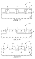
- FIG. 28 depicts alternate processing to that of FIG. 25 with respect to a substrate fragment 10 c .
- Like numerals from the above-described embodiments have been utilized where appropriate, with construction differences being indicated with the suffix “c” or with different numerals. While the suffix “c” indicates different construction, example material for such constructions is the same as used in the above embodiments for the same numerals without the suffix “c”.
- FIGS. 18-24 Prior to the processing of FIGS. 18-24 has occurred wherein material 40 b of FIG.
- first alterable material 18 may be considered as a first alterable material which was formed over spaced first features 14 , and which was altered with material from spaced first features 14 to form a first altered material 44 b on sidewalls of spaced first features 14 .
- First material 20 b was deposited over first altered material 44 b . Only a portion of first material 20 b was subsequently removed to expose first altered material 44 b and form spaced material 20 b .
- First altered material was etched from between spaced first material 20 b and spaced first features 14 . Width of spaced first material 20 b was laterally trimmed, and spaced second features 22 b have been formed. Alternately, unaltered of the alterable material may be used in place of the first material, as described above.
- a second alterable material 60 has been deposited over spaced first features 14 and over the spaced first material 20 b .
- Composition and attributes of second alterable material 60 are the same as that described above for alterable material 40 and depending at least in part on composition of spaced first features 14 and spaced second features 22 b.
- second alterable material 60 has been altered with material from spaced first features 14 and with material from spaced first material/spaced second features 22 c to form second altered material 62 on sidewalls of spaced first features 14 and on sidewalls of spaced first material/spaced second features 22 c.
- unaltered second alterable material 60 (not shown) has been removed from the substrate selectively relative to second altered material 62 .
- second altered material 62 has been anisotropically etched to form spacers 30 c.
- first features 14 (not shown) and first material/spaced second features 22 b (not shown) have been removed from the substrate, thereby forming a mask pattern 49 comprising second altered material 62 .
- Substrate 12 would be processed through mask pattern 49 , for example using any technique as described above.
Landscapes
- Engineering & Computer Science (AREA)
- Physics & Mathematics (AREA)
- General Physics & Mathematics (AREA)
- Computer Hardware Design (AREA)
- Power Engineering (AREA)
- Condensed Matter Physics & Semiconductors (AREA)
- Microelectronics & Electronic Packaging (AREA)
- Manufacturing & Machinery (AREA)
- Chemical & Material Sciences (AREA)
- Inorganic Chemistry (AREA)
- Chemical Kinetics & Catalysis (AREA)
- General Chemical & Material Sciences (AREA)
- Drying Of Semiconductors (AREA)
- Internal Circuitry In Semiconductor Integrated Circuit Devices (AREA)
- Semiconductor Memories (AREA)
- Manufacturing Of Printed Wiring (AREA)
- Micromachines (AREA)
- Exposure Of Semiconductors, Excluding Electron Or Ion Beam Exposure (AREA)
Abstract
Description
Claims (37)
Priority Applications (1)
| Application Number | Priority Date | Filing Date | Title |
|---|---|---|---|
| US13/561,424 US8703570B2 (en) | 2008-12-04 | 2012-07-30 | Methods of fabricating substrates |
Applications Claiming Priority (2)
| Application Number | Priority Date | Filing Date | Title |
|---|---|---|---|
| US12/328,464 US8247302B2 (en) | 2008-12-04 | 2008-12-04 | Methods of fabricating substrates |
| US13/561,424 US8703570B2 (en) | 2008-12-04 | 2012-07-30 | Methods of fabricating substrates |
Related Parent Applications (1)
| Application Number | Title | Priority Date | Filing Date |
|---|---|---|---|
| US12/328,464 Continuation US8247302B2 (en) | 2008-12-04 | 2008-12-04 | Methods of fabricating substrates |
Publications (2)
| Publication Number | Publication Date |
|---|---|
| US20120295445A1 US20120295445A1 (en) | 2012-11-22 |
| US8703570B2 true US8703570B2 (en) | 2014-04-22 |
Family
ID=42231569
Family Applications (2)
| Application Number | Title | Priority Date | Filing Date |
|---|---|---|---|
| US12/328,464 Active 2030-11-23 US8247302B2 (en) | 2008-12-04 | 2008-12-04 | Methods of fabricating substrates |
| US13/561,424 Active US8703570B2 (en) | 2008-12-04 | 2012-07-30 | Methods of fabricating substrates |
Family Applications Before (1)
| Application Number | Title | Priority Date | Filing Date |
|---|---|---|---|
| US12/328,464 Active 2030-11-23 US8247302B2 (en) | 2008-12-04 | 2008-12-04 | Methods of fabricating substrates |
Country Status (8)
| Country | Link |
|---|---|
| US (2) | US8247302B2 (en) |
| EP (1) | EP2353173B1 (en) |
| JP (1) | JP5418923B2 (en) |
| KR (1) | KR101428845B1 (en) |
| CN (1) | CN102239539B (en) |
| SG (1) | SG171865A1 (en) |
| TW (1) | TWI405244B (en) |
| WO (1) | WO2010065249A2 (en) |
Cited By (1)
| Publication number | Priority date | Publication date | Assignee | Title |
|---|---|---|---|---|
| US9457450B2 (en) | 2013-03-08 | 2016-10-04 | Tera Xtal Technology Corporation | Pad conditioning tool |
Families Citing this family (34)
| Publication number | Priority date | Publication date | Assignee | Title |
|---|---|---|---|---|
| US8852851B2 (en) | 2006-07-10 | 2014-10-07 | Micron Technology, Inc. | Pitch reduction technology using alternating spacer depositions during the formation of a semiconductor device and systems including same |
| US7790360B2 (en) * | 2007-03-05 | 2010-09-07 | Micron Technology, Inc. | Methods of forming multiple lines |
| US7989307B2 (en) | 2008-05-05 | 2011-08-02 | Micron Technology, Inc. | Methods of forming isolated active areas, trenches, and conductive lines in semiconductor structures and semiconductor structures including the same |
| US10151981B2 (en) | 2008-05-22 | 2018-12-11 | Micron Technology, Inc. | Methods of forming structures supported by semiconductor substrates |
| US8796155B2 (en) | 2008-12-04 | 2014-08-05 | Micron Technology, Inc. | Methods of fabricating substrates |
| US8247302B2 (en) | 2008-12-04 | 2012-08-21 | Micron Technology, Inc. | Methods of fabricating substrates |
| US8273634B2 (en) * | 2008-12-04 | 2012-09-25 | Micron Technology, Inc. | Methods of fabricating substrates |
| US8692310B2 (en) | 2009-02-09 | 2014-04-08 | Spansion Llc | Gate fringing effect based channel formation for semiconductor device |
| NL2004276A (en) * | 2009-03-04 | 2010-09-06 | Asml Netherlands Bv | A method of measuring a characteristic. |
| US8268543B2 (en) * | 2009-03-23 | 2012-09-18 | Micron Technology, Inc. | Methods of forming patterns on substrates |
| US9330934B2 (en) | 2009-05-18 | 2016-05-03 | Micron Technology, Inc. | Methods of forming patterns on substrates |
| US20110129991A1 (en) * | 2009-12-02 | 2011-06-02 | Kyle Armstrong | Methods Of Patterning Materials, And Methods Of Forming Memory Cells |
| US8518788B2 (en) | 2010-08-11 | 2013-08-27 | Micron Technology, Inc. | Methods of forming a plurality of capacitors |
| US8455341B2 (en) | 2010-09-02 | 2013-06-04 | Micron Technology, Inc. | Methods of forming features of integrated circuitry |
| US8575032B2 (en) | 2011-05-05 | 2013-11-05 | Micron Technology, Inc. | Methods of forming a pattern on a substrate |
| KR101807665B1 (en) | 2011-08-23 | 2017-12-12 | 삼성전자 주식회사 | Method of forming micropatterns |
| US9076680B2 (en) | 2011-10-18 | 2015-07-07 | Micron Technology, Inc. | Integrated circuitry, methods of forming capacitors, and methods of forming integrated circuitry comprising an array of capacitors and circuitry peripheral to the array |
| US9177794B2 (en) | 2012-01-13 | 2015-11-03 | Micron Technology, Inc. | Methods of patterning substrates |
| US8629048B1 (en) | 2012-07-06 | 2014-01-14 | Micron Technology, Inc. | Methods of forming a pattern on a substrate |
| US20140054756A1 (en) * | 2012-08-23 | 2014-02-27 | Michael Hyatt | Anti spacer process and semiconductor structure generated by the anti spacer process |
| WO2014122709A1 (en) | 2013-02-07 | 2014-08-14 | シャープ株式会社 | Semiconductor device and method for manufacturing same |
| US8932957B2 (en) * | 2013-03-12 | 2015-01-13 | Taiwan Semiconductor Manufacturing Company, Ltd. | Method of fabricating a FinFET device |
| US9153478B2 (en) | 2013-03-15 | 2015-10-06 | Taiwan Semiconductor Manufacturing Company, Ltd. | Spacer etching process for integrated circuit design |
| KR102104058B1 (en) | 2013-09-27 | 2020-04-23 | 삼성전자 주식회사 | Semiconductor device and method of manufacturing the same |
| US9177797B2 (en) * | 2013-12-04 | 2015-11-03 | Taiwan Semiconductor Manufacturing Company, Ltd. | Lithography using high selectivity spacers for pitch reduction |
| CN103996602B (en) * | 2014-06-09 | 2016-08-31 | 上海华力微电子有限公司 | A kind of method using bilateral wall technique to form ultralow size figure |
| TWI632437B (en) * | 2014-11-07 | 2018-08-11 | 羅門哈斯電子材料有限公司 | Methods of forming relief images |
| US9786503B2 (en) * | 2015-04-08 | 2017-10-10 | Tokyo Electron Limited | Method for increasing pattern density in self-aligned patterning schemes without using hard masks |
| US9455177B1 (en) * | 2015-08-31 | 2016-09-27 | Dow Global Technologies Llc | Contact hole formation methods |
| KR102447178B1 (en) * | 2015-09-01 | 2022-09-26 | 삼성전자주식회사 | Methods of manufacturing semiconductor devices |
| US9882028B2 (en) * | 2016-06-29 | 2018-01-30 | International Business Machines Corporation | Pitch split patterning for semiconductor devices |
| US10217633B2 (en) * | 2017-03-13 | 2019-02-26 | Globalfoundries Inc. | Substantially defect-free polysilicon gate arrays |
| US10475648B1 (en) * | 2018-05-01 | 2019-11-12 | United Microelectronics Corp. | Method for patterning a semiconductor structure |
| DE102019118612B4 (en) * | 2018-09-28 | 2024-02-08 | Taiwan Semiconductor Manufacturing Co., Ltd. | LITHOGRAPHY PROCESS FOR SEMICONDUCTOR PACKAGING AND RESULTING STRUCTURES |
Citations (217)
| Publication number | Priority date | Publication date | Assignee | Title |
|---|---|---|---|---|
| EP0171111A3 (en) | 1984-07-13 | 1987-07-22 | BELL TELEPHONE MANUFACTURING COMPANY Naamloze Vennootschap | Process to superpose two positive photoresist layers |
| US4910168A (en) * | 1988-05-06 | 1990-03-20 | Mos Electronics Corporation | Method to reduce silicon area for via formation |
| US5008207A (en) * | 1989-09-11 | 1991-04-16 | International Business Machines Corporation | Method of fabricating a narrow base transistor |
| US5013680A (en) | 1990-07-18 | 1991-05-07 | Micron Technology, Inc. | Process for fabricating a DRAM array having feature widths that transcend the resolution limit of available photolithography |
| US5047117A (en) | 1990-09-26 | 1991-09-10 | Micron Technology, Inc. | Method of forming a narrow self-aligned, annular opening in a masking layer |
| US5254218A (en) | 1992-04-22 | 1993-10-19 | Micron Technology, Inc. | Masking layer having narrow isolated spacings and the method for forming said masking layer and the method for forming narrow isolated trenches defined by said masking layer |
| US5328810A (en) | 1990-05-07 | 1994-07-12 | Micron Technology, Inc. | Method for reducing, by a factor or 2-N, the minimum masking pitch of a photolithographic process |
| US5372916A (en) | 1991-09-12 | 1994-12-13 | Hitachi, Ltd. | X-ray exposure method with an X-ray mask comprising phase shifter sidewalls |
| US5382315A (en) | 1991-02-11 | 1995-01-17 | Microelectronics And Computer Technology Corporation | Method of forming etch mask using particle beam deposition |
| US5420067A (en) | 1990-09-28 | 1995-05-30 | The United States Of America As Represented By The Secretary Of The Navy | Method of fabricatring sub-half-micron trenches and holes |
| US5429988A (en) | 1994-06-13 | 1995-07-04 | United Microelectronics Corporation | Process for producing high density conductive lines |
| US5573837A (en) | 1992-04-22 | 1996-11-12 | Micron Technology, Inc. | Masking layer having narrow isolated spacings and the method for forming said masking layer and the method for forming narrow isolated trenches defined by said masking layer |
| US5593813A (en) | 1994-07-14 | 1997-01-14 | Hyundai Electronics Industries Co. Ltd. | Method for forming submicroscopic patterns |
| US5616510A (en) | 1992-11-02 | 1997-04-01 | Wong; Chun C. D. | Method for making multimedia storage system with highly compact memory cells |
| US5905279A (en) | 1996-04-09 | 1999-05-18 | Kabushiki Kaisha Toshiba | Low resistant trench fill for a semiconductor device |
| US5916821A (en) | 1995-07-17 | 1999-06-29 | Siemens Aktiengesellschaft | Method for producing sublithographic etching masks |
| US6063688A (en) | 1997-09-29 | 2000-05-16 | Intel Corporation | Fabrication of deep submicron structures and quantum wire transistors using hard-mask transistor width definition |
| US6087263A (en) | 1998-01-29 | 2000-07-11 | Micron Technology, Inc. | Methods of forming integrated circuitry and integrated circuitry structures |
| US6140217A (en) | 1998-07-16 | 2000-10-31 | International Business Machines Corporation | Technique for extending the limits of photolithography |
| US6207490B1 (en) | 1997-12-11 | 2001-03-27 | Samsung Electronics Co., Ltd. | Semiconductor device and method for fabricating the same |
| US6235574B1 (en) | 1999-03-22 | 2001-05-22 | Infineon North America Corp. | High performance DRAM and method of manufacture |
| US6249335B1 (en) | 1992-01-17 | 2001-06-19 | Nikon Corporation | Photo-mask and method of exposing and projection-exposing apparatus |
| US6303272B1 (en) | 1998-11-13 | 2001-10-16 | International Business Machines Corporation | Process for self-alignment of sub-critical contacts to wiring |
| US20020037617A1 (en) | 2000-06-29 | 2002-03-28 | Kim Jun Dong | Method for forming gate electrodes in a semicoductor device using formed fine patterns |
| JP3270227B2 (en) | 1993-05-26 | 2002-04-02 | 富士写真フイルム株式会社 | Electric hoist |
| US6383952B1 (en) | 2001-02-28 | 2002-05-07 | Advanced Micro Devices, Inc. | RELACS process to double the frequency or pitch of small feature formation |
| US20020094688A1 (en) | 2001-01-16 | 2002-07-18 | Semiconductor Leading Edge Technologies, Inc. | Method of forming fine patterns |
| US6429123B1 (en) | 2000-10-04 | 2002-08-06 | Vanguard International Semiconductor Corporation | Method of manufacturing buried metal lines having ultra fine features |
| US20020130348A1 (en) | 2001-03-16 | 2002-09-19 | Tran Luan C. | 6F2 dram array, a dram array formed on a semiconductive substrate, a method of forming memory cells in a 6F2 dram array and a method of isolating a single row of memory cells in a 6F2 dram array |
| US20030001214A1 (en) | 1997-06-20 | 2003-01-02 | Makoto Yoshida | Semiconductor integrated circuit device and manufacturing method thereof |
| EP1273974A2 (en) | 2001-07-05 | 2003-01-08 | Tokyo Ohka Kogyo Co., Ltd. | Method for reducing a pattern dimension in a photoresist layer |
| US20030006410A1 (en) | 2000-03-01 | 2003-01-09 | Brian Doyle | Quantum wire gate device and method of making same |
| US6548385B1 (en) | 2002-06-12 | 2003-04-15 | Jiun-Ren Lai | Method for reducing pitch between conductive features, and structure formed using the method |
| US6548401B1 (en) | 2002-01-23 | 2003-04-15 | Micron Technology, Inc. | Semiconductor processing methods, and semiconductor constructions |
| US20030091936A1 (en) | 2001-08-31 | 2003-05-15 | Jorg Rottstegge | Process for sidewall amplification of resist structures and for the production of structures having reduced structure size |
| US6566280B1 (en) | 2002-08-26 | 2003-05-20 | Intel Corporation | Forming polymer features on a substrate |
| US6580136B2 (en) | 2001-01-30 | 2003-06-17 | International Business Machines Corporation | Method for delineation of eDRAM support device notched gate |
| KR20030049198A (en) | 2001-12-14 | 2003-06-25 | 주식회사 하이닉스반도체 | Forming method of photoresist pattern improving etching resistance by relacs material |
| KR20030056601A (en) | 2001-12-28 | 2003-07-04 | 주식회사 하이닉스반도체 | Method of forming a source line in flash memory device |
| US6599844B2 (en) | 2000-06-22 | 2003-07-29 | Hyundai Electronics Industries, Co., Ltd. | Method and forming fine patterns of semiconductor devices using passivation layers |
| US6605541B1 (en) | 1998-05-07 | 2003-08-12 | Advanced Micro Devices, Inc. | Pitch reduction using a set of offset masks |
| JP2003234279A (en) | 2002-02-08 | 2003-08-22 | Sony Corp | Forming method of resist pattern, manufacturing method of semiconductor device and forming device for resist pattern |
| US6627524B2 (en) | 2001-06-06 | 2003-09-30 | Micron Technology, Inc. | Methods of forming transistor gates; and methods of forming programmable read-only memory constructions |
| US6630379B2 (en) | 2000-06-23 | 2003-10-07 | International Business Machines Corporation | Method of manufacturing 6F2 trench capacitor DRAM cell having vertical MOSFET and 3F bitline pitch |
| US6638441B2 (en) | 2002-01-07 | 2003-10-28 | Macronix International Co., Ltd. | Method for pitch reduction |
| KR20030089063A (en) | 2002-05-16 | 2003-11-21 | 주식회사 하이닉스반도체 | Forming method of photoresist pattern |
| US6667502B1 (en) | 1999-08-31 | 2003-12-23 | Micron Technology, Inc. | Structurally-stabilized capacitors and method of making of same |
| US6703323B2 (en) | 2001-12-14 | 2004-03-09 | Hynix Semiconductor Inc | Method of inhibiting pattern collapse using a relacs material |
| US6710390B2 (en) | 1997-07-03 | 2004-03-23 | Micron Technology, Inc. | Capacitors and DRAM arrays |
| JP2004134574A (en) | 2002-10-10 | 2004-04-30 | Renesas Technology Corp | Manufacturing method of semiconductor device |
| US6734107B2 (en) | 2002-06-12 | 2004-05-11 | Macronix International Co., Ltd. | Pitch reduction in semiconductor fabrication |
| US6735132B2 (en) | 2001-07-23 | 2004-05-11 | Micron Technology, Inc. | 6F2 DRAM array with apparatus for stress testing an isolation gate and method |
| US6753220B2 (en) | 1996-11-01 | 2004-06-22 | Micron Technology, Inc. | Semiconductor processing methods of forming devices on a substrate, forming device arrays on a substrate, forming conductive lines on a substrate, and forming capacitor arrays on a substrate, and integrated circuitry |
| US6756619B2 (en) | 2002-08-26 | 2004-06-29 | Micron Technology, Inc. | Semiconductor constructions |
| KR20040057582A (en) | 2002-12-26 | 2004-07-02 | 주식회사 하이닉스반도체 | Method of forming a micro pattern having a dual damascene |
| US6774051B2 (en) | 2002-06-12 | 2004-08-10 | Macronix International Co., Ltd. | Method for reducing pitch |
| JP2004247399A (en) | 2003-02-12 | 2004-09-02 | Renesas Technology Corp | Method for manufacturing semiconductor device |
| US20040198065A1 (en) | 2003-04-04 | 2004-10-07 | Sung-Kwon Lee | Method for fabricating semiconductor device with fine patterns |
| US6826069B2 (en) | 2001-03-14 | 2004-11-30 | Atmos Corporation | Interleaved wordline architecture |
| US20040253535A1 (en) | 2002-11-20 | 2004-12-16 | Shipley Company, L.L.C. | Multilayer photoresist systems |
| US6864184B1 (en) | 2004-02-05 | 2005-03-08 | Advanced Micro Devices, Inc. | Method for reducing critical dimension attainable via the use of an organic conforming layer |
| US6872512B2 (en) | 2002-03-27 | 2005-03-29 | Nec Lcd Technologies, Ltd. | Method of forming resist pattern |
| US6905975B2 (en) | 2003-07-03 | 2005-06-14 | Micron Technology, Inc. | Methods of forming patterned compositions |
| US20050130068A1 (en) | 2003-11-21 | 2005-06-16 | Takehiro Kondoh | Pattern forming method and method for manufacturing a semiconductor device |
| US20050142497A1 (en) | 2003-12-26 | 2005-06-30 | Samsung Electronics Co., Ltd. | Method of forming a pattern in a semiconductor device and method of forming a gate using the same |
| US6916594B2 (en) | 2002-12-30 | 2005-07-12 | Hynix Semiconductor Inc. | Overcoating composition for photoresist and method for forming photoresist pattern using the same |
| US20050164478A1 (en) | 2004-01-26 | 2005-07-28 | Taiwan Semiconductor Manufacturing Co. | Novel method of trimming technology |
| US20050173740A1 (en) | 2004-02-07 | 2005-08-11 | You-Seung Jin | Multi-gate transistor formed with active patterns of uniform critical dimension |
| JP2005243681A (en) | 2004-02-24 | 2005-09-08 | Tokyo Electron Ltd | Film modifying method, film modifying apparatus and control method of amount of slimming |
| US6951822B2 (en) | 2001-09-28 | 2005-10-04 | Infineon Technologies North America Corp. | Method for forming inside nitride spacer for deep trench device DRAM cell |
| US20050255696A1 (en) | 2003-05-09 | 2005-11-17 | Fujitsu Limited | Method of processing resist, semiconductor device, and method of producing the same |
| US20050272220A1 (en) | 2004-06-07 | 2005-12-08 | Carlo Waldfried | Ultraviolet curing process for spin-on dielectric materials used in pre-metal and/or shallow trench isolation applications |
| US20060011947A1 (en) | 2004-05-26 | 2006-01-19 | Werner Juengling | Semiconductor structures and memory device constructions |
| US20060024621A1 (en) | 2004-07-17 | 2006-02-02 | Infineon Technologies Ag | Method of producing a structure on the surface of a substrate |
| US20060046484A1 (en) | 2004-09-02 | 2006-03-02 | Abatchev Mirzafer K | Method for integrated circuit fabrication using pitch multiplication |
| US20060046200A1 (en) | 2004-09-01 | 2006-03-02 | Abatchev Mirzafer K | Mask material conversion |
| US20060046422A1 (en) | 2004-08-31 | 2006-03-02 | Micron Technology, Inc. | Methods for increasing photo alignment margins |
| US20060063384A1 (en) | 2004-09-23 | 2006-03-23 | Jung-Hwan Hah | Mask patterns for semiconductor device fabrication and related methods and structures |
| US7023069B2 (en) | 2003-12-19 | 2006-04-04 | Third Dimension (3D) Semiconductor, Inc. | Method for forming thick dielectric regions using etched trenches |
| CN1761063A (en) | 2004-10-14 | 2006-04-19 | 茂德科技股份有限公司 | Structure of dynamic RAM |
| US20060088788A1 (en) | 2004-10-26 | 2006-04-27 | Takanori Kudo | Composition for coating over a photoresist pattern |
| US7037840B2 (en) | 2004-01-26 | 2006-05-02 | Micron Technology, Inc. | Methods of forming planarized surfaces over semiconductor substrates |
| US7049652B2 (en) | 2003-12-10 | 2006-05-23 | Sandisk Corporation | Pillar cell flash memory technology |
| US20060115978A1 (en) | 2004-11-30 | 2006-06-01 | Michael Specht | Charge-trapping memory cell and method for production |
| US20060118785A1 (en) | 2003-09-12 | 2006-06-08 | International Business Machines Corporation | Techniques for patterning features in semiconductor devices |
| US7064376B2 (en) | 1996-05-24 | 2006-06-20 | Jeng-Jye Shau | High performance embedded semiconductor memory devices with multiple dimension first-level bit-lines |
| US7067385B2 (en) | 2003-09-04 | 2006-06-27 | Micron Technology, Inc. | Support for vertically oriented capacitors during the formation of a semiconductor device |
| US7074533B2 (en) | 2003-05-05 | 2006-07-11 | Xerox Corporation | Photoconductive members |
| US20060154182A1 (en) | 2005-01-12 | 2006-07-13 | International Business Machines Corporation | Method for post lithographic critical dimension shrinking using post overcoat planarization |
| US7125781B2 (en) | 2003-09-04 | 2006-10-24 | Micron Technology, Inc. | Methods of forming capacitor devices |
| US20060240361A1 (en) | 2005-04-21 | 2006-10-26 | Ji-Young Lee | Method of forming small pitch pattern using double spacers |
| US20060263699A1 (en) | 2005-05-23 | 2006-11-23 | Mirzafer Abatchev | Methods for forming arrays of a small, closely spaced features |
| US20060273456A1 (en) | 2005-06-02 | 2006-12-07 | Micron Technology, Inc., A Corporation | Multiple spacer steps for pitch multiplication |
| US20060281266A1 (en) | 2005-06-09 | 2006-12-14 | Wells David H | Method and apparatus for adjusting feature size and position |
| US20060278911A1 (en) | 2005-06-14 | 2006-12-14 | Eppich Anton P | Relaxed-pitch method of aligning active area to digit line |
| US20060286795A1 (en) | 2005-06-21 | 2006-12-21 | Kabushiki Kaisha Toshiba | Method of manufacturing semiconductor device |
| US20070003878A1 (en) | 2005-03-23 | 2007-01-04 | Asml Netherlands B.V. | Reduced pitch multiple exposure process |
| US20070010058A1 (en) | 2005-07-08 | 2007-01-11 | Micron Technology, Inc. | Method and apparatus for a self-aligned recessed access device (RAD) transistor gate |
| TW200702903A (en) | 2005-06-28 | 2007-01-16 | Lam Res Corp | Multiple mask process with etch mask stack |
| US7166533B2 (en) | 2005-04-08 | 2007-01-23 | Infineon Technologies, Ag | Phase change memory cell defined by a pattern shrink material process |
| US20070020565A1 (en) | 2005-07-25 | 2007-01-25 | Samsung Electronics Co., Ltd. | Methods of fabricating a semiconductor device |
| JP2007017993A (en) | 2006-08-22 | 2007-01-25 | Fujitsu Ltd | Resist pattern, method for manufacturing the same, and semiconductor device and method for manufacturing the same |
| US20070026684A1 (en) | 2005-08-01 | 2007-02-01 | Stefano Parascandola | Method of producing pitch fractionizations in semiconductor technology |
| US20070023805A1 (en) | 2005-07-26 | 2007-02-01 | Wells David H | Reverse construction memory cell |
| US20070037066A1 (en) | 2005-08-09 | 2007-02-15 | Li-Tung Hsiao | Method for correcting and configuring optical mask pattern |
| US20070048930A1 (en) | 2005-09-01 | 2007-03-01 | Figura Thomas A | Peripheral gate stacks and recessed array gates |
| US20070049011A1 (en) | 2005-09-01 | 2007-03-01 | Micron Technology, Inc., A Corporation | Method of forming isolated features using pitch multiplication |
| US20070049003A1 (en) | 2005-09-01 | 2007-03-01 | John Smythe | Semiconductor constructions and methods of forming layers |
| US20070049035A1 (en) | 2005-08-31 | 2007-03-01 | Tran Luan C | Method of forming pitch multipled contacts |
| US20070049040A1 (en) | 2005-03-15 | 2007-03-01 | Micron Technology, Inc., A Corporation | Multiple deposition for integration of spacers in pitch multiplication process |
| US20070048674A1 (en) | 2005-09-01 | 2007-03-01 | Wells David H | Methods for forming arrays of small, closely spaced features |
| US20070045712A1 (en) | 2005-09-01 | 2007-03-01 | Haller Gordon A | Memory cell layout and process flow |
| US20070049030A1 (en) | 2005-09-01 | 2007-03-01 | Sandhu Gurtej S | Pitch multiplication spacers and methods of forming the same |
| US7199005B2 (en) | 2005-08-02 | 2007-04-03 | Micron Technology, Inc. | Methods of forming pluralities of capacitors |
| US20070077743A1 (en) | 2005-09-30 | 2007-04-05 | Rao Rajesh A | Multiple fin formation |
| US20070077524A1 (en) | 2005-09-30 | 2007-04-05 | Samsung Electronics Co., Ltd. | Method for forming patterns of semiconductor device |
| US7202174B1 (en) | 2006-02-02 | 2007-04-10 | Hynix Semiconductor Inc. | Method of forming micro pattern in semiconductor device |
| US7202127B2 (en) | 2004-08-27 | 2007-04-10 | Micron Technology, Inc. | Methods of forming a plurality of capacitors |
| US20070085152A1 (en) | 2005-10-14 | 2007-04-19 | Promos Technologies Pte.Ltd. Singapore | Reduced area dynamic random access memory (DRAM) cell and method for fabricating the same |
| US20070096182A1 (en) | 2004-09-10 | 2007-05-03 | Infineon Technologies Ag | Transistor, meomory cell array and method of manufacturing a transistor |
| US20070099431A1 (en) | 2005-11-01 | 2007-05-03 | Micron Technology, Inc. | Process for increasing feature density during the manufacture of a semiconductor device |
| US20070105357A1 (en) | 2005-09-01 | 2007-05-10 | Micron Technology, Inc. | Silicided recessed silicon |
| US20070123015A1 (en) | 2005-11-30 | 2007-05-31 | International Business Machines Corporation | Passive components in the back end of integrated circuits |
| US7230292B2 (en) | 2003-08-05 | 2007-06-12 | Micron Technology, Inc. | Stud electrode and process for making same |
| US20070145464A1 (en) | 2002-08-29 | 2007-06-28 | Voshell Thomas W | Random access memory device utilizing a vertically oriented select transistor |
| US20070161251A1 (en) | 2005-03-15 | 2007-07-12 | Micron Technology, Inc. | Pitch reduced patterns relative to photolithography features |
| US20070181929A1 (en) | 2005-06-27 | 2007-08-09 | Micron Technology, Inc. | Semiconductor Constructions, Memory Cells, DRAM Arrays, Electronic Systems; Methods of Forming Semiconductor Constructions; and Methods of Forming DRAM Arrays |
| US20070190463A1 (en) | 2004-09-02 | 2007-08-16 | Micron Technology, Inc. | Method to align mask patterns |
| US20070197014A1 (en) | 2006-02-17 | 2007-08-23 | Samsung Electronics Co., Ltd. | Method of fabricating semiconductor device |
| CN101026087A (en) | 2006-02-24 | 2007-08-29 | 海力士半导体有限公司 | Method for forming fine pattern of semiconductor device |
| US20070202697A1 (en) | 2006-02-24 | 2007-08-30 | Hynix Semiconductor Inc. | Method for forming fine pattern of semiconductor device |
| US20070205438A1 (en) | 2006-03-02 | 2007-09-06 | Werner Juengling | Masking process for simultaneously patterning separate regions |
| US20070205443A1 (en) | 2006-03-02 | 2007-09-06 | Werner Juengling | Vertical gated access transistor |
| US20070224537A1 (en) | 2006-03-24 | 2007-09-27 | Fujitsu Limited | Resist composition, method for forming resist pattern, and semiconductor device and method for manufacturing the same |
| US20070238299A1 (en) | 2006-04-07 | 2007-10-11 | Micron Technology, Inc. | Simplified pitch doubling process flow |
| US20070238053A1 (en) | 2006-04-11 | 2007-10-11 | Koji Hashimoto | Manufacturing method of semiconductor device |
| US20070248916A1 (en) | 2006-04-21 | 2007-10-25 | Tdk Corporation | Resist pattern forming method, thin-film pattern forming method, and microdevice manufacturing method |
| US20070261016A1 (en) | 2006-04-24 | 2007-11-08 | Sandhu Gurtej S | Masking techniques and templates for dense semiconductor fabrication |
| US20070264830A1 (en) | 2006-05-10 | 2007-11-15 | Lam Research Corporation | Pitch reduction |
| US20070264828A1 (en) | 2006-05-09 | 2007-11-15 | Hynix Semiconductor Inc. | Method for forming fine pattern of semiconductor device |
| US20070281219A1 (en) | 2006-06-01 | 2007-12-06 | Sandhu Gurtej S | Masking techniques and contact imprint reticles for dense semiconductor fabrication |
| US20070278183A1 (en) | 2006-06-02 | 2007-12-06 | Whonchee Lee | Wet etch suitable for creating square cuts in si and resulting structures |
| KR100784062B1 (en) | 2006-01-20 | 2007-12-10 | 주식회사 하이닉스반도체 | Method for forming micro pattern in semiconductor device |
| US20080008969A1 (en) | 2006-07-10 | 2008-01-10 | Micron Technology, Inc. | Pitch reduction technology using alternating spacer depositions during the formation of a semiconductor device and systems including same |
| US7320911B2 (en) | 2004-12-06 | 2008-01-22 | Micron Technology, Inc. | Methods of forming pluralities of capacitors |
| US20080026327A1 (en) | 2006-07-14 | 2008-01-31 | Hynix Semiconductor Inc. | Method for forming fine pattern with a double exposure technology |
| US20080032243A1 (en) | 2005-05-30 | 2008-02-07 | Hynix Semiconductor Inc. | Photoresist Coating Composition and Method for Forming Fine Contact of Semiconductor Device |
| US20080032508A1 (en) | 2006-08-07 | 2008-02-07 | Taiwan Semiconductor Manufacturing Company, Ltd. | Method and Material For Forming A Double Exposure Lithography Pattern |
| US20080044770A1 (en) | 2006-08-17 | 2008-02-21 | Fujitsu Limited | Process for forming resist pattern, semiconductor device and manufacturing method for the same |
| US20080057692A1 (en) | 2006-08-30 | 2008-03-06 | Wells David H | Single spacer process for multiplying pitch by a factor greater than two and related intermediate IC structures |
| US20080064213A1 (en) | 2006-09-12 | 2008-03-13 | Hynix Semiconductor Inc. | Method for forming a fine pattern of a semiconductor device |
| US20080063986A1 (en) | 2006-09-12 | 2008-03-13 | Hynix Semiconductor Inc. | Method of forming fine pattern of semiconductor device |
| US20080070165A1 (en) | 2006-09-14 | 2008-03-20 | Mark Fischer | Efficient pitch multiplication process |
| US20080076070A1 (en) | 2006-09-08 | 2008-03-27 | Samsung Electronics Co., Ltd. | Methods of Forming Fine Patterns In Integrated Circuits Using Atomic Layer Deposition |
| US20080085612A1 (en) | 2006-10-05 | 2008-04-10 | Micron Technology, Inc. | Method to deposit conformal low temperature SiO2 |
| US20080090416A1 (en) | 2006-10-11 | 2008-04-17 | Micro Technology, Inc. | Methods of etching polysilicon and methods of forming pluralities of capacitors |
| KR20080038963A (en) | 2006-10-31 | 2008-05-07 | 주식회사 하이닉스반도체 | Method for mamufacturing semicondutor device with contact |
| US20080113483A1 (en) | 2006-11-15 | 2008-05-15 | Micron Technology, Inc. | Methods of etching a pattern layer to form staggered heights therein and intermediate semiconductor device structures |
| US20080113511A1 (en) | 2006-11-10 | 2008-05-15 | Sang-Joon Park | Method of forming fine patterns using double patterning process |
| US20080122125A1 (en) | 2006-11-29 | 2008-05-29 | Micron Technology, Inc. | Methods to reduce the critical dimension of semiconductor devices and partially fabricated semiconductor devices having reduced critical dimensions |
| US20080120900A1 (en) | 2006-11-29 | 2008-05-29 | Femo Operations, Lp | Systems and Methods for Repelling and/or Killing Pests Using Mulch |
| US7384849B2 (en) | 2005-03-25 | 2008-06-10 | Micron Technology, Inc. | Methods of forming recessed access devices associated with semiconductor constructions |
| US7387939B2 (en) | 2004-07-19 | 2008-06-17 | Micron Technology, Inc. | Methods of forming semiconductor structures and capacitor devices |
| US7390750B1 (en) | 2004-03-23 | 2008-06-24 | Cypress Semiconductor Corp. | Method of patterning elements within a semiconductor topography |
| US7390749B2 (en) | 2005-11-30 | 2008-06-24 | Lam Research Corporation | Self-aligned pitch reduction |
| US20080171438A1 (en) | 2007-01-11 | 2008-07-17 | Micron Technology, Inc. | Methods of uniformly removing silicon oxide, a method of removing a sacrifical oxide, and an intermediate semiconductor device structure |
| US20080171446A1 (en) | 2007-01-12 | 2008-07-17 | Advanced Micro Devices, Inc. | Method of forming semiconductor device |
| US20080176406A1 (en) | 2007-01-22 | 2008-07-24 | Shuji Ikeda | Methods for Fabricating Semiconductor Structures |
| US20080199814A1 (en) | 2006-12-06 | 2008-08-21 | Fujifilm Electronic Materials, U.S.A., Inc. | Device manufacturing process utilizing a double patterning process |
| US20080199806A1 (en) | 2007-02-16 | 2008-08-21 | Shin-Etsu Chemical Co., Ltd. | Patterning process and resist composition |
| US20080206950A1 (en) | 2007-02-26 | 2008-08-28 | Micron Technology, Inc. | Methods of forming a plurality of capacitors |
| US20080220600A1 (en) | 2007-03-05 | 2008-09-11 | Micron Technology, Inc. | Semiconductor constructions, methods of forming multiple lines, and methods of forming high density structures and low density structures with a single photomask |
| US7439152B2 (en) | 2004-08-27 | 2008-10-21 | Micron Technology, Inc. | Methods of forming a plurality of capacitors |
| US20080261349A1 (en) | 2005-09-01 | 2008-10-23 | Micron Technology, Inc. | Protective coating for planarization |
| US7442976B2 (en) | 2004-09-01 | 2008-10-28 | Micron Technology, Inc. | DRAM cells with vertical transistors |
| US20080292991A1 (en) | 2007-05-24 | 2008-11-27 | Advanced Micro Devices, Inc. | High fidelity multiple resist patterning |
| US20080296732A1 (en) | 2007-05-31 | 2008-12-04 | Micron Technology, Inc. | Methods of isolating array features during pitch doubling processes and semiconductor device structures having isolated array features |
| US20080305636A1 (en) | 2007-06-07 | 2008-12-11 | Samsung Electronics Co., Ltd. | Method of forming fine pattern employing self-aligned double patterning |
| US20090074958A1 (en) | 2007-09-13 | 2009-03-19 | Dequan Xiao | Polymeric nanocompositions comprising self-assembled organic quantum dots |
| US7517753B2 (en) | 2005-05-18 | 2009-04-14 | Micron Technology, Inc. | Methods of forming pluralities of capacitors |
| US7521378B2 (en) | 2004-07-01 | 2009-04-21 | Micron Technology, Inc. | Low temperature process for polysilazane oxidation/densification |
| US7521371B2 (en) | 2006-08-21 | 2009-04-21 | Micron Technology, Inc. | Methods of forming semiconductor constructions having lines |
| US7524607B2 (en) | 2003-11-17 | 2009-04-28 | Taiwan Semiconductor Manufacturing Co., Ltd. | Water soluble negative tone photoresist |
| US20090108415A1 (en) | 2007-10-31 | 2009-04-30 | Markus Lenski | Increasing etch selectivity during the patterning of a contact structure of a semiconductor device |
| US20090117739A1 (en) | 2007-11-02 | 2009-05-07 | Hynix Semiconductor Inc. | Method for forming pattern in semiconductor device |
| US20090130601A1 (en) | 2007-11-16 | 2009-05-21 | Young-Doo Jeon | Method for fabricating semiconductor device |
| US20090130852A1 (en) | 2006-04-25 | 2009-05-21 | Micron Technology, Inc. | Process for improving critical dimension uniformity of integrated circuit arrays |
| US20090130612A1 (en) | 2007-11-21 | 2009-05-21 | Macronix International Co., Ltd. | Patterning process |
| US7537866B2 (en) | 2006-05-24 | 2009-05-26 | Synopsys, Inc. | Patterning a single integrated circuit layer using multiple masks and multiple masking layers |
| US7544563B2 (en) | 2005-05-18 | 2009-06-09 | Micron Technology, Inc. | Methods of forming a plurality of capacitors |
| US7553760B2 (en) | 2006-10-19 | 2009-06-30 | International Business Machines Corporation | Sub-lithographic nano interconnect structures, and method for forming same |
| US7557013B2 (en) | 2006-04-10 | 2009-07-07 | Micron Technology, Inc. | Methods of forming a plurality of capacitors |
| US7557015B2 (en) | 2005-03-18 | 2009-07-07 | Micron Technology, Inc. | Methods of forming pluralities of capacitors |
| US20090212016A1 (en) | 2008-02-22 | 2009-08-27 | International Business Machines Corporation | Aligning polymer films |
| US20090291397A1 (en) | 2008-05-22 | 2009-11-26 | Devilliers Anton | Methods Of Forming Structures Supported By Semiconductor Substrates |
| US20090298274A1 (en) | 2008-05-29 | 2009-12-03 | Seiji Kajiwara | Method of fabricating semiconductor device |
| US20100009512A1 (en) | 2008-07-09 | 2010-01-14 | Fred Fishburn | Methods of forming a plurality of capacitors |
| US20100021573A1 (en) * | 2008-07-22 | 2010-01-28 | Michael J Gonzalez | Compositions and methods for the prevention of cardiovascular disease |
| US20100028809A1 (en) | 2006-11-14 | 2010-02-04 | Nxp, B.V. | Double patterning for lithography to increase feature spatial density |
| US20100068656A1 (en) | 2008-09-15 | 2010-03-18 | Taiwan Semiconductor Manufacturing Co., Ltd. | High etch resistant material for double patterning |
| US7682924B2 (en) | 2007-08-13 | 2010-03-23 | Micron Technology, Inc. | Methods of forming a plurality of capacitors |
| US7687387B2 (en) | 2007-08-23 | 2010-03-30 | Kabushiki Kaisha Toshiba | Semiconductor device and method of manufacturing the same |
| US20100081265A1 (en) | 2008-09-30 | 2010-04-01 | Hiromitsu Mashita | Method for manufacturing semiconductor device |
| US7696076B2 (en) | 2007-05-11 | 2010-04-13 | Hynix Semiconductor Inc. | Method of fabricating flash memory device |
| US7713818B2 (en) | 2008-04-11 | 2010-05-11 | Sandisk 3D, Llc | Double patterning method |
| US20100130015A1 (en) | 2007-06-08 | 2010-05-27 | Tokyo Electron Limited | Patterning method |
| US20100130016A1 (en) | 2008-11-24 | 2010-05-27 | Micron Technology, Inc. | Methods of forming a masking pattern for integrated circuits |
| US20100144150A1 (en) | 2008-12-04 | 2010-06-10 | Micron Technology, Inc. | Methods of Fabricating Substrates |
| US20100144151A1 (en) | 2008-12-04 | 2010-06-10 | Scott Sills | Methods of Fabricating Substrates |
| US20100144153A1 (en) | 2008-12-04 | 2010-06-10 | Scott Sills | Methods of Fabricating Substrates |
| US7851135B2 (en) | 2007-11-30 | 2010-12-14 | Hynix Semiconductor Inc. | Method of forming an etching mask pattern from developed negative and positive photoresist layers |
| US20110018055A1 (en) | 2009-07-21 | 2011-01-27 | Kabushiki Kaisha Toshiba | Power semiconductor device and method for manufacturing same |
| US20110127677A1 (en) | 2008-02-15 | 2011-06-02 | Renesas Electronics Corporation | Method of manufacturing semiconductor device, and semiconductor device |
| CN101145515B (en) | 2006-09-12 | 2011-06-29 | 海力士半导体有限公司 | Method for forming a fine pattern of a semiconductor device |
| US8083953B2 (en) | 2007-03-06 | 2011-12-27 | Micron Technology, Inc. | Registered structure formation via the application of directed thermal energy to diblock copolymer films |
| US8083958B2 (en) | 2007-12-05 | 2011-12-27 | International Business Machines Corporation | Patterning method using a combination of photolithography and copolymer self-assemblying lithography techniques |
| US8440576B2 (en) | 2008-04-25 | 2013-05-14 | Macronix International Co., Ltd. | Method for pitch reduction in integrated circuit fabrication |
Family Cites Families (12)
| Publication number | Priority date | Publication date | Assignee | Title |
|---|---|---|---|---|
| US1301485A (en) * | 1918-12-17 | 1919-04-22 | Hilmar Mueller | Pump. |
| JPS6435916A (en) * | 1987-07-31 | 1989-02-07 | Hitachi Ltd | Formation of fine pattern |
| JP3317582B2 (en) * | 1994-06-01 | 2002-08-26 | 菱電セミコンダクタシステムエンジニアリング株式会社 | Method of forming fine pattern |
| JP2006245625A (en) | 1997-06-20 | 2006-09-14 | Hitachi Ltd | Semiconductor integrated circuit device and manufacturing method therefor |
| EP1632744B1 (en) * | 2004-09-07 | 2014-08-20 | Saab Ab | A simulation system |
| JP4619839B2 (en) * | 2005-03-16 | 2011-01-26 | 株式会社東芝 | Pattern formation method |
| US7625776B2 (en) | 2006-06-02 | 2009-12-01 | Micron Technology, Inc. | Methods of fabricating intermediate semiconductor structures by selectively etching pockets of implanted silicon |
| US7709341B2 (en) | 2006-06-02 | 2010-05-04 | Micron Technology, Inc. | Methods of shaping vertical single crystal silicon walls and resulting structures |
| KR100801078B1 (en) | 2006-06-29 | 2008-02-11 | 삼성전자주식회사 | Non volatile memory integrate circuit having vertical channel and fabricating method thereof |
| KR101011490B1 (en) * | 2007-06-08 | 2011-01-31 | 도쿄엘렉트론가부시키가이샤 | Patterning method |
| KR20090001080A (en) * | 2007-06-29 | 2009-01-08 | 주식회사 하이닉스반도체 | Method of forming fine pattern of semiconductor device |
| KR20090110172A (en) * | 2008-04-17 | 2009-10-21 | 삼성전자주식회사 | Method of forming fine patterns of semiconductor device |
-
2008
- 2008-12-04 US US12/328,464 patent/US8247302B2/en active Active
-
2009
- 2009-11-11 SG SG2011039369A patent/SG171865A1/en unknown
- 2009-11-11 WO PCT/US2009/063978 patent/WO2010065249A2/en active Application Filing
- 2009-11-11 CN CN200980148546.9A patent/CN102239539B/en active Active
- 2009-11-11 KR KR1020117013503A patent/KR101428845B1/en active IP Right Grant
- 2009-11-11 JP JP2011539550A patent/JP5418923B2/en active Active
- 2009-11-11 EP EP09830818.2A patent/EP2353173B1/en active Active
- 2009-11-24 TW TW098139941A patent/TWI405244B/en active
-
2012
- 2012-07-30 US US13/561,424 patent/US8703570B2/en active Active
Patent Citations (269)
| Publication number | Priority date | Publication date | Assignee | Title |
|---|---|---|---|---|
| EP0171111A3 (en) | 1984-07-13 | 1987-07-22 | BELL TELEPHONE MANUFACTURING COMPANY Naamloze Vennootschap | Process to superpose two positive photoresist layers |
| US4910168A (en) * | 1988-05-06 | 1990-03-20 | Mos Electronics Corporation | Method to reduce silicon area for via formation |
| US5008207A (en) * | 1989-09-11 | 1991-04-16 | International Business Machines Corporation | Method of fabricating a narrow base transistor |
| US5328810A (en) | 1990-05-07 | 1994-07-12 | Micron Technology, Inc. | Method for reducing, by a factor or 2-N, the minimum masking pitch of a photolithographic process |
| US5013680A (en) | 1990-07-18 | 1991-05-07 | Micron Technology, Inc. | Process for fabricating a DRAM array having feature widths that transcend the resolution limit of available photolithography |
| US5047117A (en) | 1990-09-26 | 1991-09-10 | Micron Technology, Inc. | Method of forming a narrow self-aligned, annular opening in a masking layer |
| US5420067A (en) | 1990-09-28 | 1995-05-30 | The United States Of America As Represented By The Secretary Of The Navy | Method of fabricatring sub-half-micron trenches and holes |
| US5382315A (en) | 1991-02-11 | 1995-01-17 | Microelectronics And Computer Technology Corporation | Method of forming etch mask using particle beam deposition |
| US5372916A (en) | 1991-09-12 | 1994-12-13 | Hitachi, Ltd. | X-ray exposure method with an X-ray mask comprising phase shifter sidewalls |
| US6249335B1 (en) | 1992-01-17 | 2001-06-19 | Nikon Corporation | Photo-mask and method of exposing and projection-exposing apparatus |
| US5573837A (en) | 1992-04-22 | 1996-11-12 | Micron Technology, Inc. | Masking layer having narrow isolated spacings and the method for forming said masking layer and the method for forming narrow isolated trenches defined by said masking layer |
| US5254218A (en) | 1992-04-22 | 1993-10-19 | Micron Technology, Inc. | Masking layer having narrow isolated spacings and the method for forming said masking layer and the method for forming narrow isolated trenches defined by said masking layer |
| US5616510A (en) | 1992-11-02 | 1997-04-01 | Wong; Chun C. D. | Method for making multimedia storage system with highly compact memory cells |
| JP3270227B2 (en) | 1993-05-26 | 2002-04-02 | 富士写真フイルム株式会社 | Electric hoist |
| US5429988A (en) | 1994-06-13 | 1995-07-04 | United Microelectronics Corporation | Process for producing high density conductive lines |
| US5593813A (en) | 1994-07-14 | 1997-01-14 | Hyundai Electronics Industries Co. Ltd. | Method for forming submicroscopic patterns |
| US5916821A (en) | 1995-07-17 | 1999-06-29 | Siemens Aktiengesellschaft | Method for producing sublithographic etching masks |
| US5905279A (en) | 1996-04-09 | 1999-05-18 | Kabushiki Kaisha Toshiba | Low resistant trench fill for a semiconductor device |
| US7064376B2 (en) | 1996-05-24 | 2006-06-20 | Jeng-Jye Shau | High performance embedded semiconductor memory devices with multiple dimension first-level bit-lines |
| US6753220B2 (en) | 1996-11-01 | 2004-06-22 | Micron Technology, Inc. | Semiconductor processing methods of forming devices on a substrate, forming device arrays on a substrate, forming conductive lines on a substrate, and forming capacitor arrays on a substrate, and integrated circuitry |
| US20030001214A1 (en) | 1997-06-20 | 2003-01-02 | Makoto Yoshida | Semiconductor integrated circuit device and manufacturing method thereof |
| US6649956B2 (en) | 1997-06-20 | 2003-11-18 | Hitachi, Ltd. | Semiconductor integrated circuit device and manufacturing method thereof |
| US20040043546A1 (en) | 1997-06-20 | 2004-03-04 | Makoto Yoshida | Semiconductor integrated circuit device and manufacturing method thereof |
| US7042038B2 (en) | 1997-06-20 | 2006-05-09 | Hitachi, Ltd. | Semiconductor integrated circuit device and manufacturing method thereof |
| US6710390B2 (en) | 1997-07-03 | 2004-03-23 | Micron Technology, Inc. | Capacitors and DRAM arrays |
| US6063688A (en) | 1997-09-29 | 2000-05-16 | Intel Corporation | Fabrication of deep submicron structures and quantum wire transistors using hard-mask transistor width definition |
| US20020043690A1 (en) | 1997-09-29 | 2002-04-18 | Doyle Brian S. | Fabrication of deep submicron structures and quantum wire transistors using hard-mask transistor width definition |
| US6207490B1 (en) | 1997-12-11 | 2001-03-27 | Samsung Electronics Co., Ltd. | Semiconductor device and method for fabricating the same |
| US6087263A (en) | 1998-01-29 | 2000-07-11 | Micron Technology, Inc. | Methods of forming integrated circuitry and integrated circuitry structures |
| US6352932B1 (en) | 1998-01-29 | 2002-03-05 | Micron Technology, Inc. | Methods of forming integrated circuitry and integrated circuitry structures |
| US6605541B1 (en) | 1998-05-07 | 2003-08-12 | Advanced Micro Devices, Inc. | Pitch reduction using a set of offset masks |
| US6140217A (en) | 1998-07-16 | 2000-10-31 | International Business Machines Corporation | Technique for extending the limits of photolithography |
| US6303272B1 (en) | 1998-11-13 | 2001-10-16 | International Business Machines Corporation | Process for self-alignment of sub-critical contacts to wiring |
| US6235574B1 (en) | 1999-03-22 | 2001-05-22 | Infineon North America Corp. | High performance DRAM and method of manufacture |
| US6667502B1 (en) | 1999-08-31 | 2003-12-23 | Micron Technology, Inc. | Structurally-stabilized capacitors and method of making of same |
| US20030006410A1 (en) | 2000-03-01 | 2003-01-09 | Brian Doyle | Quantum wire gate device and method of making same |
| US6599844B2 (en) | 2000-06-22 | 2003-07-29 | Hyundai Electronics Industries, Co., Ltd. | Method and forming fine patterns of semiconductor devices using passivation layers |
| US6630379B2 (en) | 2000-06-23 | 2003-10-07 | International Business Machines Corporation | Method of manufacturing 6F2 trench capacitor DRAM cell having vertical MOSFET and 3F bitline pitch |
| US20020037617A1 (en) | 2000-06-29 | 2002-03-28 | Kim Jun Dong | Method for forming gate electrodes in a semicoductor device using formed fine patterns |
| US6429123B1 (en) | 2000-10-04 | 2002-08-06 | Vanguard International Semiconductor Corporation | Method of manufacturing buried metal lines having ultra fine features |
| JP2002217170A (en) | 2001-01-16 | 2002-08-02 | Semiconductor Leading Edge Technologies Inc | Method of forming fine pattern, method of fabricating semiconductor device and semiconductor device |
| US20020094688A1 (en) | 2001-01-16 | 2002-07-18 | Semiconductor Leading Edge Technologies, Inc. | Method of forming fine patterns |
| US6580136B2 (en) | 2001-01-30 | 2003-06-17 | International Business Machines Corporation | Method for delineation of eDRAM support device notched gate |
| US6383952B1 (en) | 2001-02-28 | 2002-05-07 | Advanced Micro Devices, Inc. | RELACS process to double the frequency or pitch of small feature formation |
| US6826069B2 (en) | 2001-03-14 | 2004-11-30 | Atmos Corporation | Interleaved wordline architecture |
| US20020130348A1 (en) | 2001-03-16 | 2002-09-19 | Tran Luan C. | 6F2 dram array, a dram array formed on a semiconductive substrate, a method of forming memory cells in a 6F2 dram array and a method of isolating a single row of memory cells in a 6F2 dram array |
| US6545904B2 (en) | 2001-03-16 | 2003-04-08 | Micron Technology, Inc. | 6f2 dram array, a dram array formed on a semiconductive substrate, a method of forming memory cells in a 6f2 dram array and a method of isolating a single row of memory cells in a 6f2 dram array |
| US6627524B2 (en) | 2001-06-06 | 2003-09-30 | Micron Technology, Inc. | Methods of forming transistor gates; and methods of forming programmable read-only memory constructions |
| US20030008968A1 (en) | 2001-07-05 | 2003-01-09 | Yoshiki Sugeta | Method for reducing pattern dimension in photoresist layer |
| US6811817B2 (en) | 2001-07-05 | 2004-11-02 | Tokyo Ohka Kogyo Co., Ltd. | Method for reducing pattern dimension in photoresist layer |
| US20050058950A1 (en) | 2001-07-05 | 2005-03-17 | Yoshiki Sugeta | Method for reducing pattern dimension in photoresist layer |
| US20030096903A1 (en) | 2001-07-05 | 2003-05-22 | Yoshiki Sugeta | Method for reducing pattern dimension in photoresist layer |
| US20060099347A1 (en) | 2001-07-05 | 2006-05-11 | Yoshiki Sugeta | Method for reducing pattern dimension in photoresist layer |
| EP1273974A2 (en) | 2001-07-05 | 2003-01-08 | Tokyo Ohka Kogyo Co., Ltd. | Method for reducing a pattern dimension in a photoresist layer |
| US6735132B2 (en) | 2001-07-23 | 2004-05-11 | Micron Technology, Inc. | 6F2 DRAM array with apparatus for stress testing an isolation gate and method |
| US6893972B2 (en) | 2001-08-31 | 2005-05-17 | Infineon Technologies Ag | Process for sidewall amplification of resist structures and for the production of structures having reduced structure size |
| US20030091936A1 (en) | 2001-08-31 | 2003-05-15 | Jorg Rottstegge | Process for sidewall amplification of resist structures and for the production of structures having reduced structure size |
| US6951822B2 (en) | 2001-09-28 | 2005-10-04 | Infineon Technologies North America Corp. | Method for forming inside nitride spacer for deep trench device DRAM cell |
| US6703323B2 (en) | 2001-12-14 | 2004-03-09 | Hynix Semiconductor Inc | Method of inhibiting pattern collapse using a relacs material |
| KR20030049198A (en) | 2001-12-14 | 2003-06-25 | 주식회사 하이닉스반도체 | Forming method of photoresist pattern improving etching resistance by relacs material |
| KR20030056601A (en) | 2001-12-28 | 2003-07-04 | 주식회사 하이닉스반도체 | Method of forming a source line in flash memory device |
| US6638441B2 (en) | 2002-01-07 | 2003-10-28 | Macronix International Co., Ltd. | Method for pitch reduction |
| US6548401B1 (en) | 2002-01-23 | 2003-04-15 | Micron Technology, Inc. | Semiconductor processing methods, and semiconductor constructions |
| JP2003234279A (en) | 2002-02-08 | 2003-08-22 | Sony Corp | Forming method of resist pattern, manufacturing method of semiconductor device and forming device for resist pattern |
| US6872512B2 (en) | 2002-03-27 | 2005-03-29 | Nec Lcd Technologies, Ltd. | Method of forming resist pattern |
| KR20030089063A (en) | 2002-05-16 | 2003-11-21 | 주식회사 하이닉스반도체 | Forming method of photoresist pattern |
| US6734107B2 (en) | 2002-06-12 | 2004-05-11 | Macronix International Co., Ltd. | Pitch reduction in semiconductor fabrication |
| US6774051B2 (en) | 2002-06-12 | 2004-08-10 | Macronix International Co., Ltd. | Method for reducing pitch |
| US6548385B1 (en) | 2002-06-12 | 2003-04-15 | Jiun-Ren Lai | Method for reducing pitch between conductive features, and structure formed using the method |
| US6756619B2 (en) | 2002-08-26 | 2004-06-29 | Micron Technology, Inc. | Semiconductor constructions |
| US6566280B1 (en) | 2002-08-26 | 2003-05-20 | Intel Corporation | Forming polymer features on a substrate |
| US20070145464A1 (en) | 2002-08-29 | 2007-06-28 | Voshell Thomas W | Random access memory device utilizing a vertically oriented select transistor |
| JP2004134574A (en) | 2002-10-10 | 2004-04-30 | Renesas Technology Corp | Manufacturing method of semiconductor device |
| US7582412B2 (en) | 2002-11-20 | 2009-09-01 | Rohm And Haas Electronic Materials Llc | Multilayer photoresist systems |
| US20040253535A1 (en) | 2002-11-20 | 2004-12-16 | Shipley Company, L.L.C. | Multilayer photoresist systems |
| CN1550889B (en) | 2002-11-20 | 2011-08-03 | 希普雷公司 | Multilayer photoresist system |
| KR20040057582A (en) | 2002-12-26 | 2004-07-02 | 주식회사 하이닉스반도체 | Method of forming a micro pattern having a dual damascene |
| US6916594B2 (en) | 2002-12-30 | 2005-07-12 | Hynix Semiconductor Inc. | Overcoating composition for photoresist and method for forming photoresist pattern using the same |
| JP2004247399A (en) | 2003-02-12 | 2004-09-02 | Renesas Technology Corp | Method for manufacturing semiconductor device |
| US20040198065A1 (en) | 2003-04-04 | 2004-10-07 | Sung-Kwon Lee | Method for fabricating semiconductor device with fine patterns |
| US7074533B2 (en) | 2003-05-05 | 2006-07-11 | Xerox Corporation | Photoconductive members |
| US20050255696A1 (en) | 2003-05-09 | 2005-11-17 | Fujitsu Limited | Method of processing resist, semiconductor device, and method of producing the same |
| US6905975B2 (en) | 2003-07-03 | 2005-06-14 | Micron Technology, Inc. | Methods of forming patterned compositions |
| US7230292B2 (en) | 2003-08-05 | 2007-06-12 | Micron Technology, Inc. | Stud electrode and process for making same |
| US7067385B2 (en) | 2003-09-04 | 2006-06-27 | Micron Technology, Inc. | Support for vertically oriented capacitors during the formation of a semiconductor device |
| US7125781B2 (en) | 2003-09-04 | 2006-10-24 | Micron Technology, Inc. | Methods of forming capacitor devices |
| US20060118785A1 (en) | 2003-09-12 | 2006-06-08 | International Business Machines Corporation | Techniques for patterning features in semiconductor devices |
| US7524607B2 (en) | 2003-11-17 | 2009-04-28 | Taiwan Semiconductor Manufacturing Co., Ltd. | Water soluble negative tone photoresist |
| US20050130068A1 (en) | 2003-11-21 | 2005-06-16 | Takehiro Kondoh | Pattern forming method and method for manufacturing a semiconductor device |
| US7049652B2 (en) | 2003-12-10 | 2006-05-23 | Sandisk Corporation | Pillar cell flash memory technology |
| US7023069B2 (en) | 2003-12-19 | 2006-04-04 | Third Dimension (3D) Semiconductor, Inc. | Method for forming thick dielectric regions using etched trenches |
| US7339252B2 (en) | 2003-12-19 | 2008-03-04 | Third Dimension (3D) Semiconductor, Inc. | Semiconductor having thick dielectric regions |
| US20050142497A1 (en) | 2003-12-26 | 2005-06-30 | Samsung Electronics Co., Ltd. | Method of forming a pattern in a semiconductor device and method of forming a gate using the same |
| US7037840B2 (en) | 2004-01-26 | 2006-05-02 | Micron Technology, Inc. | Methods of forming planarized surfaces over semiconductor substrates |
| US20050164478A1 (en) | 2004-01-26 | 2005-07-28 | Taiwan Semiconductor Manufacturing Co. | Novel method of trimming technology |
| US6864184B1 (en) | 2004-02-05 | 2005-03-08 | Advanced Micro Devices, Inc. | Method for reducing critical dimension attainable via the use of an organic conforming layer |
| US20050173740A1 (en) | 2004-02-07 | 2005-08-11 | You-Seung Jin | Multi-gate transistor formed with active patterns of uniform critical dimension |
| JP2005243681A (en) | 2004-02-24 | 2005-09-08 | Tokyo Electron Ltd | Film modifying method, film modifying apparatus and control method of amount of slimming |
| US20050214683A1 (en) | 2004-02-24 | 2005-09-29 | Tokyo Electron Limited | Method and apparatus for reforming film and controlling slimming amount thereof |
| US20100040980A1 (en) | 2004-02-24 | 2010-02-18 | Tokyo Electon Limited | Method and apparatus for reforming film and controlling slimming amount thereof |
| US7390750B1 (en) | 2004-03-23 | 2008-06-24 | Cypress Semiconductor Corp. | Method of patterning elements within a semiconductor topography |
| US20060011947A1 (en) | 2004-05-26 | 2006-01-19 | Werner Juengling | Semiconductor structures and memory device constructions |
| US7098105B2 (en) | 2004-05-26 | 2006-08-29 | Micron Technology, Inc. | Methods for forming semiconductor structures |
| US20050272220A1 (en) | 2004-06-07 | 2005-12-08 | Carlo Waldfried | Ultraviolet curing process for spin-on dielectric materials used in pre-metal and/or shallow trench isolation applications |
| US7521378B2 (en) | 2004-07-01 | 2009-04-21 | Micron Technology, Inc. | Low temperature process for polysilazane oxidation/densification |
| US20060024621A1 (en) | 2004-07-17 | 2006-02-02 | Infineon Technologies Ag | Method of producing a structure on the surface of a substrate |
| US7387939B2 (en) | 2004-07-19 | 2008-06-17 | Micron Technology, Inc. | Methods of forming semiconductor structures and capacitor devices |
| US7439152B2 (en) | 2004-08-27 | 2008-10-21 | Micron Technology, Inc. | Methods of forming a plurality of capacitors |
| US7202127B2 (en) | 2004-08-27 | 2007-04-10 | Micron Technology, Inc. | Methods of forming a plurality of capacitors |
| US20060046422A1 (en) | 2004-08-31 | 2006-03-02 | Micron Technology, Inc. | Methods for increasing photo alignment margins |
| US7151040B2 (en) | 2004-08-31 | 2006-12-19 | Micron Technology, Inc. | Methods for increasing photo alignment margins |
| US20060046200A1 (en) | 2004-09-01 | 2006-03-02 | Abatchev Mirzafer K | Mask material conversion |
| US7442976B2 (en) | 2004-09-01 | 2008-10-28 | Micron Technology, Inc. | DRAM cells with vertical transistors |
| US7115525B2 (en) | 2004-09-02 | 2006-10-03 | Micron Technology, Inc. | Method for integrated circuit fabrication using pitch multiplication |
| US20060046484A1 (en) | 2004-09-02 | 2006-03-02 | Abatchev Mirzafer K | Method for integrated circuit fabrication using pitch multiplication |
| US20070148984A1 (en) | 2004-09-02 | 2007-06-28 | Micron Technology, Inc. | Method for integrated circuit fabrication using pitch multiplication |
| US20060262511A1 (en) | 2004-09-02 | 2006-11-23 | Abatchev Mirzafer K | Method for integrated circuit fabrication using pitch multiplication |
| US20070190463A1 (en) | 2004-09-02 | 2007-08-16 | Micron Technology, Inc. | Method to align mask patterns |
| US20070096182A1 (en) | 2004-09-10 | 2007-05-03 | Infineon Technologies Ag | Transistor, meomory cell array and method of manufacturing a transistor |
| US20080176152A1 (en) | 2004-09-23 | 2008-07-24 | Samsung Electronics Co., Ltd. | Mask Patterns for Semiconductor Device Fabrication and Related Methods and Structures |
| US20060063384A1 (en) | 2004-09-23 | 2006-03-23 | Jung-Hwan Hah | Mask patterns for semiconductor device fabrication and related methods and structures |
| CN1752844B (en) | 2004-09-23 | 2010-08-25 | 三星电子株式会社 | Mask patterns for semiconductor device fabrication and related methods and structures |
| US7361609B2 (en) | 2004-09-23 | 2008-04-22 | Samsung Electronics Co., Ltd. | Mask patterns for semiconductor device fabrication and related methods |
| US7855038B2 (en) | 2004-09-23 | 2010-12-21 | Samsung Electronics Co., Ltd. | Mask patterns for semiconductor device fabrication and related methods and structures |
| CN1761063A (en) | 2004-10-14 | 2006-04-19 | 茂德科技股份有限公司 | Structure of dynamic RAM |
| US20060088788A1 (en) | 2004-10-26 | 2006-04-27 | Takanori Kudo | Composition for coating over a photoresist pattern |
| US20060115978A1 (en) | 2004-11-30 | 2006-06-01 | Michael Specht | Charge-trapping memory cell and method for production |
| US7320911B2 (en) | 2004-12-06 | 2008-01-22 | Micron Technology, Inc. | Methods of forming pluralities of capacitors |
| US20060154182A1 (en) | 2005-01-12 | 2006-07-13 | International Business Machines Corporation | Method for post lithographic critical dimension shrinking using post overcoat planarization |
| US7253118B2 (en) | 2005-03-15 | 2007-08-07 | Micron Technology, Inc. | Pitch reduced patterns relative to photolithography features |
| US20070161251A1 (en) | 2005-03-15 | 2007-07-12 | Micron Technology, Inc. | Pitch reduced patterns relative to photolithography features |
| US20070049040A1 (en) | 2005-03-15 | 2007-03-01 | Micron Technology, Inc., A Corporation | Multiple deposition for integration of spacers in pitch multiplication process |
| US7557015B2 (en) | 2005-03-18 | 2009-07-07 | Micron Technology, Inc. | Methods of forming pluralities of capacitors |
| US20070003878A1 (en) | 2005-03-23 | 2007-01-04 | Asml Netherlands B.V. | Reduced pitch multiple exposure process |
| US7384849B2 (en) | 2005-03-25 | 2008-06-10 | Micron Technology, Inc. | Methods of forming recessed access devices associated with semiconductor constructions |
| US7897460B2 (en) | 2005-03-25 | 2011-03-01 | Micron Technology, Inc. | Methods of forming recessed access devices associated with semiconductor constructions |
| US7166533B2 (en) | 2005-04-08 | 2007-01-23 | Infineon Technologies, Ag | Phase change memory cell defined by a pattern shrink material process |
| US20060240361A1 (en) | 2005-04-21 | 2006-10-26 | Ji-Young Lee | Method of forming small pitch pattern using double spacers |
| US7842601B2 (en) | 2005-04-21 | 2010-11-30 | Samsung Electronics Co., Ltd. | Method of forming small pitch pattern using double spacers |
| US7544563B2 (en) | 2005-05-18 | 2009-06-09 | Micron Technology, Inc. | Methods of forming a plurality of capacitors |
| US7517753B2 (en) | 2005-05-18 | 2009-04-14 | Micron Technology, Inc. | Methods of forming pluralities of capacitors |
| US20060263699A1 (en) | 2005-05-23 | 2006-11-23 | Mirzafer Abatchev | Methods for forming arrays of a small, closely spaced features |
| US20080032243A1 (en) | 2005-05-30 | 2008-02-07 | Hynix Semiconductor Inc. | Photoresist Coating Composition and Method for Forming Fine Contact of Semiconductor Device |
| US20060273456A1 (en) | 2005-06-02 | 2006-12-07 | Micron Technology, Inc., A Corporation | Multiple spacer steps for pitch multiplication |
| US20080254627A1 (en) | 2005-06-09 | 2008-10-16 | Micron Technology, Inc. | Method for adjusting feature size and position |
| US7396781B2 (en) | 2005-06-09 | 2008-07-08 | Micron Technology, Inc. | Method and apparatus for adjusting feature size and position |
| US20060281266A1 (en) | 2005-06-09 | 2006-12-14 | Wells David H | Method and apparatus for adjusting feature size and position |
| US20060278911A1 (en) | 2005-06-14 | 2006-12-14 | Eppich Anton P | Relaxed-pitch method of aligning active area to digit line |
| US20060286795A1 (en) | 2005-06-21 | 2006-12-21 | Kabushiki Kaisha Toshiba | Method of manufacturing semiconductor device |
| US20070181929A1 (en) | 2005-06-27 | 2007-08-09 | Micron Technology, Inc. | Semiconductor Constructions, Memory Cells, DRAM Arrays, Electronic Systems; Methods of Forming Semiconductor Constructions; and Methods of Forming DRAM Arrays |
| TW200702903A (en) | 2005-06-28 | 2007-01-16 | Lam Res Corp | Multiple mask process with etch mask stack |
| US7271108B2 (en) | 2005-06-28 | 2007-09-18 | Lam Research Corporation | Multiple mask process with etch mask stack |
| US20070010058A1 (en) | 2005-07-08 | 2007-01-11 | Micron Technology, Inc. | Method and apparatus for a self-aligned recessed access device (RAD) transistor gate |
| US20070020565A1 (en) | 2005-07-25 | 2007-01-25 | Samsung Electronics Co., Ltd. | Methods of fabricating a semiconductor device |
| US20070023805A1 (en) | 2005-07-26 | 2007-02-01 | Wells David H | Reverse construction memory cell |
| US20070026684A1 (en) | 2005-08-01 | 2007-02-01 | Stefano Parascandola | Method of producing pitch fractionizations in semiconductor technology |
| US7199005B2 (en) | 2005-08-02 | 2007-04-03 | Micron Technology, Inc. | Methods of forming pluralities of capacitors |
| US20070037066A1 (en) | 2005-08-09 | 2007-02-15 | Li-Tung Hsiao | Method for correcting and configuring optical mask pattern |
| US20070049035A1 (en) | 2005-08-31 | 2007-03-01 | Tran Luan C | Method of forming pitch multipled contacts |
| US20070049030A1 (en) | 2005-09-01 | 2007-03-01 | Sandhu Gurtej S | Pitch multiplication spacers and methods of forming the same |
| US20070049011A1 (en) | 2005-09-01 | 2007-03-01 | Micron Technology, Inc., A Corporation | Method of forming isolated features using pitch multiplication |
| US20070105357A1 (en) | 2005-09-01 | 2007-05-10 | Micron Technology, Inc. | Silicided recessed silicon |
| US20070049003A1 (en) | 2005-09-01 | 2007-03-01 | John Smythe | Semiconductor constructions and methods of forming layers |
| US20070048930A1 (en) | 2005-09-01 | 2007-03-01 | Figura Thomas A | Peripheral gate stacks and recessed array gates |
| US20070048674A1 (en) | 2005-09-01 | 2007-03-01 | Wells David H | Methods for forming arrays of small, closely spaced features |
| US20070045712A1 (en) | 2005-09-01 | 2007-03-01 | Haller Gordon A | Memory cell layout and process flow |
| US20080261349A1 (en) | 2005-09-01 | 2008-10-23 | Micron Technology, Inc. | Protective coating for planarization |
| US20070077524A1 (en) | 2005-09-30 | 2007-04-05 | Samsung Electronics Co., Ltd. | Method for forming patterns of semiconductor device |
| US20070077743A1 (en) | 2005-09-30 | 2007-04-05 | Rao Rajesh A | Multiple fin formation |
| US7265059B2 (en) | 2005-09-30 | 2007-09-04 | Freescale Semiconductor, Inc. | Multiple fin formation |
| US20070085152A1 (en) | 2005-10-14 | 2007-04-19 | Promos Technologies Pte.Ltd. Singapore | Reduced area dynamic random access memory (DRAM) cell and method for fabricating the same |
| US20070099431A1 (en) | 2005-11-01 | 2007-05-03 | Micron Technology, Inc. | Process for increasing feature density during the manufacture of a semiconductor device |
| US20100203740A1 (en) | 2005-11-01 | 2010-08-12 | Mingtao Li | Process for Increasing Feature Density During the Manufacture of a Semiconductor Device |
| US7390749B2 (en) | 2005-11-30 | 2008-06-24 | Lam Research Corporation | Self-aligned pitch reduction |
| US20070123015A1 (en) | 2005-11-30 | 2007-05-31 | International Business Machines Corporation | Passive components in the back end of integrated circuits |
| KR100784062B1 (en) | 2006-01-20 | 2007-12-10 | 주식회사 하이닉스반도체 | Method for forming micro pattern in semiconductor device |
| US7202174B1 (en) | 2006-02-02 | 2007-04-10 | Hynix Semiconductor Inc. | Method of forming micro pattern in semiconductor device |
| US20070197014A1 (en) | 2006-02-17 | 2007-08-23 | Samsung Electronics Co., Ltd. | Method of fabricating semiconductor device |
| US20070202671A1 (en) | 2006-02-24 | 2007-08-30 | Hynix Semiconductor Inc. | Method for forming fine pattern of semiconductor device |
| CN101026087A (en) | 2006-02-24 | 2007-08-29 | 海力士半导体有限公司 | Method for forming fine pattern of semiconductor device |
| US7754591B2 (en) | 2006-02-24 | 2010-07-13 | Hynix Semiconductor Inc. | Method for forming fine pattern of semiconductor device |
| US20070202697A1 (en) | 2006-02-24 | 2007-08-30 | Hynix Semiconductor Inc. | Method for forming fine pattern of semiconductor device |
| US20070205438A1 (en) | 2006-03-02 | 2007-09-06 | Werner Juengling | Masking process for simultaneously patterning separate regions |
| US20070205443A1 (en) | 2006-03-02 | 2007-09-06 | Werner Juengling | Vertical gated access transistor |
| US20070224537A1 (en) | 2006-03-24 | 2007-09-27 | Fujitsu Limited | Resist composition, method for forming resist pattern, and semiconductor device and method for manufacturing the same |
| US20070238299A1 (en) | 2006-04-07 | 2007-10-11 | Micron Technology, Inc. | Simplified pitch doubling process flow |
| US7557013B2 (en) | 2006-04-10 | 2009-07-07 | Micron Technology, Inc. | Methods of forming a plurality of capacitors |
| US20070238053A1 (en) | 2006-04-11 | 2007-10-11 | Koji Hashimoto | Manufacturing method of semiconductor device |
| JP2007294511A (en) | 2006-04-21 | 2007-11-08 | Tdk Corp | Method for forming resist pattern, method for forming thin-film pattern and manufacturing method for micro-device |
| US20070248916A1 (en) | 2006-04-21 | 2007-10-25 | Tdk Corporation | Resist pattern forming method, thin-film pattern forming method, and microdevice manufacturing method |
| US7846646B2 (en) | 2006-04-21 | 2010-12-07 | Tdk Corporation | Resist pattern forming method, thin-film pattern forming method, and microdevice manufacturing method |
| US20070261016A1 (en) | 2006-04-24 | 2007-11-08 | Sandhu Gurtej S | Masking techniques and templates for dense semiconductor fabrication |
| US20090130852A1 (en) | 2006-04-25 | 2009-05-21 | Micron Technology, Inc. | Process for improving critical dimension uniformity of integrated circuit arrays |
| JP2007305976A (en) | 2006-05-09 | 2007-11-22 | Hynix Semiconductor Inc | Method of forming fine pattern in semiconductor device |
| US20070264828A1 (en) | 2006-05-09 | 2007-11-15 | Hynix Semiconductor Inc. | Method for forming fine pattern of semiconductor device |
| US7314810B2 (en) | 2006-05-09 | 2008-01-01 | Hynix Semiconductor Inc. | Method for forming fine pattern of semiconductor device |
| US20070264830A1 (en) | 2006-05-10 | 2007-11-15 | Lam Research Corporation | Pitch reduction |
| US7537866B2 (en) | 2006-05-24 | 2009-05-26 | Synopsys, Inc. | Patterning a single integrated circuit layer using multiple masks and multiple masking layers |
| US20070281219A1 (en) | 2006-06-01 | 2007-12-06 | Sandhu Gurtej S | Masking techniques and contact imprint reticles for dense semiconductor fabrication |
| US20070278183A1 (en) | 2006-06-02 | 2007-12-06 | Whonchee Lee | Wet etch suitable for creating square cuts in si and resulting structures |
| US20080008969A1 (en) | 2006-07-10 | 2008-01-10 | Micron Technology, Inc. | Pitch reduction technology using alternating spacer depositions during the formation of a semiconductor device and systems including same |
| US20080026327A1 (en) | 2006-07-14 | 2008-01-31 | Hynix Semiconductor Inc. | Method for forming fine pattern with a double exposure technology |
| US20080032508A1 (en) | 2006-08-07 | 2008-02-07 | Taiwan Semiconductor Manufacturing Company, Ltd. | Method and Material For Forming A Double Exposure Lithography Pattern |
| US20080044770A1 (en) | 2006-08-17 | 2008-02-21 | Fujitsu Limited | Process for forming resist pattern, semiconductor device and manufacturing method for the same |
| US7521371B2 (en) | 2006-08-21 | 2009-04-21 | Micron Technology, Inc. | Methods of forming semiconductor constructions having lines |
| JP2007017993A (en) | 2006-08-22 | 2007-01-25 | Fujitsu Ltd | Resist pattern, method for manufacturing the same, and semiconductor device and method for manufacturing the same |
| US20080057692A1 (en) | 2006-08-30 | 2008-03-06 | Wells David H | Single spacer process for multiplying pitch by a factor greater than two and related intermediate IC structures |
| US20080076070A1 (en) | 2006-09-08 | 2008-03-27 | Samsung Electronics Co., Ltd. | Methods of Forming Fine Patterns In Integrated Circuits Using Atomic Layer Deposition |
| US7959818B2 (en) | 2006-09-12 | 2011-06-14 | Hynix Semiconductor Inc. | Method for forming a fine pattern of a semiconductor device |
| US20080064213A1 (en) | 2006-09-12 | 2008-03-13 | Hynix Semiconductor Inc. | Method for forming a fine pattern of a semiconductor device |
| US20080063986A1 (en) | 2006-09-12 | 2008-03-13 | Hynix Semiconductor Inc. | Method of forming fine pattern of semiconductor device |
| CN101145515B (en) | 2006-09-12 | 2011-06-29 | 海力士半导体有限公司 | Method for forming a fine pattern of a semiconductor device |
| JP2008072101A (en) | 2006-09-12 | 2008-03-27 | Hynix Semiconductor Inc | Method for forming fine pattern of semiconductor device |
| JP2008072097A (en) | 2006-09-12 | 2008-03-27 | Hynix Semiconductor Inc | Method for forming fine pattern of semiconductor device |
| US7790357B2 (en) | 2006-09-12 | 2010-09-07 | Hynix Semiconductor Inc. | Method of forming fine pattern of semiconductor device |
| US20080070165A1 (en) | 2006-09-14 | 2008-03-20 | Mark Fischer | Efficient pitch multiplication process |
| US20080085612A1 (en) | 2006-10-05 | 2008-04-10 | Micron Technology, Inc. | Method to deposit conformal low temperature SiO2 |
| US20080090416A1 (en) | 2006-10-11 | 2008-04-17 | Micro Technology, Inc. | Methods of etching polysilicon and methods of forming pluralities of capacitors |
| US7553760B2 (en) | 2006-10-19 | 2009-06-30 | International Business Machines Corporation | Sub-lithographic nano interconnect structures, and method for forming same |
| KR20080038963A (en) | 2006-10-31 | 2008-05-07 | 주식회사 하이닉스반도체 | Method for mamufacturing semicondutor device with contact |
| US20080113511A1 (en) | 2006-11-10 | 2008-05-15 | Sang-Joon Park | Method of forming fine patterns using double patterning process |
| US8148052B2 (en) | 2006-11-14 | 2012-04-03 | Nxp B.V. | Double patterning for lithography to increase feature spatial density |
| US20100028809A1 (en) | 2006-11-14 | 2010-02-04 | Nxp, B.V. | Double patterning for lithography to increase feature spatial density |
| US20080113483A1 (en) | 2006-11-15 | 2008-05-15 | Micron Technology, Inc. | Methods of etching a pattern layer to form staggered heights therein and intermediate semiconductor device structures |
| US7807575B2 (en) | 2006-11-29 | 2010-10-05 | Micron Technology, Inc. | Methods to reduce the critical dimension of semiconductor devices |
| US20080122125A1 (en) | 2006-11-29 | 2008-05-29 | Micron Technology, Inc. | Methods to reduce the critical dimension of semiconductor devices and partially fabricated semiconductor devices having reduced critical dimensions |
| US20080120900A1 (en) | 2006-11-29 | 2008-05-29 | Femo Operations, Lp | Systems and Methods for Repelling and/or Killing Pests Using Mulch |
| US8338304B2 (en) | 2006-11-29 | 2012-12-25 | Micron Technology, Inc. | Methods to reduce the critical dimension of semiconductor devices and related semiconductor devices |
| US20130009283A1 (en) | 2006-11-29 | 2013-01-10 | Micron Technology, Inc. | Methods to reduce the critical dimension of semiconductor devices and related semiconductor devices |
| TW200834660A (en) | 2006-11-29 | 2008-08-16 | Micron Technology Inc | Methods to reduce the critical dimension of semiconductor devices and partially fabricated semiconductor devices having reduced critical dimensions |
| US20080199814A1 (en) | 2006-12-06 | 2008-08-21 | Fujifilm Electronic Materials, U.S.A., Inc. | Device manufacturing process utilizing a double patterning process |
| US20080171438A1 (en) | 2007-01-11 | 2008-07-17 | Micron Technology, Inc. | Methods of uniformly removing silicon oxide, a method of removing a sacrifical oxide, and an intermediate semiconductor device structure |
| US20080171446A1 (en) | 2007-01-12 | 2008-07-17 | Advanced Micro Devices, Inc. | Method of forming semiconductor device |
| US20080176406A1 (en) | 2007-01-22 | 2008-07-24 | Shuji Ikeda | Methods for Fabricating Semiconductor Structures |
| US20080199806A1 (en) | 2007-02-16 | 2008-08-21 | Shin-Etsu Chemical Co., Ltd. | Patterning process and resist composition |
| US20080206950A1 (en) | 2007-02-26 | 2008-08-28 | Micron Technology, Inc. | Methods of forming a plurality of capacitors |
| US7790360B2 (en) | 2007-03-05 | 2010-09-07 | Micron Technology, Inc. | Methods of forming multiple lines |
| US20080220600A1 (en) | 2007-03-05 | 2008-09-11 | Micron Technology, Inc. | Semiconductor constructions, methods of forming multiple lines, and methods of forming high density structures and low density structures with a single photomask |
| US8083953B2 (en) | 2007-03-06 | 2011-12-27 | Micron Technology, Inc. | Registered structure formation via the application of directed thermal energy to diblock copolymer films |
| US7696076B2 (en) | 2007-05-11 | 2010-04-13 | Hynix Semiconductor Inc. | Method of fabricating flash memory device |
| US20080292991A1 (en) | 2007-05-24 | 2008-11-27 | Advanced Micro Devices, Inc. | High fidelity multiple resist patterning |
| US20080296732A1 (en) | 2007-05-31 | 2008-12-04 | Micron Technology, Inc. | Methods of isolating array features during pitch doubling processes and semiconductor device structures having isolated array features |
| US20080305636A1 (en) | 2007-06-07 | 2008-12-11 | Samsung Electronics Co., Ltd. | Method of forming fine pattern employing self-aligned double patterning |
| US20100130015A1 (en) | 2007-06-08 | 2010-05-27 | Tokyo Electron Limited | Patterning method |
| US7682924B2 (en) | 2007-08-13 | 2010-03-23 | Micron Technology, Inc. | Methods of forming a plurality of capacitors |
| US7687387B2 (en) | 2007-08-23 | 2010-03-30 | Kabushiki Kaisha Toshiba | Semiconductor device and method of manufacturing the same |
| US20090074958A1 (en) | 2007-09-13 | 2009-03-19 | Dequan Xiao | Polymeric nanocompositions comprising self-assembled organic quantum dots |
| US20090108415A1 (en) | 2007-10-31 | 2009-04-30 | Markus Lenski | Increasing etch selectivity during the patterning of a contact structure of a semiconductor device |
| US20090117739A1 (en) | 2007-11-02 | 2009-05-07 | Hynix Semiconductor Inc. | Method for forming pattern in semiconductor device |
| US20090130601A1 (en) | 2007-11-16 | 2009-05-21 | Young-Doo Jeon | Method for fabricating semiconductor device |
| US20090130612A1 (en) | 2007-11-21 | 2009-05-21 | Macronix International Co., Ltd. | Patterning process |
| US7851135B2 (en) | 2007-11-30 | 2010-12-14 | Hynix Semiconductor Inc. | Method of forming an etching mask pattern from developed negative and positive photoresist layers |
| US8083958B2 (en) | 2007-12-05 | 2011-12-27 | International Business Machines Corporation | Patterning method using a combination of photolithography and copolymer self-assemblying lithography techniques |
| US20110127677A1 (en) | 2008-02-15 | 2011-06-02 | Renesas Electronics Corporation | Method of manufacturing semiconductor device, and semiconductor device |
| US20090212016A1 (en) | 2008-02-22 | 2009-08-27 | International Business Machines Corporation | Aligning polymer films |
| US7713818B2 (en) | 2008-04-11 | 2010-05-11 | Sandisk 3D, Llc | Double patterning method |
| US8440576B2 (en) | 2008-04-25 | 2013-05-14 | Macronix International Co., Ltd. | Method for pitch reduction in integrated circuit fabrication |
| US20090291397A1 (en) | 2008-05-22 | 2009-11-26 | Devilliers Anton | Methods Of Forming Structures Supported By Semiconductor Substrates |
| JP2009289974A (en) | 2008-05-29 | 2009-12-10 | Toshiba Corp | Method of manufacturing semiconductor device |
| US20090298274A1 (en) | 2008-05-29 | 2009-12-03 | Seiji Kajiwara | Method of fabricating semiconductor device |
| US20100009512A1 (en) | 2008-07-09 | 2010-01-14 | Fred Fishburn | Methods of forming a plurality of capacitors |
| US20100021573A1 (en) * | 2008-07-22 | 2010-01-28 | Michael J Gonzalez | Compositions and methods for the prevention of cardiovascular disease |
| US20100068656A1 (en) | 2008-09-15 | 2010-03-18 | Taiwan Semiconductor Manufacturing Co., Ltd. | High etch resistant material for double patterning |
| US20100081265A1 (en) | 2008-09-30 | 2010-04-01 | Hiromitsu Mashita | Method for manufacturing semiconductor device |
| US20100130016A1 (en) | 2008-11-24 | 2010-05-27 | Micron Technology, Inc. | Methods of forming a masking pattern for integrated circuits |
| US20100144153A1 (en) | 2008-12-04 | 2010-06-10 | Scott Sills | Methods of Fabricating Substrates |
| US20100144150A1 (en) | 2008-12-04 | 2010-06-10 | Micron Technology, Inc. | Methods of Fabricating Substrates |
| US20100144151A1 (en) | 2008-12-04 | 2010-06-10 | Scott Sills | Methods of Fabricating Substrates |
| US20110018055A1 (en) | 2009-07-21 | 2011-01-27 | Kabushiki Kaisha Toshiba | Power semiconductor device and method for manufacturing same |
Non-Patent Citations (19)
| Title |
|---|
| Clariant; Polysilazane SODs Spinful 400 Series for STI/PMD Application; At least as early as Oct. 19, 2009; 1 p. |
| EE et al.; Innovative Solutions to Enhance the Legacy Equipments Towards "One Generation ahead" in Flip chip BGA 0.8mm Ball Pitch Technology; Sep. 2005; 4 pp. |
| Fritze et al., "Enhanced Resolution for Future Fabrication", IEEE Circuits & Devices Magazine, Jan. 2003, pp. 43-47. |
| Gallia et al.; A Flexible Gate Array Architecture for High-speed and High-Density Applications; Mar. 1996 pp. 430-436. |
| Hori et al., "Sub-40nm Half-Pitch Double Patterning with Resist Freezing Process", Proc. of SPIE vol. 6923 (2008) pp. 69230HI-1 through 69230H-8. |
| Lee et al., "Double-Patterning Technique Using Plasma Treatment of Photoresist", Japanese Journal of applied Physics, vol. 46, No. 9B, 2007, pp. 6135-6139. |
| Liau et al., "Softbake and Post-exposure Bake Optimization for Process Window Improvement and Optical Proximity Effect Tuning", ICSE 2006 Proc. 2006, Kuala Lumpur, Malaysia, 7 pgs. |
| Lu; Advanced cell Structures for Dynamic RAMs; Jan. 1989; pp. 27-36. |
| Ma, "Plasma Resist Image Stabilization Technique (PRIST)", IEEE 1980, pp. 574-575. |
| Owa et al., "Immersion Lithography Ready for 45nm Manufacturing and Beyond", 2007 IEEE/SEMI Advanced Semiconductor Manufacturing Conference, pp. 238-244. |
| Pease et al., "Lithography and Other Patterning Techniques for Future Electronics", Proceedings of teh IEEE/vol. 96, No. 2, Feb. 2008, pp. 248-270. |
| Tan et al., "Current Status of Nanonex Nanoimprint Solutions", website: www.nanonex.com/technology,htm 2004, 9 pgs. |
| Terai et al., "Newly developed RELACS process and materials for 65nm node device and beyond", sebsite: ieeexplore.ieee.org/iel5/10631/33565/01595193.pdf, pp. 20-21. |
| U.S. Appl. No. 11/714,378, filed Mar. 5, 2007, Preliminary Amendment. |
| U.S. Appl. No. 12/125,725, filed May 22, 2008, deVilliers. |
| U.S. Appl. No. 12/328,435, filed Dec. 4, 2008, Sills et al. |
| U.S. Appl. No. 12/328,448, filed Dec. 4, 2008, Sills et al. |
| U.S. Appl. No. 12/328,464, filed Dec. 4, 2008, Sills et al. |
| U.S. Appl. No. 13/101,485, filed May 5, 2011, Light et al. |
Cited By (1)
| Publication number | Priority date | Publication date | Assignee | Title |
|---|---|---|---|---|
| US9457450B2 (en) | 2013-03-08 | 2016-10-04 | Tera Xtal Technology Corporation | Pad conditioning tool |
Also Published As
| Publication number | Publication date |
|---|---|
| JP2012511253A (en) | 2012-05-17 |
| CN102239539B (en) | 2013-10-09 |
| WO2010065249A3 (en) | 2010-07-22 |
| CN102239539A (en) | 2011-11-09 |
| KR101428845B1 (en) | 2014-08-08 |
| EP2353173A4 (en) | 2013-08-28 |
| SG171865A1 (en) | 2011-07-28 |
| US20100144153A1 (en) | 2010-06-10 |
| US20120295445A1 (en) | 2012-11-22 |
| TWI405244B (en) | 2013-08-11 |
| TW201036033A (en) | 2010-10-01 |
| KR20110094189A (en) | 2011-08-22 |
| JP5418923B2 (en) | 2014-02-19 |
| US8247302B2 (en) | 2012-08-21 |
| EP2353173B1 (en) | 2015-09-30 |
| WO2010065249A2 (en) | 2010-06-10 |
| EP2353173A2 (en) | 2011-08-10 |
Similar Documents
| Publication | Publication Date | Title |
|---|---|---|
| US8703570B2 (en) | Methods of fabricating substrates | |
| US8603884B2 (en) | Methods of fabricating substrates | |
| US9653315B2 (en) | Methods of fabricating substrates | |
| US7271108B2 (en) | Multiple mask process with etch mask stack | |
| US8846517B2 (en) | Methods of forming a pattern on a substrate | |
| US20110183269A1 (en) | Methods Of Forming Patterns, And Methods For Trimming Photoresist Features | |
| US20130183827A1 (en) | Methods Of Patterning Substrates | |
| US20140162458A1 (en) | Methods of Forming A Pattern On A Substrate | |
| US8409457B2 (en) | Methods of forming a photoresist-comprising pattern on a substrate | |
| US20140162457A1 (en) | Substrate Mask Patterns, Methods Of Forming A Structure On A Substrate, Methods Of Forming A Square Lattice Pattern From An Oblique Lattice Pattern, And Methods Of Forming A Pattern On A Substrate |
Legal Events
| Date | Code | Title | Description |
|---|---|---|---|
| STCF | Information on status: patent grant |
Free format text: PATENTED CASE |
|
| AS | Assignment |
Owner name: U.S. BANK NATIONAL ASSOCIATION, AS COLLATERAL AGENT, CALIFORNIA Free format text: SECURITY INTEREST;ASSIGNOR:MICRON TECHNOLOGY, INC.;REEL/FRAME:038669/0001 Effective date: 20160426 Owner name: U.S. BANK NATIONAL ASSOCIATION, AS COLLATERAL AGEN Free format text: SECURITY INTEREST;ASSIGNOR:MICRON TECHNOLOGY, INC.;REEL/FRAME:038669/0001 Effective date: 20160426 |
|
| AS | Assignment |
Owner name: MORGAN STANLEY SENIOR FUNDING, INC., AS COLLATERAL AGENT, MARYLAND Free format text: PATENT SECURITY AGREEMENT;ASSIGNOR:MICRON TECHNOLOGY, INC.;REEL/FRAME:038954/0001 Effective date: 20160426 Owner name: MORGAN STANLEY SENIOR FUNDING, INC., AS COLLATERAL Free format text: PATENT SECURITY AGREEMENT;ASSIGNOR:MICRON TECHNOLOGY, INC.;REEL/FRAME:038954/0001 Effective date: 20160426 |
|
| AS | Assignment |
Owner name: U.S. BANK NATIONAL ASSOCIATION, AS COLLATERAL AGENT, CALIFORNIA Free format text: CORRECTIVE ASSIGNMENT TO CORRECT THE REPLACE ERRONEOUSLY FILED PATENT #7358718 WITH THE CORRECT PATENT #7358178 PREVIOUSLY RECORDED ON REEL 038669 FRAME 0001. ASSIGNOR(S) HEREBY CONFIRMS THE SECURITY INTEREST;ASSIGNOR:MICRON TECHNOLOGY, INC.;REEL/FRAME:043079/0001 Effective date: 20160426 Owner name: U.S. BANK NATIONAL ASSOCIATION, AS COLLATERAL AGEN Free format text: CORRECTIVE ASSIGNMENT TO CORRECT THE REPLACE ERRONEOUSLY FILED PATENT #7358718 WITH THE CORRECT PATENT #7358178 PREVIOUSLY RECORDED ON REEL 038669 FRAME 0001. ASSIGNOR(S) HEREBY CONFIRMS THE SECURITY INTEREST;ASSIGNOR:MICRON TECHNOLOGY, INC.;REEL/FRAME:043079/0001 Effective date: 20160426 |
|
| MAFP | Maintenance fee payment |
Free format text: PAYMENT OF MAINTENANCE FEE, 4TH YEAR, LARGE ENTITY (ORIGINAL EVENT CODE: M1551) Year of fee payment: 4 |
|
| AS | Assignment |
Owner name: JPMORGAN CHASE BANK, N.A., AS COLLATERAL AGENT, ILLINOIS Free format text: SECURITY INTEREST;ASSIGNORS:MICRON TECHNOLOGY, INC.;MICRON SEMICONDUCTOR PRODUCTS, INC.;REEL/FRAME:047540/0001 Effective date: 20180703 Owner name: JPMORGAN CHASE BANK, N.A., AS COLLATERAL AGENT, IL Free format text: SECURITY INTEREST;ASSIGNORS:MICRON TECHNOLOGY, INC.;MICRON SEMICONDUCTOR PRODUCTS, INC.;REEL/FRAME:047540/0001 Effective date: 20180703 |
|
| AS | Assignment |
Owner name: MICRON TECHNOLOGY, INC., IDAHO Free format text: RELEASE BY SECURED PARTY;ASSIGNOR:U.S. BANK NATIONAL ASSOCIATION, AS COLLATERAL AGENT;REEL/FRAME:047243/0001 Effective date: 20180629 |
|
| AS | Assignment |
Owner name: MICRON TECHNOLOGY, INC., IDAHO Free format text: RELEASE BY SECURED PARTY;ASSIGNOR:MORGAN STANLEY SENIOR FUNDING, INC., AS COLLATERAL AGENT;REEL/FRAME:050937/0001 Effective date: 20190731 |
|
| AS | Assignment |
Owner name: MICRON TECHNOLOGY, INC., IDAHO Free format text: RELEASE BY SECURED PARTY;ASSIGNOR:JPMORGAN CHASE BANK, N.A., AS COLLATERAL AGENT;REEL/FRAME:051028/0001 Effective date: 20190731 Owner name: MICRON SEMICONDUCTOR PRODUCTS, INC., IDAHO Free format text: RELEASE BY SECURED PARTY;ASSIGNOR:JPMORGAN CHASE BANK, N.A., AS COLLATERAL AGENT;REEL/FRAME:051028/0001 Effective date: 20190731 |
|
| MAFP | Maintenance fee payment |
Free format text: PAYMENT OF MAINTENANCE FEE, 8TH YEAR, LARGE ENTITY (ORIGINAL EVENT CODE: M1552); ENTITY STATUS OF PATENT OWNER: LARGE ENTITY Year of fee payment: 8 |