US8619016B2 - Apparatus and method for color shift compensation in displays - Google Patents
Apparatus and method for color shift compensation in displays Download PDFInfo
- Publication number
- US8619016B2 US8619016B2 US12/097,638 US9763806A US8619016B2 US 8619016 B2 US8619016 B2 US 8619016B2 US 9763806 A US9763806 A US 9763806A US 8619016 B2 US8619016 B2 US 8619016B2
- Authority
- US
- United States
- Prior art keywords
- sub
- pixels
- pixel
- row
- frame
- Prior art date
- Legal status (The legal status is an assumption and is not a legal conclusion. Google has not performed a legal analysis and makes no representation as to the accuracy of the status listed.)
- Expired - Fee Related, expires
Links
Images


Classifications
-
- G—PHYSICS
- G09—EDUCATION; CRYPTOGRAPHY; DISPLAY; ADVERTISING; SEALS
- G09G—ARRANGEMENTS OR CIRCUITS FOR CONTROL OF INDICATING DEVICES USING STATIC MEANS TO PRESENT VARIABLE INFORMATION
- G09G3/00—Control arrangements or circuits, of interest only in connection with visual indicators other than cathode-ray tubes
- G09G3/20—Control arrangements or circuits, of interest only in connection with visual indicators other than cathode-ray tubes for presentation of an assembly of a number of characters, e.g. a page, by composing the assembly by combination of individual elements arranged in a matrix no fixed position being assigned to or needed to be assigned to the individual characters or partial characters
- G09G3/34—Control arrangements or circuits, of interest only in connection with visual indicators other than cathode-ray tubes for presentation of an assembly of a number of characters, e.g. a page, by composing the assembly by combination of individual elements arranged in a matrix no fixed position being assigned to or needed to be assigned to the individual characters or partial characters by control of light from an independent source
- G09G3/36—Control arrangements or circuits, of interest only in connection with visual indicators other than cathode-ray tubes for presentation of an assembly of a number of characters, e.g. a page, by composing the assembly by combination of individual elements arranged in a matrix no fixed position being assigned to or needed to be assigned to the individual characters or partial characters by control of light from an independent source using liquid crystals
- G09G3/3611—Control of matrices with row and column drivers
- G09G3/3685—Details of drivers for data electrodes
- G09G3/3688—Details of drivers for data electrodes suitable for active matrices only
-
- G—PHYSICS
- G09—EDUCATION; CRYPTOGRAPHY; DISPLAY; ADVERTISING; SEALS
- G09G—ARRANGEMENTS OR CIRCUITS FOR CONTROL OF INDICATING DEVICES USING STATIC MEANS TO PRESENT VARIABLE INFORMATION
- G09G2310/00—Command of the display device
- G09G2310/02—Addressing, scanning or driving the display screen or processing steps related thereto
- G09G2310/0264—Details of driving circuits
- G09G2310/0297—Special arrangements with multiplexing or demultiplexing of display data in the drivers for data electrodes, in a pre-processing circuitry delivering display data to said drivers or in the matrix panel, e.g. multiplexing plural data signals to one D/A converter or demultiplexing the D/A converter output to multiple columns
-
- G—PHYSICS
- G09—EDUCATION; CRYPTOGRAPHY; DISPLAY; ADVERTISING; SEALS
- G09G—ARRANGEMENTS OR CIRCUITS FOR CONTROL OF INDICATING DEVICES USING STATIC MEANS TO PRESENT VARIABLE INFORMATION
- G09G2320/00—Control of display operating conditions
- G09G2320/02—Improving the quality of display appearance
- G09G2320/0209—Crosstalk reduction, i.e. to reduce direct or indirect influences of signals directed to a certain pixel of the displayed image on other pixels of said image, inclusive of influences affecting pixels in different frames or fields or sub-images which constitute a same image, e.g. left and right images of a stereoscopic display
-
- G—PHYSICS
- G09—EDUCATION; CRYPTOGRAPHY; DISPLAY; ADVERTISING; SEALS
- G09G—ARRANGEMENTS OR CIRCUITS FOR CONTROL OF INDICATING DEVICES USING STATIC MEANS TO PRESENT VARIABLE INFORMATION
- G09G2320/00—Control of display operating conditions
- G09G2320/02—Improving the quality of display appearance
- G09G2320/0242—Compensation of deficiencies in the appearance of colours
Definitions
- the invention concerns active matrix display modules and methods for the color shift compensation implemented in active matrix display modules.
- the driving circuit for an active matrix LCD can be divided in two parts: a source and a gate driver.
- the gate driver controls the gates of the on glass transistors to select and deselect all pixels of a specific row.
- Each pixel consists of three sub-pixels (red, green, blue) and each sub-pixel has its own storage capacitor.
- the source drivers provide the required voltage level to all sub-pixels of the currently selected row corresponding to the desired intensity for each color. The final color is obtained by the ability of the human eye to mix combinations of the three base colors (red, green, blue) into one.
- FIG. 1 an example of an active matrix LTPS (low temperature polysilicon) display module 10 is schematically depicted.
- the gate driver circuit 12 is integrated directly into the display glass 11 .
- the gate driver 12 typically only comprises circuits that can easily be implemented on the display glass 11 .
- the gate driver could reside in a separate chip as well.
- the source drivers can either be integrated on-glass or in a separate chip.
- FIG. 1 an embodiment is shown where the demultiplexers 13 are integrated on the display glass 11 .
- the multiplexers 14 , source output drivers 15 , latches 16 , buffer 17 and control circuit 18 are realized in a separate source driver chip 20 .
- the display panel has in the present example N columns and M rows.
- the on-glass demultiplexing method reduces the amount of source output pads needed to drive a specific display size. Or, in other words, it increases the possible display size that can be driven by a single chip.
- the source lines are grouped, e.g. 3 sub-pixels per multiplexing group for a mux rate of 1:3 or 6 sub-pixels per multiplexing group for a mux rate of 1:6. When a row is selected, the sub-pixels therein are not charged all at the same time but the source lines of one group are charged sequentially.
- FIG. 2 For instance in a multiplexing 1:3 case, first all red sub-pixels are selected, then all green sub-pixels, and finally all blue sub-pixels. After that, the row is deselected, and the next row becomes selected, followed again by charging the red sub-pixels, and so on.
- FIG. 2 In this Figure two rows R N+1 and R N and three columns n ⁇ 1, n, n+1 are illustrated. Each pixel has, as mentioned above, three sub-pixels.
- the sub-pixels of column n ⁇ 1 are denoted as (red) R n ⁇ 1 , (green) G n ⁇ 1 , and (blue) B n ⁇ 1 .
- the source driver lines 19 are denoted as S n ⁇ 1 , S n , and S n+1 .
- the switches of the demultiplexer 13 carry the reference number 21 and the demultiplexer selection lines carry the reference number 22 .
- C p are the parasitic capacitances between two adjacent source lines and C pix are the pixel capacitances.
- each sub-pixel comprises a sub-pixel selection transistor arranged at an intersection of a row and a column. One such sub-pixel selection transistor carries the reference number 23 .
- the drawback of the demultiplexing method is the so-called color shift.
- all the on-glass sub-pixel selection transistors 23 for this row are conducting.
- charging a sub-pixel influences the neighboring pixels (which were charged before) through the parasitic capacitances C p between two lines (mainly the adjacent lines).
- the demultiplexer selection signals are shown on the left hand side right next to the demultiplexer selection lines 22 .
- the color shift is denoted by ⁇ B & ⁇ G. Therefore, only the sub-pixels which were charged as the last ones in a row, carry the correct voltage level when the row becomes deselected (the blue sub-pixel in case of FIG. 3 ).
- the state of the art technique to compensate the color shift effect is to rotate the pixel order selection from frame to frame. In this way, the last charged pixels (those with the correct color) of a specific row are in each frame different. The color of the last selected sub-pixel is then correct and the error on each sub-pixel partially averages out over 3 frames for a mux-rate of 1:3 (or 6 frames for mux-rate 1:6, respectively). Depending on the frame frequency and on the multiplexing factor the amount of required frames to average out the errors might become too long and will be perceived as flicker on the display. Especially for high multiplexing rates, a high frame frequency must be applied to avoid flickering.
- the color shift is compensated using a smart selection order for the sub-pixels.
- the compensation takes place within two frames. During the first frame the color shift is partially compensated and during the second frame, the color shift is completely compensated.
- an active matrix display module comprises a driving circuit with a source driver and a gate driver. Furthermore, a display panel with pixels consisting of three sub-pixels is provided. The sub-pixels are arranged in rows and columns and each sub-pixel comprises a sub-pixel selection transistor arranged at an intersection of a row and a column.
- the gate driver is employed to select and deselect all pixels of a row of the display panel and the source driver is employed for providing the required voltage levels to all sub-pixels of a currently selected row, said voltage levels corresponding to the desired intensity for each color.
- Demultiplexer switches are integrated onto the display panel for demultiplexing rows of the display panel.
- the active matrix display module further comprises means for color shift compensation. These means implement a selection order for the selection of the sub-pixels to compensate unintentional color shifts. The compensation takes place within two frames.
- FIG. 1 is a schematic representation of a typical active matrix display module
- FIG. 2 is a schematic representation showing part of a conventional active matrix display module
- FIG. 3 is a schematic representation showing part of a conventional active matrix display module and a prior art selection scheme
- FIGS. 4A-4C are a schematic representation showing part of an active matrix display module and details of the inventive selection scheme and the steps carried out during a first frame;
- FIGS. 5A-5C are a schematic representation showing part of an active matrix display module and details of the inventive selection scheme and the steps carried out during a second frame;
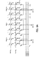
- FIGS. 6A-6C are a schematic representation showing part of an active matrix display module and details of the inventive selection scheme and the steps carried out during a third frame;
- FIGS. 7A-7C are a schematic representation showing part of an active matrix display module and details of the inventive selection scheme and the steps carried out during a fourth frame;
- FIGS. 8A-8F are a schematic representation showing part of an active matrix display module and details of the inventive selection scheme and the steps carried out during a first frame;
- FIGS. 9A-9F are a schematic representation showing part of an active matrix display module and details of the inventive selection scheme and the steps carried out during a second frame.
- the color shift is compensated by a smart selection order employed when selecting the sub-pixels. This is done within two frames.
- the color shift is partially compensated, and in the second frame completely. In this way, flicker (which might be present in the prior art solution) is avoided.
- the inventive selection order proposed herein is also chosen to minimize power consumption.
- the display panel 11 comprises pixels consisting of three sub-pixels (R n , G n , B n ).
- the sub-pixels are arranged in rows where the row line (horizontal) is called gate line.
- Each sub-pixel comprises a sub-pixel selection transistor 23 arranged at an intersection of a row and a column.
- the sub-pixel selection transistors 23 in a row are all connected to individual, i.e. different, data lines (vertical/column lines).
- a gate driver 12 is employed to select and deselect all pixels of a row of the display panel 11 .
- a source driver 20 provides the required voltage levels to all sub-pixels of a currently selected row of said display panel 11 , said voltage levels corresponding to the desired intensity for each color.
- the corresponding demultiplexer switches may be integrated onto the display panel 11 for demultiplexing the data lines of the display panel 11 .
- one demultiplexer switch is denoted as 21 . 1 .
- the control circuit 18 may comprise a demultiplexer logic or a sequencer to control the demultiplexer switches 21 in accordance with the present invention. That is, the control circuit 18 provides the right signals in order to switch the demultiplexer switches 21 so that the above-identified properties are satisfied.
- a first embodiment of the invention is designed for a multiplexing rate (mux rate) of 1:3.
- multiplex rate 1:3.
- the above-mentioned properties 1, 2, and 3 are being used. It is to be noted that according to the invention other selection orders than described here are possible too.
- FIGS. 4C and 5C show that the color shifts ⁇ B and ⁇ R are compensated by averaging over frame 1 and frame 2 (see the above-mentioned property 3).
- step 8 (carried out during the 3 rd and 4 th frame) is optional.
- a second embodiment of the invention is designed for a multiplexing rate (mux rate) of 1:6.
- the above-mentioned properties 1, 3, and 4 are being used. It is to be noted that according to the invention other selection orders than described here are possible too.
- the 1 st frame is then completed.
- a color shift (respectively ⁇ 1 to ⁇ 5 ) will appear on some sub-pixels, as shown in FIGS. 8D through 8F .
- each sub-pixel may be averaged out to 0V. This is realized in four frames. However, the color shift is partially compensated in each frame and completely over two frames, i.e. over frame 1 to frame 2 and over frame 3 to frame 4 , respectively.
- the selection order for the selection of the sub-pixels is typically implemented inside the control circuit 18 .
- This control circuit 18 provides the appropriate selection signals taking into account two or more of the properties 1 through 4 identified above.
- the present invention is intended to be used in LCD drivers where the source lines are multiplexed.
- Very well suited is the present invention for small displays, such as the ones used in mobile phones, PDAs, and the like.
Applications Claiming Priority (4)
| Application Number | Priority Date | Filing Date | Title |
|---|---|---|---|
| EP05112275 | 2005-12-16 | ||
| EP05112275.2 | 2005-12-16 | ||
| EP05112275 | 2005-12-16 | ||
| PCT/IB2006/054693 WO2007069159A2 (en) | 2005-12-16 | 2006-12-08 | Apparatus and method for color shift compensation in displays |
Publications (2)
| Publication Number | Publication Date |
|---|---|
| US20100013864A1 US20100013864A1 (en) | 2010-01-21 |
| US8619016B2 true US8619016B2 (en) | 2013-12-31 |
Family
ID=38042576
Family Applications (1)
| Application Number | Title | Priority Date | Filing Date |
|---|---|---|---|
| US12/097,638 Expired - Fee Related US8619016B2 (en) | 2005-12-16 | 2006-12-08 | Apparatus and method for color shift compensation in displays |
Country Status (7)
| Country | Link |
|---|---|
| US (1) | US8619016B2 (ja) |
| EP (1) | EP1964100B1 (ja) |
| JP (1) | JP5264499B2 (ja) |
| CN (1) | CN101331535A (ja) |
| AT (1) | ATE506672T1 (ja) |
| DE (1) | DE602006021473D1 (ja) |
| WO (1) | WO2007069159A2 (ja) |
Cited By (2)
| Publication number | Priority date | Publication date | Assignee | Title |
|---|---|---|---|---|
| US20160189640A1 (en) * | 2014-12-24 | 2016-06-30 | Shenzhen China Star Optoelectronics Technology Co. Ltd. | Driving circuits of liquid crystal panel and liquid crystal devices |
| US10311773B2 (en) * | 2013-07-26 | 2019-06-04 | Darwin Hu | Circuitry for increasing perceived display resolutions from an input image |
Families Citing this family (15)
| Publication number | Priority date | Publication date | Assignee | Title |
|---|---|---|---|---|
| US7839414B2 (en) | 2007-07-30 | 2010-11-23 | Motorola Mobility, Inc. | Methods and devices for display color compensation |
| KR101117736B1 (ko) | 2010-02-05 | 2012-02-27 | 삼성모바일디스플레이주식회사 | 디스플레이 장치 |
| TWI497477B (zh) * | 2010-05-13 | 2015-08-21 | Novatek Microelectronics Corp | 驅動模組與驅動方法 |
| CN102376281A (zh) * | 2010-08-23 | 2012-03-14 | 联咏科技股份有限公司 | 驱动模块与驱动方法 |
| US9230496B2 (en) * | 2011-01-24 | 2016-01-05 | Sharp Kabushiki Kaisha | Display device and method of driving the same |
| KR101829777B1 (ko) * | 2011-03-09 | 2018-02-20 | 삼성디스플레이 주식회사 | 광 감지 센서 |
| WO2012133281A1 (ja) * | 2011-03-31 | 2012-10-04 | シャープ株式会社 | 表示装置 |
| CN103927978A (zh) * | 2013-12-31 | 2014-07-16 | 厦门天马微电子有限公司 | Amoled显示面板及有机发光显示装置 |
| CN105096867B (zh) * | 2015-08-07 | 2018-04-10 | 深圳市华星光电技术有限公司 | 一种液晶显示器及其控制方法 |
| KR102509164B1 (ko) * | 2016-09-29 | 2023-03-13 | 엘지디스플레이 주식회사 | 표시장치 및 그를 이용한 서브픽셀 트랜지션 방법 |
| CN206194295U (zh) * | 2016-11-15 | 2017-05-24 | 京东方科技集团股份有限公司 | 数据线多路分配器、显示基板、显示面板及显示装置 |
| EP3549124B1 (fr) * | 2016-12-01 | 2023-07-12 | LRX Investissement | Mode d'adressage et principe de réalisation d'écrans matriciels d'affichage d'images couleur a comportement quasi-statique |
| US10726796B2 (en) * | 2018-05-30 | 2020-07-28 | Wuhan China Star Optoelectronics Technology Co., Ltd. | Backlight drive circuit, driving method thereof, and display device |
| CN110111755A (zh) * | 2019-06-18 | 2019-08-09 | 厦门天马微电子有限公司 | 一种显示面板、其驱动方法及显示装置 |
| CN116092405A (zh) * | 2022-12-12 | 2023-05-09 | 北京京东方技术开发有限公司 | 显示面板、显示驱动方法、显示驱动模组和显示装置 |
Citations (7)
| Publication number | Priority date | Publication date | Assignee | Title |
|---|---|---|---|---|
| JP2001324963A (ja) | 2000-05-15 | 2001-11-22 | Toshiba Corp | 表示装置 |
| US20010050665A1 (en) | 2000-06-08 | 2001-12-13 | Lg. Philips Lcd Co., Ltd | Liquid crystal display and driving method thereof |
| US20050035934A1 (en) | 2003-08-14 | 2005-02-17 | Toshiba Matsushita Display Technology Co., Ltd. | Liquid crystal display device |
| CN1617016A (zh) | 2003-11-10 | 2005-05-18 | 恩益禧电子股份有限公司 | 能抑制色差的公共反转驱动型液晶显示设备及其驱动方法 |
| JP2005250065A (ja) | 2004-03-03 | 2005-09-15 | Nec Electronics Corp | ディスプレイパネル駆動方法,ドライバ,及びディスプレイパネル駆動用プログラム |
| US20050200788A1 (en) * | 2002-09-23 | 2005-09-15 | Edwards Martin J. | Active matrix display devices |
| US20050280621A1 (en) * | 2001-04-27 | 2005-12-22 | Sanyo Electric Co., Ltd. | Active matrix display device |
Family Cites Families (2)
| Publication number | Priority date | Publication date | Assignee | Title |
|---|---|---|---|---|
| KR100675320B1 (ko) * | 2000-12-29 | 2007-01-26 | 엘지.필립스 엘시디 주식회사 | 액정표시장치의 구동방법 |
| JP2003058119A (ja) * | 2001-08-09 | 2003-02-28 | Sharp Corp | アクティブマトリクス型表示装置及びその駆動方法、並びにそれに備えられる駆動制御回路 |
-
2006
- 2006-12-08 JP JP2008545192A patent/JP5264499B2/ja not_active Expired - Fee Related
- 2006-12-08 US US12/097,638 patent/US8619016B2/en not_active Expired - Fee Related
- 2006-12-08 DE DE602006021473T patent/DE602006021473D1/de active Active
- 2006-12-08 WO PCT/IB2006/054693 patent/WO2007069159A2/en active Application Filing
- 2006-12-08 AT AT06832166T patent/ATE506672T1/de not_active IP Right Cessation
- 2006-12-08 EP EP06832166A patent/EP1964100B1/en not_active Not-in-force
- 2006-12-08 CN CNA2006800471018A patent/CN101331535A/zh active Pending
Patent Citations (8)
| Publication number | Priority date | Publication date | Assignee | Title |
|---|---|---|---|---|
| JP2001324963A (ja) | 2000-05-15 | 2001-11-22 | Toshiba Corp | 表示装置 |
| US20010050665A1 (en) | 2000-06-08 | 2001-12-13 | Lg. Philips Lcd Co., Ltd | Liquid crystal display and driving method thereof |
| US20050280621A1 (en) * | 2001-04-27 | 2005-12-22 | Sanyo Electric Co., Ltd. | Active matrix display device |
| US20050200788A1 (en) * | 2002-09-23 | 2005-09-15 | Edwards Martin J. | Active matrix display devices |
| US20050035934A1 (en) | 2003-08-14 | 2005-02-17 | Toshiba Matsushita Display Technology Co., Ltd. | Liquid crystal display device |
| US20050140633A1 (en) * | 2003-10-11 | 2005-06-30 | Nec Electronics Corporation | Common inversion driving type liquid crystal display device and its driving method capable of suppressing color errors |
| CN1617016A (zh) | 2003-11-10 | 2005-05-18 | 恩益禧电子股份有限公司 | 能抑制色差的公共反转驱动型液晶显示设备及其驱动方法 |
| JP2005250065A (ja) | 2004-03-03 | 2005-09-15 | Nec Electronics Corp | ディスプレイパネル駆動方法,ドライバ,及びディスプレイパネル駆動用プログラム |
Cited By (3)
| Publication number | Priority date | Publication date | Assignee | Title |
|---|---|---|---|---|
| US10311773B2 (en) * | 2013-07-26 | 2019-06-04 | Darwin Hu | Circuitry for increasing perceived display resolutions from an input image |
| US20160189640A1 (en) * | 2014-12-24 | 2016-06-30 | Shenzhen China Star Optoelectronics Technology Co. Ltd. | Driving circuits of liquid crystal panel and liquid crystal devices |
| US9672776B2 (en) * | 2014-12-24 | 2017-06-06 | Shenzhen China Star Optoelectronics Technology Co., Ltd | Driving circuits of liquid crystal panel and liquid crystal devices |
Also Published As
| Publication number | Publication date |
|---|---|
| JP2009519492A (ja) | 2009-05-14 |
| EP1964100B1 (en) | 2011-04-20 |
| US20100013864A1 (en) | 2010-01-21 |
| CN101331535A (zh) | 2008-12-24 |
| DE602006021473D1 (de) | 2011-06-01 |
| JP5264499B2 (ja) | 2013-08-14 |
| WO2007069159A3 (en) | 2007-09-13 |
| WO2007069159A2 (en) | 2007-06-21 |
| EP1964100A2 (en) | 2008-09-03 |
| ATE506672T1 (de) | 2011-05-15 |
Similar Documents
| Publication | Publication Date | Title |
|---|---|---|
| US8619016B2 (en) | Apparatus and method for color shift compensation in displays | |
| KR101318043B1 (ko) | 액정표시장치 및 그 구동방법 | |
| US8681081B2 (en) | Active matrix type display device and drive control circuit used in the same | |
| KR101245944B1 (ko) | 액정패널, 이를 구비한 액정표시장치 및 그 구동 방법 | |
| JP4140779B2 (ja) | 液晶パネルの駆動装置及びその駆動方法 | |
| KR101252854B1 (ko) | 액정 패널, 데이터 드라이버, 이를 구비한 액정표시장치 및그 구동 방법 | |
| US20100315402A1 (en) | Display panel driving method, gate driver, and display apparatus | |
| US20040017344A1 (en) | Liquid-crystal display device and driving method thereof | |
| US20080129904A1 (en) | Liquid crystal display and driving method thereof | |
| US8416175B2 (en) | Liquid crystal display device and method for driving the same | |
| US20090146938A1 (en) | Display device | |
| US8299998B2 (en) | Liquid crystal display device with first and second image signals about a middle voltage | |
| JP2010102189A (ja) | 液晶表示装置及びその駆動方法 | |
| KR20000059665A (ko) | 액정표시장치의 구동방법 | |
| US7365726B2 (en) | Method and circuit for driving liquid crystal display | |
| JP4062766B2 (ja) | 電子機器および表示装置 | |
| US20080088615A1 (en) | Driving method for liquid crystal display using block cycle inversion | |
| US20100103086A1 (en) | Liquid crystal display panel for performing polarity inversion therein | |
| WO2007069205A2 (en) | Apparatus and method for color shift compensation in displays | |
| JP2005182052A (ja) | インパルシブ駆動液晶表示装置及びその駆動方法 | |
| KR100965587B1 (ko) | 액정표시장치 및 이의 구동방법 | |
| KR100956343B1 (ko) | 액정 표시 장치 및 그 구동 방법 | |
| KR20150078567A (ko) | 액정표시장치 | |
| US20040207591A1 (en) | Method and circuit for driving liquid crystal display | |
| KR20070070639A (ko) | 표시 장치의 구동 장치 |
Legal Events
| Date | Code | Title | Description |
|---|---|---|---|
| AS | Assignment |
Owner name: NXP B.V.,NETHERLANDS Free format text: ASSIGNMENT OF ASSIGNORS INTEREST;ASSIGNORS:OELHAFEN, PATRICK;BRUNNER, PATRICK;SIGNING DATES FROM 20070724 TO 20070821;REEL/FRAME:022118/0177 Owner name: NXP B.V., NETHERLANDS Free format text: ASSIGNMENT OF ASSIGNORS INTEREST;ASSIGNORS:OELHAFEN, PATRICK;BRUNNER, PATRICK;SIGNING DATES FROM 20070724 TO 20070821;REEL/FRAME:022118/0177 |
|
| AS | Assignment |
Owner name: NXP HOLDING 1 B.V.,NETHERLANDS Free format text: ASSIGNMENT OF ASSIGNORS INTEREST;ASSIGNOR:NXP;REEL/FRAME:023928/0489 Effective date: 20100207 Owner name: TRIDENT MICROSYSTEMS (FAR EAST) LTD.,CAYMAN ISLAND Free format text: ASSIGNMENT OF ASSIGNORS INTEREST;ASSIGNORS:TRIDENT MICROSYSTEMS (EUROPE) B.V.;NXP HOLDING 1 B.V.;REEL/FRAME:023928/0641 Effective date: 20100208 Owner name: TRIDENT MICROSYSTEMS (FAR EAST) LTD., CAYMAN ISLAN Free format text: ASSIGNMENT OF ASSIGNORS INTEREST;ASSIGNORS:TRIDENT MICROSYSTEMS (EUROPE) B.V.;NXP HOLDING 1 B.V.;REEL/FRAME:023928/0641 Effective date: 20100208 Owner name: NXP HOLDING 1 B.V., NETHERLANDS Free format text: ASSIGNMENT OF ASSIGNORS INTEREST;ASSIGNOR:NXP;REEL/FRAME:023928/0489 Effective date: 20100207 |
|
| AS | Assignment |
Owner name: ENTROPIC COMMUNICATIONS, INC., CALIFORNIA Free format text: ASSIGNMENT OF ASSIGNORS INTEREST;ASSIGNORS:TRIDENT MICROSYSTEMS, INC.;TRIDENT MICROSYSTEMS (FAR EAST) LTD.;REEL/FRAME:028146/0178 Effective date: 20120411 |
|
| FEPP | Fee payment procedure |
Free format text: PAYOR NUMBER ASSIGNED (ORIGINAL EVENT CODE: ASPN); ENTITY STATUS OF PATENT OWNER: LARGE ENTITY |
|
| STCF | Information on status: patent grant |
Free format text: PATENTED CASE |
|
| AS | Assignment |
Owner name: ENTROPIC COMMUNICATIONS, INC., CALIFORNIA Free format text: MERGER AND CHANGE OF NAME;ASSIGNORS:EXCALIBUR ACQUISITION CORPORATION;ENTROPIC COMMUNICATIONS, INC.;ENTROPIC COMMUNICATIONS, INC.;REEL/FRAME:035706/0267 Effective date: 20150430 |
|
| AS | Assignment |
Owner name: ENTROPIC COMMUNICATIONS, LLC, CALIFORNIA Free format text: MERGER AND CHANGE OF NAME;ASSIGNORS:ENTROPIC COMMUNICATIONS, INC.;EXCALIBUR SUBSIDIARY, LLC;ENTROPIC COMMUNICATIONS, LLC;REEL/FRAME:035717/0628 Effective date: 20150430 |
|
| AS | Assignment |
Owner name: MORGAN STANLEY SENIOR FUNDING, INC., MARYLAND Free format text: SECURITY AGREEMENT SUPPLEMENT;ASSIGNOR:NXP B.V.;REEL/FRAME:038017/0058 Effective date: 20160218 |
|
| AS | Assignment |
Owner name: MORGAN STANLEY SENIOR FUNDING, INC., MARYLAND Free format text: CORRECTIVE ASSIGNMENT TO CORRECT THE REMOVE APPLICATION 12092129 PREVIOUSLY RECORDED ON REEL 038017 FRAME 0058. ASSIGNOR(S) HEREBY CONFIRMS THE SECURITY AGREEMENT SUPPLEMENT;ASSIGNOR:NXP B.V.;REEL/FRAME:039361/0212 Effective date: 20160218 |
|
| AS | Assignment |
Owner name: NXP B.V., NETHERLANDS Free format text: PATENT RELEASE;ASSIGNOR:MORGAN STANLEY SENIOR FUNDING, INC.;REEL/FRAME:039707/0471 Effective date: 20160805 |
|
| AS | Assignment |
Owner name: MORGAN STANLEY SENIOR FUNDING, INC., MARYLAND Free format text: CORRECTIVE ASSIGNMENT TO CORRECT THE REMOVE APPLICATION 12681366 PREVIOUSLY RECORDED ON REEL 039361 FRAME 0212. ASSIGNOR(S) HEREBY CONFIRMS THE SECURITY AGREEMENT SUPPLEMENT;ASSIGNOR:NXP B.V.;REEL/FRAME:042762/0145 Effective date: 20160218 Owner name: MORGAN STANLEY SENIOR FUNDING, INC., MARYLAND Free format text: CORRECTIVE ASSIGNMENT TO CORRECT THE REMOVE APPLICATION 12681366 PREVIOUSLY RECORDED ON REEL 038017 FRAME 0058. ASSIGNOR(S) HEREBY CONFIRMS THE SECURITY AGREEMENT SUPPLEMENT;ASSIGNOR:NXP B.V.;REEL/FRAME:042985/0001 Effective date: 20160218 |
|
| AS | Assignment |
Owner name: JPMORGAN CHASE BANK, N.A., AS COLLATERAL AGENT, IL Free format text: SECURITY AGREEMENT;ASSIGNORS:MAXLINEAR, INC.;ENTROPIC COMMUNICATIONS, LLC (F/K/A ENTROPIC COMMUNICATIONS, INC.);EXAR CORPORATION;REEL/FRAME:042453/0001 Effective date: 20170512 Owner name: JPMORGAN CHASE BANK, N.A., AS COLLATERAL AGENT, ILLINOIS Free format text: SECURITY AGREEMENT;ASSIGNORS:MAXLINEAR, INC.;ENTROPIC COMMUNICATIONS, LLC (F/K/A ENTROPIC COMMUNICATIONS, INC.);EXAR CORPORATION;REEL/FRAME:042453/0001 Effective date: 20170512 |
|
| FPAY | Fee payment |
Year of fee payment: 4 |
|
| AS | Assignment |
Owner name: DYNAMIC DATA TECHNOLOGIES LLC, MINNESOTA Free format text: ASSIGNMENT OF ASSIGNORS INTEREST;ASSIGNORS:MAXLINEAR INC.;ENTROPIC COMMUNICATIONS LLC;REEL/FRAME:047914/0274 Effective date: 20180418 |
|
| AS | Assignment |
Owner name: NXP B.V., NETHERLANDS Free format text: RELEASE BY SECURED PARTY;ASSIGNOR:MORGAN STANLEY SENIOR FUNDING, INC.;REEL/FRAME:050745/0001 Effective date: 20190903 |
|
| AS | Assignment |
Owner name: MORGAN STANLEY SENIOR FUNDING, INC., MARYLAND Free format text: CORRECTIVE ASSIGNMENT TO CORRECT THE REMOVE APPLICATION 12298143 PREVIOUSLY RECORDED ON REEL 042762 FRAME 0145. ASSIGNOR(S) HEREBY CONFIRMS THE SECURITY AGREEMENT SUPPLEMENT;ASSIGNOR:NXP B.V.;REEL/FRAME:051145/0184 Effective date: 20160218 Owner name: MORGAN STANLEY SENIOR FUNDING, INC., MARYLAND Free format text: CORRECTIVE ASSIGNMENT TO CORRECT THE REMOVE APPLICATION 12298143 PREVIOUSLY RECORDED ON REEL 039361 FRAME 0212. ASSIGNOR(S) HEREBY CONFIRMS THE SECURITY AGREEMENT SUPPLEMENT;ASSIGNOR:NXP B.V.;REEL/FRAME:051029/0387 Effective date: 20160218 Owner name: MORGAN STANLEY SENIOR FUNDING, INC., MARYLAND Free format text: CORRECTIVE ASSIGNMENT TO CORRECT THE REMOVE APPLICATION 12298143 PREVIOUSLY RECORDED ON REEL 042985 FRAME 0001. ASSIGNOR(S) HEREBY CONFIRMS THE SECURITY AGREEMENT SUPPLEMENT;ASSIGNOR:NXP B.V.;REEL/FRAME:051029/0001 Effective date: 20160218 Owner name: MORGAN STANLEY SENIOR FUNDING, INC., MARYLAND Free format text: CORRECTIVE ASSIGNMENT TO CORRECT THE REMOVE APPLICATION 12298143 PREVIOUSLY RECORDED ON REEL 038017 FRAME 0058. ASSIGNOR(S) HEREBY CONFIRMS THE SECURITY AGREEMENT SUPPLEMENT;ASSIGNOR:NXP B.V.;REEL/FRAME:051030/0001 Effective date: 20160218 Owner name: MORGAN STANLEY SENIOR FUNDING, INC., MARYLAND Free format text: CORRECTIVE ASSIGNMENT TO CORRECT THE REMOVE APPLICATION12298143 PREVIOUSLY RECORDED ON REEL 039361 FRAME 0212. ASSIGNOR(S) HEREBY CONFIRMS THE SECURITY AGREEMENT SUPPLEMENT;ASSIGNOR:NXP B.V.;REEL/FRAME:051029/0387 Effective date: 20160218 Owner name: MORGAN STANLEY SENIOR FUNDING, INC., MARYLAND Free format text: CORRECTIVE ASSIGNMENT TO CORRECT THE REMOVE APPLICATION12298143 PREVIOUSLY RECORDED ON REEL 042985 FRAME 0001. ASSIGNOR(S) HEREBY CONFIRMS THE SECURITY AGREEMENT SUPPLEMENT;ASSIGNOR:NXP B.V.;REEL/FRAME:051029/0001 Effective date: 20160218 Owner name: MORGAN STANLEY SENIOR FUNDING, INC., MARYLAND Free format text: CORRECTIVE ASSIGNMENT TO CORRECT THE REMOVE APPLICATION12298143 PREVIOUSLY RECORDED ON REEL 042762 FRAME 0145. ASSIGNOR(S) HEREBY CONFIRMS THE SECURITY AGREEMENT SUPPLEMENT;ASSIGNOR:NXP B.V.;REEL/FRAME:051145/0184 Effective date: 20160218 |
|
| AS | Assignment |
Owner name: MUFG UNION BANK, N.A., CALIFORNIA Free format text: SUCCESSION OF AGENCY (REEL 042453 / FRAME 0001);ASSIGNOR:JPMORGAN CHASE BANK, N.A.;REEL/FRAME:053115/0842 Effective date: 20200701 |
|
| AS | Assignment |
Owner name: MAXLINEAR, INC., CALIFORNIA Free format text: RELEASE BY SECURED PARTY;ASSIGNOR:MUFG UNION BANK, N.A.;REEL/FRAME:056656/0204 Effective date: 20210623 Owner name: EXAR CORPORATION, CALIFORNIA Free format text: RELEASE BY SECURED PARTY;ASSIGNOR:MUFG UNION BANK, N.A.;REEL/FRAME:056656/0204 Effective date: 20210623 Owner name: MAXLINEAR COMMUNICATIONS LLC, CALIFORNIA Free format text: RELEASE BY SECURED PARTY;ASSIGNOR:MUFG UNION BANK, N.A.;REEL/FRAME:056656/0204 Effective date: 20210623 |
|
| FEPP | Fee payment procedure |
Free format text: MAINTENANCE FEE REMINDER MAILED (ORIGINAL EVENT CODE: REM.); ENTITY STATUS OF PATENT OWNER: LARGE ENTITY |
|
| LAPS | Lapse for failure to pay maintenance fees |
Free format text: PATENT EXPIRED FOR FAILURE TO PAY MAINTENANCE FEES (ORIGINAL EVENT CODE: EXP.); ENTITY STATUS OF PATENT OWNER: LARGE ENTITY |
|
| STCH | Information on status: patent discontinuation |
Free format text: PATENT EXPIRED DUE TO NONPAYMENT OF MAINTENANCE FEES UNDER 37 CFR 1.362 |
|
| FP | Lapsed due to failure to pay maintenance fee |
Effective date: 20211231 |