US8604488B2 - Light emitting diode and fabricating method thereof - Google Patents
Light emitting diode and fabricating method thereof Download PDFInfo
- Publication number
- US8604488B2 US8604488B2 US13/365,217 US201213365217A US8604488B2 US 8604488 B2 US8604488 B2 US 8604488B2 US 201213365217 A US201213365217 A US 201213365217A US 8604488 B2 US8604488 B2 US 8604488B2
- Authority
- US
- United States
- Prior art keywords
- gan substrate
- led
- light emitting
- semiconductor layer
- type semiconductor
- Prior art date
- Legal status (The legal status is an assumption and is not a legal conclusion. Google has not performed a legal analysis and makes no representation as to the accuracy of the status listed.)
- Active, expires
Links
- 238000000034 method Methods 0.000 title description 20
- JMASRVWKEDWRBT-UHFFFAOYSA-N Gallium nitride Chemical compound [Ga]#N JMASRVWKEDWRBT-UHFFFAOYSA-N 0.000 claims abstract description 169
- 239000004065 semiconductor Substances 0.000 claims abstract description 67
- 239000000758 substrate Substances 0.000 claims description 17
- 150000004767 nitrides Chemical class 0.000 claims description 5
- 238000000605 extraction Methods 0.000 description 23
- 229910002601 GaN Inorganic materials 0.000 description 18
- 229910052594 sapphire Inorganic materials 0.000 description 13
- 239000010980 sapphire Substances 0.000 description 13
- 238000002834 transmittance Methods 0.000 description 13
- 230000008569 process Effects 0.000 description 11
- 230000000694 effects Effects 0.000 description 9
- 238000005530 etching Methods 0.000 description 8
- 238000010586 diagram Methods 0.000 description 7
- 230000004888 barrier function Effects 0.000 description 5
- 230000002708 enhancing effect Effects 0.000 description 5
- 230000002349 favourable effect Effects 0.000 description 5
- 239000000463 material Substances 0.000 description 5
- 238000004088 simulation Methods 0.000 description 5
- 239000000243 solution Substances 0.000 description 5
- 238000002474 experimental method Methods 0.000 description 4
- 238000004519 manufacturing process Methods 0.000 description 4
- 238000002347 injection Methods 0.000 description 3
- 239000007924 injection Substances 0.000 description 3
- 238000004020 luminiscence type Methods 0.000 description 3
- 238000001039 wet etching Methods 0.000 description 3
- QAOWNCQODCNURD-UHFFFAOYSA-N Sulfuric acid Chemical compound OS(O)(=O)=O QAOWNCQODCNURD-UHFFFAOYSA-N 0.000 description 2
- 238000010521 absorption reaction Methods 0.000 description 2
- 238000004364 calculation method Methods 0.000 description 2
- 239000002019 doping agent Substances 0.000 description 2
- 230000031700 light absorption Effects 0.000 description 2
- 238000012986 modification Methods 0.000 description 2
- 230000004048 modification Effects 0.000 description 2
- 230000003287 optical effect Effects 0.000 description 2
- GYHNNYVSQQEPJS-UHFFFAOYSA-N Gallium Chemical compound [Ga] GYHNNYVSQQEPJS-UHFFFAOYSA-N 0.000 description 1
- 230000008901 benefit Effects 0.000 description 1
- 150000001875 compounds Chemical class 0.000 description 1
- 230000007423 decrease Effects 0.000 description 1
- 230000007547 defect Effects 0.000 description 1
- 230000005611 electricity Effects 0.000 description 1
- 238000000407 epitaxy Methods 0.000 description 1
- 230000001747 exhibiting effect Effects 0.000 description 1
- 229910052733 gallium Inorganic materials 0.000 description 1
- 230000017525 heat dissipation Effects 0.000 description 1
- 238000005259 measurement Methods 0.000 description 1
- 238000005498 polishing Methods 0.000 description 1
- 230000009467 reduction Effects 0.000 description 1
- 239000012780 transparent material Substances 0.000 description 1
- 239000002699 waste material Substances 0.000 description 1
- 230000003313 weakening effect Effects 0.000 description 1
Images


Classifications
-
- H—ELECTRICITY
- H01—ELECTRIC ELEMENTS
- H01L—SEMICONDUCTOR DEVICES NOT COVERED BY CLASS H10
- H01L33/00—Semiconductor devices having potential barriers specially adapted for light emission; Processes or apparatus specially adapted for the manufacture or treatment thereof or of parts thereof; Details thereof
- H01L33/02—Semiconductor devices having potential barriers specially adapted for light emission; Processes or apparatus specially adapted for the manufacture or treatment thereof or of parts thereof; Details thereof characterised by the semiconductor bodies
- H01L33/20—Semiconductor devices having potential barriers specially adapted for light emission; Processes or apparatus specially adapted for the manufacture or treatment thereof or of parts thereof; Details thereof characterised by the semiconductor bodies with a particular shape, e.g. curved or truncated substrate
- H01L33/22—Roughened surfaces, e.g. at the interface between epitaxial layers
-
- H—ELECTRICITY
- H01—ELECTRIC ELEMENTS
- H01L—SEMICONDUCTOR DEVICES NOT COVERED BY CLASS H10
- H01L33/00—Semiconductor devices having potential barriers specially adapted for light emission; Processes or apparatus specially adapted for the manufacture or treatment thereof or of parts thereof; Details thereof
- H01L33/005—Processes
- H01L33/0062—Processes for devices with an active region comprising only III-V compounds
- H01L33/0075—Processes for devices with an active region comprising only III-V compounds comprising nitride compounds
-
- H—ELECTRICITY
- H01—ELECTRIC ELEMENTS
- H01L—SEMICONDUCTOR DEVICES NOT COVERED BY CLASS H10
- H01L33/00—Semiconductor devices having potential barriers specially adapted for light emission; Processes or apparatus specially adapted for the manufacture or treatment thereof or of parts thereof; Details thereof
- H01L33/005—Processes
- H01L33/0093—Wafer bonding; Removal of the growth substrate
Definitions
- the technical field relates to a light emitting diode (LED) and a fabricating method thereof, and particularly to an LED and a fabricating method thereof capable of enhancing a light extraction efficiency.
- LED light emitting diode
- a light emitting diode is a semiconductor device constituted mainly by, for example, group III-V compound semiconductor materials. Since such semiconductor materials have a characteristic of converting electricity into light, when a current is applied to the semiconductor materials, electrons therein are combined with holes and excessive energy are released in form of light, thereby achieving an effect of luminosity.
- Sapphire is often used as an epitaxy substrate in an LED, generally speaking. Since sapphire is a transparent material, an LED fabricated by using sapphire would scatter light to all directions without focusing the light and resulting in waste. Meanwhile, the scattered light is absorbed by each semiconductor layer inside the LED and heat is accumulated. Therefore, the emitting luminosity and efficiency of the gallium nitride (GaN) LEDs are lowered.
- GaN gallium nitride
- the GaN serving as the material for the epitaxial layer in the LED and sapphire substrates have mismatching lattice constants of around 16%, a large quantity of defects occurs at lattice growth junction, thus drastically weakening the luminous intensity.
- the sapphire substrates adopted in conventional LEDs have lower heat dissipation coefficients than the GaN substrates, therefore due to the heat buildup, the luminous intensity is easily reduced.
- the low light extraction efficiency causes drastic reduction in the external quantum efficiency of the LED, and accordingly the industry is earnestly pursuing an LED with high light extraction efficiency.
- the disclosure is directed to a light emitting diode (LED) capable of adjusting a total reflection angle of light to enhance a light extraction efficiency.
- LED light emitting diode
- An LED including a gallium nitride (GaN) substrate, a first type semiconductor layer, a light emitting layer, a second type semiconductor layer, a first electrode, and a second electrode.
- the GaN substrate includes a first surface and a second surface, in which the first surface and the second surface are disposed on two sides of the GaN substrate, and the second surface has a plurality of protuberances.
- a height of the protuberances is h ⁇ m
- a distribution density of the protuberances on the second surface is d cm ⁇ 2 , in which h 2 d ⁇ 9.87 ⁇ 10 7 , and h ⁇ 1.8.
- the first type semiconductor layer is disposed on the first surface of the GaN substrate.
- the light emitting layer is disposed on a partial portion of the first type semiconductor layer, and a wavelength of a light emitted by the light emitting layer is from 375 nm to 415 nm.
- the second type semiconductor layer is disposed on the light emitting layer.
- the first electrode is disposed on a partial region of the first type semiconductor layer, and the second electrode is disposed on a partial region of the second type semiconductor layer.
- the GaN substrate includes a first surface and a second surface, in which the first surface and the second surface are disposed on two sides of the GaN substrate, and the second surface has a plurality of protuberances.
- a height of the protuberances is h ⁇ m
- a distribution density of the protuberances on the second surface is d cm ⁇ 2 , in which h 2 d ⁇ 9.87 ⁇ 10 7 , and d ⁇ 8 ⁇ 10 8 .
- the first type semiconductor layer is disposed on the first surface of the GaN substrate.
- the light emitting layer is disposed on a partial portion of the first type semiconductor layer, and a wavelength of a light emitted by the light emitting layer is from 375 nm to 415 nm.
- the second type semiconductor layer is disposed on the light emitting layer.
- the first electrode is disposed on a partial region of the first type semiconductor layer, and the second electrode is disposed on a partial region of the second type semiconductor layer.
- the GaN substrate includes a first surface and a second surface, in which the first surface and the second surface are disposed on two sides of the GaN substrate, and the second surface has a plurality of protuberances.
- a height of the protuberances is h ⁇ m
- a distribution density of the protuberances on the second surface is d cm ⁇ 2 , in which 3 ⁇ h ⁇ 6, and 1.5 ⁇ 10 6 ⁇ d ⁇ 7.5 ⁇ 10 6 .
- the first type semiconductor layer is disposed on the first surface of the GaN substrate.
- the light emitting layer is disposed on a partial portion of the first type semiconductor layer, and a wavelength of a light emitted by the light emitting layer is from 375 nm to 415 nm.
- the second type semiconductor layer is disposed on the light emitting layer.
- the first electrode is disposed on a partial region of the first type semiconductor layer, and the second electrode is disposed on a partial region of the second type semiconductor layer.
- FIGS. 1A and 1B are schematic cross-sectional views respectively illustrating an LED according to an exemplary embodiment.
- FIG. 2A is a schematic cross-sectional view of a SQW light emitting layer in an LED according to an exemplary embodiment.
- FIG. 2B is a schematic cross-sectional view of a MQW light emitting layer in an LED according to an exemplary embodiment.
- FIGS. 3A-3E are schematic cross-sectional views of a fabricating process of an LED according to an exemplary embodiment.
- FIG. 4A illustrates a protuberance after the N-face of the GaN substrate has been etched.
- FIG. 4B is an schematic view for complementing the description of a calculation of a height of a protuberance on the N-face of the GaN substrate and a distribution density of the protuberances on the second surface.
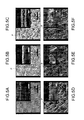
- FIGS. 5A-5F respectively illustrates experiments forming different types of protuberances on the GaN substrate according to an exemplary embodiment.
- FIGS. 6A-6C respectively illustrates simulation views of the far-field angle of an LED having different types of protuberances formed by different etch times according to an exemplary embodiment.
- FIG. 7 illustrates a relationship of the etch time relative to an injection current to the LED and the luminous intensity, according to an exemplary embodiment adopting second surfaces having different types of protuberances formed by different etch times.
- FIGS. 8A and 8B are optical performance diagrams of the far-field angle relative of an LED adopting the second surface having different types of protuberances formed by the different etch times listed in Table 2.
- FIGS. 9A and 9B are curve diagrams respectively illustrating the relationships of the GaN substrate in an LED relative to the wavelength and the transmittance according to an exemplary embodiment.
- FIGS. 1A and 1B are schematic cross-sectional views respectively illustrating an LED according to an exemplary embodiment.
- an LED 200 includes a GaN substrate 210 , a first type semiconductor layer 220 , a light emitting layer 230 , a second type semiconductor layer 240 , a first electrode 250 , and a second electrode 260 .
- the GaN substrate 210 has a first surface 210 A and a second surface 210 B, and in the present embodiment, the second surface 210 B is a nitride surface of the GaN substrate 210 , for example.
- the first type semiconductor layer 220 , the light emitting layer 230 , and the second type semiconductor layer 240 are stacked in sequence on the first surface 210 A of the GaN substrate 210 .
- the first type semiconductor layer 220 is disposed on the first surface 210 A of the GaN substrate 210 , and the light emitting layer 230 is disposed on a partial region of the first type semiconductor layer 220 .
- the second type semiconductor layer 240 is disposed on the light emitting layer 230 .
- the first electrode 250 is disposed on the partial region of the first type semiconductor layer 220 to electrically connect to the first type semiconductor layer 220 .
- the second electrode 260 is disposed on a partial region of the second type semiconductor layer 240 to electrically connect to the second type semiconductor layer 240 .
- a stacked pattern of the afore-described film layers may be as depicted in FIG.
- first electrodes 250 and the second electrodes 260 are respectively disposed on two opposite sides of the stacked layers constituted by the second type semiconductor layer 240 , the light emitting layer 230 , the first type semiconductor layer 220 , and the GaN substrate 210 .
- the first electrode 250 is disposed on the second surface 210 B of the GaN substrate 210 , although the disclosure is not limited thereto.
- the first type semiconductor layer 220 is an n-type semiconductor, for example, including an undoped GaN layer 220 a , a first n-type doped GaN layer 220 b , and a second n-type doped GaN layer 220 c stacked in sequence on the GaN substrate 210 .
- the first n-type doped GaN layer 220 b and the second n-type doped GaN layer 220 c may have different thicknesses or dopant concentrations.
- the second type semiconductor layer 240 may be a p-type semiconductor layer, for example, including a first p-type doped GaN layer 240 a and a second p-type doped GaN layer 240 b stacked in sequence on the light emitting layer 230 .
- the thickness or the dopant concentration of the first p-type doped GaN layer 240 a is different from the second p-type doped GaN layer 240 b.
- the light emitting layer 230 may be a single quantum well (SQW) light emitting layer 230 or a multiple quantum well (MQW) light emitting layer 230 .
- SQW single quantum well
- MQW multiple quantum well
- FIGS. 2A and 2B FIG. 2A is a schematic cross-sectional view of a SQW light emitting layer in an LED according to an exemplary embodiment
- FIG. 2B is a schematic cross-sectional view of a MQW light emitting layer in an LED according to an exemplary embodiment.
- FIG. 2A is a schematic cross-sectional view of a SQW light emitting layer in an LED according to an exemplary embodiment
- MQW multiple quantum well
- the SQW light emitting layer 230 may be formed by a plurality of quantum barrier layers 230 a and quantum wells 230 b , for example by stacking quantum barrier layer 230 a /quantum well 230 b /quantum barrier layer 230 a .
- a material of the quantum wells 230 b may be, for instance, Al x In y Ga 1-x-y N, in which 0 ⁇ x ⁇ 1 and 0 ⁇ y ⁇ 1, and persons skilled in the art may select the growth quantities of x and y based on practical requirements, so the disclosure is not limited thereto.
- the MQW light emitting layer 230 may be formed by at least two pairs of stacked quantum barrier layers 230 a and quantum wells 230 b , for example by repeatedly stacking quantum barrier layer 230 a /quantum well 230 b as depicted in FIG. 2B .
- a thickness of the GaN substrate 210 is between 70 nm to 120 nm, and the second surface 210 B has a plurality of protuberances P forming a rough surface. Accordingly, not only can the light absorption rate be reduced when light passes through the GaN substrate 210 , the total internal reflection effect generated at the second surface 210 B can also be lowered when light passes through the GaN substrate 210 , thereby enhancing the power of light.
- the second surface 210 B of the GaN substrate 210 having the plurality of protuberances P formed thereon is especially conducive to enhancing a power extraction of a particular wavelength. Specifically, an enhancement effect is especially noticeable for a wavelength range of 375 nm to 415 nm of the light emitted by the light emitting layer 230 .
- FIG. 1A schematic diagrams of a fabrication process of the LED 200 having the structure of the afore-described GaN substrate 210 are provided.
- laboratory results of a GaN substrate capable of implementing the aforementioned characteristics are provided, although the embodiments below do not limit the disclosure.
- FIGS. 3A-3E are schematic cross-sectional views of a fabricating process of an LED according to an exemplary embodiment.
- a GaN substrate 210 is provided, in which a gallium surface (Ga-face) of the GaN substrate 210 serves as the first surface 210 A for forming a predetermined device thereon.
- film layers such as the first type semiconductor layer 220 including the undoped GaN layer 220 a and the second n-type doped GaN layer 220 c , the light emitting layer 230 , and the second type semiconductor layer 240 are formed in sequence on the first surface 210 A of the GaN substrate 210 .
- FIG. 3C by using chip fabrication processes a plurality of LEDs 200 depicted in FIG.
- each of the LEDs 200 includes the GaN substrate 210 , the first type semiconductor layer 220 , the light emitting layer 230 , second type semiconductor layer 240 including the first p-type doped GaN layer 240 a and the second p-type doped GaN layer 240 b , the first electrode 250 , and the second electrode 260 .
- a fabrication technique can be employed for thinning the thickness of the GaN substrate 210 , so a thickness D 1 of the GaN substrate 210 is reduced to a thickness D 2 , in which the thickness D 2 after thinning the GaN substrate 210 is approximately between 70-120 ⁇ m.
- the method for thinning the thickness may be a mechanical polishing method or an etching method, for example. Accordingly, the absorption effect of the emitted light from the light emitting layer 230 when passing through the GaN substrate 210 can be initially lowered, thus enhancing the power extraction.
- the N-face (i.e., a predetermined forming surface 210 b of the second surface 210 B) of the GaN substrate 210 is etched by a wet etching technique, so as to form a plurality of protuberances P on the N-face of the GaN substrate 210 .
- the plurality of protuberances P on the second surface 210 B can be used to reduce the total internal reflection effect when light is emitted from the GaN substrate 210 interface, thereby further enhancing the power extraction.
- the detailed structures of the plurality of protuberances P formed on the second surface 210 B are described later.
- the GaN substrate 210 is divided to form a plurality of LEDs 200 with high power extraction. It should be obvious that, in another embodiment, the GaN substrate 210 may be first divided to form the plurality of LEDs 200 , and then the wet etching technique is performed on the divided GaN substrate 210 for thinning the thickness of the GaN substrate 210 so as to form the LED in the disclosure, although the fabrication process of the LED is not limited thereto in the disclosure.
- the power extraction and the luminous intensity of the LED 200 can be effectively enhanced by adjusting the plurality of protuberances P on the second surface 210 B of the GaN substrate 210 .
- the plurality of protuberances P formed on the second surface 210 B of the GaN substrate 210 after etching are sawtooth shaped pyramids, for instance.
- persons skilled in the art may select sulfuric acid or other etching solutions to perform the wet etch process.
- a height and a distribution density of the plurality of protuberances P on the second surface 210 B can be controlled.
- a total reflection angle of the emitted light from the LED can be effectively adjusted, and a preferable power extraction can be achieved.
- FIG. 4A illustrates a protuberance P having a pyramidal shape after the N-face of the GaN substrate has been etched.
- each of the formed pyramids displays a hexagonal pyramid shape, and a characteristic angle of 58 degrees is included between the apex and the bottom surface of each pyramid.
- the included angle between the pyramid apex and the bottom surface can be known to be 58 degrees according to the lattice arrangement of the N-face of the GaN substrate. Therefore, when the height of the protuberance is h ⁇ m, a height of one of the triangles forming the bottom surface is h ⁇ cot 58° ⁇ sin 60°. Moreover, a base of one of the triangles forming the bottom surface is (h ⁇ cot 58°) ⁇ cos 60° ⁇ 2.
- an area of the bottom surface of the pyramid can be calculated as a total area of six of the aforementioned triangles 6 ⁇ 1/2 ⁇ (h ⁇ cot 58° ⁇ sin 60°) ⁇ (2 ⁇ cos 60°) ⁇ (h ⁇ cot 58°), and therefore the area of the bottom surface of pyramid is 6 ⁇ h 2 ⁇ cot 2 58° ⁇ sin 60° cos 60°.
- the distribution density d cm ⁇ 2 of the pyramid can be derived by dividing the unit area by the area of the bottom surface of the pyramid.
- the above calculation is a theoretically calculated value based on the pyramids being arranged in a most sparse manner in the unit area. Therefore, the height h of the protuberances in the second surface and the distribution density d of the protuberances on the second surface should satisfy the condition: 9.87 ⁇ 10 7 ⁇ h 2 d.
- Table 1 lists a plurality of experiments for forming the second surface 210 B having the protuberances P on the GaN substrate 210 according to an exemplary embodiment. Moreover, Table 1 exhibits the etch time and the relationship of the vertical heights and the distribution density of the protuberances P formed after the etching.
- FIGS. 5A-5F are scanning electron microscope (SEM) measurement photos corresponding to each experiment in Table 1.
- FIG. 5A B 1 0.25 ⁇ 0.35 8 ⁇ 10 9 ⁇ 9 ⁇ 10 9
- FIG. 5B C 5 0.7 ⁇ 1.0 1 ⁇ 10 9 ⁇ 2 ⁇ 10 9
- FIG. 5C D 10 0.9 ⁇ 1.8 8 ⁇ 10 8 ⁇ 1.5 ⁇ 10 9
- FIG. 5D E 30 3.0 ⁇ 5.5 6.0 ⁇ 10 6 ⁇ 7.5 ⁇ 10 6
- FIG. 5E F 60 4.0 ⁇ 6.0 1.5 ⁇ 10 6 ⁇ 2.5 ⁇ 10 6
- FIG. 5F
- the distribution density of the plurality of protuberances P becomes more sparse as the etch time increased, and the height of the protuberances increases as the etch time increased.
- FIGS. 6A-6C respectively illustrates simulation views of the far-field angle of an LED having different types of protuberances formed by different etch times according to an exemplary embodiment.
- FIG. 6A is a far-field angle simulation view of the LED having the protuberances depicted in FIG. 5B with 1 minute etch time as shown in Table 1.
- FIG. 6B is a far-field angle simulation view of the LED having the protuberances depicted in FIG. 5D with 10 minute etch time as shown in Table 1.
- FIG. 6C is a far-field angle simulation view of the LED having the protuberances depicted in FIG. 5E with 30 minute etch time as shown in Table 1. As shown by FIGS.
- the LEDs in the disclosure achieves power extractions of 66.7%, 62.8%, and 51.5%, respectively. Accordingly, the LED in the disclosure has favorable power extraction, and the light extraction rate (power extraction) increases as the height of the pyramids decreases and the distribution density increases.
- FIG. 7 illustrates a relationship of the etch time relative to an injection current to the LED and the luminous intensity, according to an exemplary embodiment adopting second surfaces having different types of protuberances formed by different etch times.
- the horizontal axis of FIG. 7 represents different injection currents (units: amperes), the vertical axis represents the luminous intensity (units: watts), and the different line segments represent the different etch times executed.
- a KOH solution with a 2M concentration is used, the temperature is at least 55° C., for example 80° C., and the etch times are respectively 1, 10, and 30 minutes.
- Table 2 The results are tabulated in Table 2 below.
- the original luminous intensity of 13.1 mW when the emitted wavelength of the LED is 405 nm is increased approximately two times to 27.2 mW.
- an especially favorable luminous intensity results when the height of the protuberances P is between 250 nm to 350 nm and the distribution density is between 8 ⁇ 10 9 to 9 ⁇ 10 9 cm ⁇ 2 .
- FIGS. 8A and 8B are optical performance diagrams of the far-field angle relative of an LED adopting the second surface having different types of protuberances formed by the different etch times listed in Table 2.
- the horizontal axis of FIG. 8A represents different viewing angles (unit: degrees), and the vertical axis represents the luminous intensity (unit: a.u.).
- the different types of line segments, line segments A (rectangles), B (circles), C (triangles), and D (stars) respectively represents not etched, etched for 1 minute, etched for 10 minutes, and etched for 30 minutes.
- the vertical axis of FIG. 8B represents the normalized luminous intensity.
- A rectangles
- B circles
- C triangles
- D stars
- FIGS. 8A and 8B after the GaN substrate has been etched, the luminous intensities at different viewing angles are all increased, with etching for 1 minute exhibiting the strongest intensity, and the effect agrees with FIG. 7 .
- Table 3 tabulates the luminescence efficiencies of an LED using GaN as substrate under different etch times according to an exemplary embodiment. Moreover, Table 3 also lists the luminescence efficiencies of an LED using the conventional sapphire as substrate for comparison. In the etch condition, a KOH solution with a 2M concentration is used, and the etch times are 10 minutes and not etched. The results are tabulated in Table 3 below.
- the LED in the disclosure has favorable luminescence efficiency over the conventional LED using the sapphire substrate.
- the power extraction of the LED using the GaN substrate without the etch process forming the protuberances P is lower than the power extraction of the LED using the sapphire substrate.
- the power extraction of the LED using the GaN substrate is favorable over the power extraction of the LED using the sapphire substrate, and the enhancement effect is especially pronounced for the power extraction at a wavelength of 405 nm.
- FIGS. 9A and 9B are curve diagrams respectively illustrating the relationships of the GaN substrate in an LED relative to the wavelength and the transmittance according to an exemplary embodiment.
- FIG. 9A is a curve diagram illustrating a relationship of the wavelength and the transmittance when the GaN substrate in the LED is not etched
- FIG. 9B is a curve diagram illustrating a relationship of the wavelength and the transmittance when the GaN substrate in the LED has been etched. Referring first to FIG. 9A , for the LED having the unetched GaN substrate, the transmittance at wavelength of 405 nm is lower than the transmittance at wavelength of 450 nm.
- the transmittance at wavelength of 405 nm is lower than the transmittance at wavelength of 450 nm by approximately 19%.
- the luminous intensity at wavelength of 405 nm is lower than the luminous intensity at wavelength of 450 nm. Therefore, after the 405 nm light emitted by the light emitting layer passes through the GaN substrate, the absorption effect of the GaN substrate causes the reduced luminous intensity.
- FIG. 9B after the plurality of protuberances P are formed on the second surface of the GaN substrate by the aforementioned etch process, a pronounced comparison can be seen from FIGS. 9A and 9B between the transmittances before and after etching.
- the wet etching process can enhance the transmittance of wavelengths from 375 nm to 415 nm.
- the transmittance has been enhanced from being 19% lower than the transmittance at 450 nm to being approximately 6.5% higher. Therefore, after etching, the luminous intensity (25.6 mW) at 405 nm is greater than the luminous intensity (24.0 mW) at 450 nm for the LED having the GaN substrate.
- the disclosure describes by forming a plurality of protuberances on the N-face of the GaN substrate, and by satisfying the aforementioned conditions, the total reflection angle of the light emitted from the LED can be effectively adjusted to enhance the power extraction.
Landscapes
- Engineering & Computer Science (AREA)
- Manufacturing & Machinery (AREA)
- Computer Hardware Design (AREA)
- Microelectronics & Electronic Packaging (AREA)
- Power Engineering (AREA)
- Led Devices (AREA)
Applications Claiming Priority (3)
| Application Number | Priority Date | Filing Date | Title |
|---|---|---|---|
| TW100140563A | 2011-11-07 | ||
| TW100140563 | 2011-11-07 | ||
| TW100140563A TWI466323B (zh) | 2011-11-07 | 2011-11-07 | 發光二極體 |
Publications (2)
| Publication Number | Publication Date |
|---|---|
| US20130112987A1 US20130112987A1 (en) | 2013-05-09 |
| US8604488B2 true US8604488B2 (en) | 2013-12-10 |
Family
ID=48206781
Family Applications (1)
| Application Number | Title | Priority Date | Filing Date |
|---|---|---|---|
| US13/365,217 Active 2032-05-27 US8604488B2 (en) | 2011-11-07 | 2012-02-02 | Light emitting diode and fabricating method thereof |
Country Status (3)
| Country | Link |
|---|---|
| US (1) | US8604488B2 (zh) |
| CN (1) | CN103094431B (zh) |
| TW (1) | TWI466323B (zh) |
Cited By (2)
| Publication number | Priority date | Publication date | Assignee | Title |
|---|---|---|---|---|
| US20140361329A1 (en) * | 2012-02-02 | 2014-12-11 | Koninklijke Philips N.V. | Producing light emitting devices at variable flux levels |
| US20150083990A1 (en) * | 2013-09-23 | 2015-03-26 | Industrial Technology Research Institute | Light emitting diode |
Families Citing this family (31)
| Publication number | Priority date | Publication date | Assignee | Title |
|---|---|---|---|---|
| US9404197B2 (en) | 2008-07-07 | 2016-08-02 | Soraa, Inc. | Large area, low-defect gallium-containing nitride crystals, method of making, and method of use |
| US9589792B2 (en) | 2012-11-26 | 2017-03-07 | Soraa, Inc. | High quality group-III metal nitride crystals, methods of making, and methods of use |
| US9543392B1 (en) | 2008-12-12 | 2017-01-10 | Soraa, Inc. | Transparent group III metal nitride and method of manufacture |
| US8247886B1 (en) | 2009-03-09 | 2012-08-21 | Soraa, Inc. | Polarization direction of optical devices using selected spatial configurations |
| US8791499B1 (en) | 2009-05-27 | 2014-07-29 | Soraa, Inc. | GaN containing optical devices and method with ESD stability |
| US9000466B1 (en) | 2010-08-23 | 2015-04-07 | Soraa, Inc. | Methods and devices for light extraction from a group III-nitride volumetric LED using surface and sidewall roughening |
| US9583678B2 (en) | 2009-09-18 | 2017-02-28 | Soraa, Inc. | High-performance LED fabrication |
| US9293644B2 (en) | 2009-09-18 | 2016-03-22 | Soraa, Inc. | Power light emitting diode and method with uniform current density operation |
| US8933644B2 (en) | 2009-09-18 | 2015-01-13 | Soraa, Inc. | LED lamps with improved quality of light |
| US8740413B1 (en) | 2010-02-03 | 2014-06-03 | Soraa, Inc. | System and method for providing color light sources in proximity to predetermined wavelength conversion structures |
| US8905588B2 (en) | 2010-02-03 | 2014-12-09 | Sorra, Inc. | System and method for providing color light sources in proximity to predetermined wavelength conversion structures |
| US10147850B1 (en) | 2010-02-03 | 2018-12-04 | Soraa, Inc. | System and method for providing color light sources in proximity to predetermined wavelength conversion structures |
| US9450143B2 (en) | 2010-06-18 | 2016-09-20 | Soraa, Inc. | Gallium and nitrogen containing triangular or diamond-shaped configuration for optical devices |
| US9564320B2 (en) | 2010-06-18 | 2017-02-07 | Soraa, Inc. | Large area nitride crystal and method for making it |
| US8786053B2 (en) | 2011-01-24 | 2014-07-22 | Soraa, Inc. | Gallium-nitride-on-handle substrate materials and devices and method of manufacture |
| US8912025B2 (en) | 2011-11-23 | 2014-12-16 | Soraa, Inc. | Method for manufacture of bright GaN LEDs using a selective removal process |
| WO2013134432A1 (en) | 2012-03-06 | 2013-09-12 | Soraa, Inc. | Light emitting diodes with low refractive index material layers to reduce light guiding effects |
| US9275912B1 (en) | 2012-08-30 | 2016-03-01 | Soraa, Inc. | Method for quantification of extended defects in gallium-containing nitride crystals |
| US9299555B1 (en) | 2012-09-28 | 2016-03-29 | Soraa, Inc. | Ultrapure mineralizers and methods for nitride crystal growth |
| US9978904B2 (en) | 2012-10-16 | 2018-05-22 | Soraa, Inc. | Indium gallium nitride light emitting devices |
| US8802471B1 (en) * | 2012-12-21 | 2014-08-12 | Soraa, Inc. | Contacts for an n-type gallium and nitrogen substrate for optical devices |
| JP2014229648A (ja) * | 2013-05-20 | 2014-12-08 | シャープ株式会社 | 半導体発光素子 |
| US8994033B2 (en) | 2013-07-09 | 2015-03-31 | Soraa, Inc. | Contacts for an n-type gallium and nitrogen substrate for optical devices |
| TW201511327A (zh) * | 2013-09-06 | 2015-03-16 | Ind Tech Res Inst | 發光二極體 |
| CN107316877A (zh) * | 2016-04-19 | 2017-11-03 | 中国科学院苏州纳米技术与纳米仿生研究所 | X射线探测器及其制作方法 |
| JP6719424B2 (ja) * | 2017-06-26 | 2020-07-08 | 日機装株式会社 | 半導体発光素子および半導体発光素子の製造方法 |
| JP6863835B2 (ja) | 2017-06-26 | 2021-04-21 | 日機装株式会社 | 半導体発光素子および半導体発光素子の製造方法 |
| US11466384B2 (en) | 2019-01-08 | 2022-10-11 | Slt Technologies, Inc. | Method of forming a high quality group-III metal nitride boule or wafer using a patterned substrate |
| US11721549B2 (en) | 2020-02-11 | 2023-08-08 | Slt Technologies, Inc. | Large area group III nitride crystals and substrates, methods of making, and methods of use |
| EP4104201A1 (en) | 2020-02-11 | 2022-12-21 | SLT Technologies, Inc. | Improved group iii nitride substrate, method of making, and method of use |
| WO2024095841A1 (ja) * | 2022-11-01 | 2024-05-10 | ソニーセミコンダクタソリューションズ株式会社 | 発光装置および表示装置の製造方法ならびに画像表示装置 |
Citations (9)
| Publication number | Priority date | Publication date | Assignee | Title |
|---|---|---|---|---|
| CN1886827A (zh) | 2003-12-09 | 2006-12-27 | 加利福尼亚大学董事会 | 经表面粗化的高效氮化镓基发光二极管 |
| US20080149959A1 (en) | 2006-12-11 | 2008-06-26 | The Regents Of The University Of California | Transparent light emitting diodes |
| US7491974B2 (en) | 2005-06-13 | 2009-02-17 | Sumitomo Electric Industries, Ltd. | Light-emitting device |
| US7491914B2 (en) | 2005-12-28 | 2009-02-17 | Lg Electronics Inc. | Electric oven |
| US7601621B2 (en) | 2006-08-17 | 2009-10-13 | Samsung Electro-Mechanics Co., Ltd. | Method of forming surface irregularities and method of manufacturing gallium nitride-based light emitting diode |
| US7687376B2 (en) | 2006-05-10 | 2010-03-30 | Samsung Electro-Mechanics Co., Ltd. | Method of manufacturing vertical gallium nitride-based light emitting diode |
| US20100093124A1 (en) * | 2007-03-02 | 2010-04-15 | Akinori Koukitu | Method of producing a group iii nitride crystal |
| US7754514B2 (en) | 2006-08-22 | 2010-07-13 | Toyoda Gosei Co., Ltd. | Method of making a light emitting element |
| US20100255621A1 (en) * | 2006-12-21 | 2010-10-07 | Shunsuke Minato | Method for manufacturing substrate for semiconductor light emitting element and semiconductor light emitting element using the same |
Family Cites Families (4)
| Publication number | Priority date | Publication date | Assignee | Title |
|---|---|---|---|---|
| JP3882539B2 (ja) * | 2000-07-18 | 2007-02-21 | ソニー株式会社 | 半導体発光素子およびその製造方法、並びに画像表示装置 |
| CN100490196C (zh) * | 2006-06-12 | 2009-05-20 | 武东星 | 高光取出率的固态发光元件 |
| JP2010118647A (ja) * | 2008-10-17 | 2010-05-27 | Sumitomo Electric Ind Ltd | 窒化物系半導体発光素子、窒化物系半導体発光素子を作製する方法、及び発光装置 |
| JP2011129718A (ja) * | 2009-12-17 | 2011-06-30 | Showa Denko Kk | 基板、テンプレート基板、半導体発光素子、半導体発光素子の製造方法、半導体発光素子を用いた照明装置および電子機器 |
-
2011
- 2011-11-07 TW TW100140563A patent/TWI466323B/zh active
- 2011-12-20 CN CN201110429567.7A patent/CN103094431B/zh active Active
-
2012
- 2012-02-02 US US13/365,217 patent/US8604488B2/en active Active
Patent Citations (9)
| Publication number | Priority date | Publication date | Assignee | Title |
|---|---|---|---|---|
| CN1886827A (zh) | 2003-12-09 | 2006-12-27 | 加利福尼亚大学董事会 | 经表面粗化的高效氮化镓基发光二极管 |
| US7491974B2 (en) | 2005-06-13 | 2009-02-17 | Sumitomo Electric Industries, Ltd. | Light-emitting device |
| US7491914B2 (en) | 2005-12-28 | 2009-02-17 | Lg Electronics Inc. | Electric oven |
| US7687376B2 (en) | 2006-05-10 | 2010-03-30 | Samsung Electro-Mechanics Co., Ltd. | Method of manufacturing vertical gallium nitride-based light emitting diode |
| US7601621B2 (en) | 2006-08-17 | 2009-10-13 | Samsung Electro-Mechanics Co., Ltd. | Method of forming surface irregularities and method of manufacturing gallium nitride-based light emitting diode |
| US7754514B2 (en) | 2006-08-22 | 2010-07-13 | Toyoda Gosei Co., Ltd. | Method of making a light emitting element |
| US20080149959A1 (en) | 2006-12-11 | 2008-06-26 | The Regents Of The University Of California | Transparent light emitting diodes |
| US20100255621A1 (en) * | 2006-12-21 | 2010-10-07 | Shunsuke Minato | Method for manufacturing substrate for semiconductor light emitting element and semiconductor light emitting element using the same |
| US20100093124A1 (en) * | 2007-03-02 | 2010-04-15 | Akinori Koukitu | Method of producing a group iii nitride crystal |
Non-Patent Citations (5)
| Title |
|---|
| C. W. Kuo et al., "Optical Simulation and Fabrication of Nitride-Based LEDs With the Inverted Pyramid sidewalls", IEEE Journal of Selected Topics in Quantum Electronics, 2009, p. 1-p. 5. |
| Chia-Feng Lin et al., "Blue light-emitting diodes with a roughened backside fabricated by wet etching", Applied Physics Letters 95, 201102, 2009, p. 1-p. 3. |
| Chia-Feng Lin et al., "Fabrication of the InGaN-Based Light-Emitting Diodes Through a Photoelectrochemical Process", IEEE Photonics Technology Letters, vol. 21, No. 16, August 15, 2009, p. 1142-p. 1144. |
| Chih-Chiang Kao et al., "Light-Output Enhancement in a Nitride-Based Light-Emitting Diode With 22° Undercut Sidewalls", IEEE Photonics Technology Letters, vol. 17, No. 1, Jan. 2005, p. 19-p. 21. |
| Hock M. Ng et al., "GaN nanotip pyramids formed by anisotropic etching", Journal of Applied Physics, vol. 94, No. 1, Jul. 2003, p.650-p.653. |
Cited By (3)
| Publication number | Priority date | Publication date | Assignee | Title |
|---|---|---|---|---|
| US20140361329A1 (en) * | 2012-02-02 | 2014-12-11 | Koninklijke Philips N.V. | Producing light emitting devices at variable flux levels |
| US20150083990A1 (en) * | 2013-09-23 | 2015-03-26 | Industrial Technology Research Institute | Light emitting diode |
| US9048389B2 (en) * | 2013-09-23 | 2015-06-02 | Industrial Technology Research Institute | Light emitting diode |
Also Published As
| Publication number | Publication date |
|---|---|
| TW201320397A (zh) | 2013-05-16 |
| CN103094431B (zh) | 2015-12-16 |
| TWI466323B (zh) | 2014-12-21 |
| CN103094431A (zh) | 2013-05-08 |
| US20130112987A1 (en) | 2013-05-09 |
Similar Documents
| Publication | Publication Date | Title |
|---|---|---|
| US8604488B2 (en) | Light emitting diode and fabricating method thereof | |
| TWI697133B (zh) | 光電元件 | |
| US9130122B2 (en) | Light emitting diode | |
| US9048389B2 (en) | Light emitting diode | |
| KR101259483B1 (ko) | 반도체 발광 소자 및 그 제조 방법 | |
| KR101125395B1 (ko) | 발광소자 및 그 제조방법 | |
| US8785905B1 (en) | Amber light-emitting diode comprising a group III-nitride nanowire active region | |
| US20090315055A1 (en) | PHOTOELECTROCHEMICAL ROUGHENING OF P-SIDE-UP GaN-BASED LIGHT EMITTING DIODES | |
| US8941140B2 (en) | Light-emitting device including nitride-based semiconductor omnidirectional reflector | |
| KR20060109378A (ko) | 수직구조 질화물 반도체 발광소자의 제조방법 | |
| US20150084088A1 (en) | Light-Emitting Diode And Manufacturing Method Therefor | |
| US10109768B2 (en) | Light emitting diode chip | |
| US20130029440A1 (en) | Method for fabricating semiconductor light-emitting device | |
| CN113871520B (zh) | 一种半导体发光元件及制作方法 | |
| CN103811614B (zh) | 具有异质材料结构的发光元件及其制造方法 | |
| KR20120090493A (ko) | 발광 다이오드 어셈블리 및 그의 제조 방법 | |
| KR20120085027A (ko) | 반도체 발광소자 및 그 제조방법 | |
| JP2011082248A (ja) | 半導体発光素子及びその製造方法、並びにランプ | |
| Lee et al. | Nitride-based thin-film light-emitting diodes with photonic quasi-crystal surface | |
| KR20060032167A (ko) | 질화갈륨계 반도체 발광소자 | |
| KR100601144B1 (ko) | 질화갈륨계 반도체 발광소자 | |
| KR20130094483A (ko) | 발광 다이오드 칩 및 그의 제조 방법 | |
| US20230378395A1 (en) | Optoelectronic device with a contact layer and a roughened layer arranged thereon, and production method | |
| KR20180079029A (ko) | 플립 칩 구조의 질화물 반도체 발광소자 및 그 제조방법 | |
| Zhou et al. | High-Efficiency Top-Emitting III-Nitride LEDs |
Legal Events
| Date | Code | Title | Description |
|---|---|---|---|
| AS | Assignment |
Owner name: INDUSTRIAL TECHNOLOGY RESEARCH INSTITUTE, TAIWAN Free format text: ASSIGNMENT OF ASSIGNORS INTEREST;ASSIGNORS:FU, YI-KENG;JIANG, REN-HAO;FANG, YEN-HSIANG;AND OTHERS;SIGNING DATES FROM 20111207 TO 20111221;REEL/FRAME:027653/0840 |
|
| STCF | Information on status: patent grant |
Free format text: PATENTED CASE |
|
| FPAY | Fee payment |
Year of fee payment: 4 |
|
| MAFP | Maintenance fee payment |
Free format text: PAYMENT OF MAINTENANCE FEE, 8TH YEAR, LARGE ENTITY (ORIGINAL EVENT CODE: M1552); ENTITY STATUS OF PATENT OWNER: LARGE ENTITY Year of fee payment: 8 |
|
| AS | Assignment |
Owner name: LITE-ON TECHNOLOGY CORPORATION, TAIWAN Free format text: ASSIGNMENT OF ASSIGNORS INTEREST;ASSIGNOR:INDUSTRIAL TECHNOLOGY RESEARCH INSTITUTE;REEL/FRAME:061729/0320 Effective date: 20221108 |