US8543056B2 - Communication device, communication method, and program - Google Patents
Communication device, communication method, and program Download PDFInfo
- Publication number
- US8543056B2 US8543056B2 US12/721,739 US72173910A US8543056B2 US 8543056 B2 US8543056 B2 US 8543056B2 US 72173910 A US72173910 A US 72173910A US 8543056 B2 US8543056 B2 US 8543056B2
- Authority
- US
- United States
- Prior art keywords
- communication system
- communication
- period
- communication device
- detected
- Prior art date
- Legal status (The legal status is an assumption and is not a legal conclusion. Google has not performed a legal analysis and makes no representation as to the accuracy of the status listed.)
- Expired - Fee Related, expires
Links
Images


Classifications
-
- H—ELECTRICITY
- H04—ELECTRIC COMMUNICATION TECHNIQUE
- H04L—TRANSMISSION OF DIGITAL INFORMATION, e.g. TELEGRAPHIC COMMUNICATION
- H04L27/00—Modulated-carrier systems
- H04L27/0012—Modulated-carrier systems arrangements for identifying the type of modulation
-
- H—ELECTRICITY
- H04—ELECTRIC COMMUNICATION TECHNIQUE
- H04L—TRANSMISSION OF DIGITAL INFORMATION, e.g. TELEGRAPHIC COMMUNICATION
- H04L25/00—Baseband systems
- H04L25/02—Details ; arrangements for supplying electrical power along data transmission lines
- H04L25/0262—Arrangements for detecting the data rate of an incoming signal
-
- H—ELECTRICITY
- H04—ELECTRIC COMMUNICATION TECHNIQUE
- H04L—TRANSMISSION OF DIGITAL INFORMATION, e.g. TELEGRAPHIC COMMUNICATION
- H04L25/00—Baseband systems
- H04L25/38—Synchronous or start-stop systems, e.g. for Baudot code
- H04L25/40—Transmitting circuits; Receiving circuits
- H04L25/49—Transmitting circuits; Receiving circuits using code conversion at the transmitter; using predistortion; using insertion of idle bits for obtaining a desired frequency spectrum; using three or more amplitude levels ; Baseband coding techniques specific to data transmission systems
Definitions
- the present application relates to a communication device, a communication method, and a program, and specifically, to a communication device, a communication method, and a program that can establish communication with a simple configuration in a short time for plural communication systems.
- Near field wireless communication systems for near-field wireless noncontact communication using IC (Integrated Circuit) cards are widely used.
- uses for electronic tickets and electronic money are well known.
- cellular phones having functions of electronic tickets and electronic money by noncontact wireless communication have been in widespread use.
- the near field wireless communication systems have been rapidly spread on a global scale and become international standards.
- the international standards there are ISO/IEC 14443 as a standard of near-field IC card system, and ISO/IEC 18092 as a standard of FCIP (Near Field Communication Interface and Protocol)-1, etc.
- the near field wireless communication according to ISO/IEC 18092 includes an active communication mode and a passive communication mode.
- the active communication mode is a communication mode of transmitting data by outputting electromagnetic waves respectively in plural communication devices for transmitting and receiving data, and modulating the electromagnetic waves.
- the passive communication mode is a mode of transmitting data by outputting electromagnetic waves in one communication device (initiator) of plural communication devices, and modulating the electromagnetic waves.
- Another one communication device (target) of the plural communication devices transmits data by load-modulating the electromagnetic waves output from the initiator.
- Type A there are various communication systems called Type A, Type B.
- Type A is employed as MIFARE (registered trademark) system of Phillips.
- data encoding by Miller is performed in data transfer from a reader writer to an IC card and data encoding by Manchester is performed in data transfer from the IC card to the reader writer.
- a data communication rate of 106 to 847 kbps is employed.
- Type B data encoding by NRZ is performed in data transfer from a reader writer to an IC card and data encoding by NRZ-L is performed in data transfer from the IC card to the reader writer. Further, in Type B, a data communication rate of 106 to 847 kbps is employed.
- Type F In the passive communication mode of ISO/IEC 18092 (hereinafter, referred to as “Type F”), data encoding by Manchester is performed in data transfer between a reader writer and an IC card. Further, in Type F, data communication rates of 212 kbps and 424 kbps are employed. The FeliCa (registered trademark) system of Sony as the applicant corresponds to Type F.
- the IC card side a platform in which plural applications may be installed in one IC card has been developed. Further, the IC card has been used in various uses not only the use for electric money but also the use for Basic Resident Resistor card etc., and is expected to become more popular. Accordingly, various technologies for the IC card to support plural communication systems have been proposed.
- the time to start of the communication may be longer as described above.
- the probability of starting the communication in a shorter time than in the case of not using the history in the past may be higher, but the problem is not fundamentally solved because the next communication system and the communication systems used for communication in the past may have no relation to each other.
- a communication device includes determining means for determining a communication system of a transmission signal transmitted by another communication device that performs noncontact communication based on a periodical change of a binarized signal obtained by demodulation of the transmission signal transmitted from the other communication device.
- a communication method using a communication device that performs noncontact communication with another communication device includes the step of determining a communication system of a transmission signal transmitted by the other communication device based on a periodical change of a binarized signal obtained by demodulation of the transmission signal transmitted from the other communication device.
- a program according to an embodiment allows a computer to function as determining means for determining a communication system of a transmission signal transmitted by another communication device that performs noncontact communication based on a periodical change of a binarized signal obtained by demodulation of the transmission signal transmitted from the other communication device.
- a communication system of a transmission signal transmitted by another communication device based on a periodical change of a binarized signal obtained by demodulation of the transmission signal transmitted from the other communication device.
- the program may be provided by transmission via a transmission medium or recording in a recording medium.
- the communication device may be an independent device or an internal block forming one device.
- communication can be established with a simple configuration in a short time for plural communication systems.
- FIGS. 1A to 1C show transmission waveforms in respective communication systems of Type A, Type B, and Type F.
- FIG. 2 shows binarized signals resulting from demodulation of transmission waveforms at the start of communication of Type A, Type B, and Type F.
- FIG. 3 is a block diagram showing a configuration example of an IC card to which an embodiment is applied.
- FIG. 4 is a diagram for explanation of first and second determination methods performed by the IC card 1 .
- FIG. 5 is a flowchart for explanation of first determination processing.
- FIG. 6 is a flowchart for explanation of second determination processing.
- FIG. 7 is a diagram for explanation of a third determination method performed by the IC card 1 .
- FIG. 8 is a flowchart for explanation of third determination processing.
- An IC (Integrated Circuit) card 1 ( FIG. 3 ) to which an embodiment is applied is a communication device that performs noncontact communication with a reader writer (not shown) as another communication device.
- the IC card 1 supports plural communication systems and determines the communication system of the transmission signal transmitted by the reader writer according to a predetermined determination method. Then, the IC card 1 responds in the communication system obtained as a determination result, and makes communication with the reader writer.
- the IC card 1 can determine a communication system called Type B of ISO/IEC 14443 and a communication system of a passive communication mode of ISO/IEC 18092.
- a communication system called Type B of ISO/IEC 14443 In the passive communication mode of ISO/IEC 18092, there are two types of communication rates of 212 kbps (kilo bit per second) and 424 kbps.
- the difference between the communication rates can be determined.
- the IC card 1 can determine Type A of ISO/IEC 14443 in addition to Type B of ISO/IEC 14443 and the passive communication mode of ISO/IEC 18092 at communication rates of 212 kbps and 424 kbps.
- Type A and Type B of ISO/IEC 14443 will be simply referred to as “Type A” and “Type B”.
- the communication systems of the communication in the passive communication mode of ISO/IEC 18092 at the communication rates of 212 kbps and 424 kbps are appropriately referred to as “Type F at 212 kbps and 424 kbps”.
- FIGS. 1A to 1C show waveforms of transmission signals (transmission waveforms) transmitted from a reader writer in the respective communication systems of Type A, Type B, and Type F.
- FIG. 1A shows a transmission waveform of Type A.
- ASK amplitude Shift Keying
- logical “0” is expressed by a waveform having a modulated part in an initial predetermined period in a section indicating 1 bit and non-modulated in the subsequent part, or a waveform constantly non-modulated in the section indicating 1 bit. Which one of the waveforms expressing the logical “0” is employed depends on the waveform (logical value) immediately before.
- logical “1” is expressed by a waveform having a modulated part at the center of the section indicating 1 bit.
- the modulated parts of the logical “0” and the logical “1” are determined in 2 to 3 ⁇ sec.
- encoding by Miller is adopted in data transfer from the reader writer to the IC card 1 and encoding by Manchester is adopted in data transfer from the IC card 1 to the reader writer.
- the data communication rate is 106 kbps.
- Type A is employed as MIFARE (registered trademark) of Phillips.
- FIG. 1B shows a transmission waveform of Type B.
- Type B ASK modulation at 10% of modulation degree is employed for the modulation method when data is transmitted from a reader writer to the IC card 1 .
- Type B the logical “0” is expressed by a waveform modulated constantly at 10% of modulation degree in the section indicating 1 bit.
- the logical “1” is expressed by a waveform constantly non-modulated in the section indicating 1 bit.
- encoding by NRZ is adopted in data transfer from the reader writer to the IC card 1 and encoding by NRZ-L is adopted in data transfer from the IC card 1 to the reader writer.
- the data communication rate is 106 kbps.
- Type B BPSK (Binary Phase Shift Keying) modulation is used as the modulation method at transmission from the IC card 1 to the reader writer. Therefore, in Type B, the modulation methods are different between transmission and reception.
- BPSK Binary Phase Shift Keying
- FIG. 1C shows a transmission waveform of Type F.
- Type F ASK modulation at 10% of modulation degree is employed for the modulation method when data is transmitted from a reader writer to the IC card 1 .
- the logical “0” is expressed by a waveform modulated at 10% of modulation degree in the first half and non-modulated in the second half of the section indicating 1 bit.
- the logical “1” is expressed by a waveform non-modulated in the first half and modulated at 10% of modulation degree in the second half of the section indicating 1 bit.
- Manchester is adopted both in data transfer from the reader writer to the IC card 1 and in data transfer from the IC card 1 to the reader writer.
- the respective communication systems have a commonality in that ASK modulation is used as the modulation method of transmission signals from the reader writer to the IC card 1 .
- FIG. 2 shows binarized signals resulting from demodulation of transmission waveforms at the start of the respective communication systems of Type A, Type B, and Type F.
- Type A the start of communication is defined to be modulated in the first 2 to 3 ⁇ sec of the initial 1 etu and non-modulated in the rest of the section according to the standard.
- the part after the initial 1 etu varies depending on data and is indefinite.
- 1 etu in Type A is about 9.4 ⁇ sec because the communication rate is 106 kbps.
- Type B the start of communication is defined such that the SOF (Start of Frame) from 12 to 14 etu is first transmitted according to the standard.
- the SOF should be the logical “0” by the first 10 etu, and change to the logical “1” between 10 etu and 11 etu.
- 1 etu in Type B is about 9.4 ⁇ sec because the communication rate is 106 kbps. Therefore, in Type B, a rising edge is first detected between 94 ⁇ sec to 103.4 ⁇ sec from the first trailing edge.
- Type F the start of communication is defined such that a preamble field including at least 48 bits of logical “0” is first transmitted according to the standard.
- a Sync field After the preamble field, a Sync field, a length field, a payload field, a CRC (Cyclic Redundancy Checking) field are sequentially transmitted.
- CRC Cyclic Redundancy Checking
- Type F when the communication rate is 212 kbps, 1 etu is about 4.7 ⁇ sec. On the other hand, when the communication rate is 424 kbps, 1 etu is about 2.35 ⁇ sec, a half of that in the case of 212 kbps.
- IC card 1 respectively determine Type A, Type B, and Type F having the above described transmission waveforms and binarized signals.
- FIG. 3 is a block diagram showing a configuration example of the IC card 1 .
- the IC card 1 includes a loop antenna 11 , a demodulation circuit 12 , a communication system determination circuit 13 , a data processing unit 14 , a memory unit 15 , a modulation circuit 16 X, and a modulation circuit 16 Y.
- the loop antenna 11 receives electromagnetic wave output from a reader writer.
- a current flows by electromagnetic induction due to the electromagnetic wave from the reader writer.
- the demodulation circuit 12 demodulates an ASK-modulated signal (ASK signal) received by the loop antenna 11 , and supplies a resulting binarized signal to the communication system determination circuit 13 .
- the communication system determination circuit 13 determines the communication system of the transmission signal transmitted from the reader writer according to the periodical change of the binarized signal. Further, the communication system determination circuit 13 confirms the format according to the communication system as the determination result and supplies the acquired data to the data processing unit 14 .
- the communication system is Type F
- data is transmitted in a format in which the Sync field, the length field, and the CRC field are arranged after the preamble field, and the communication system determination circuit 13 checks them. Then, the communication system determination circuit 13 supplies data contained in the payload field to the data processing unit 14 .
- the communication system determination circuit 13 supplies the transmission data supplied from the data processing unit 14 and to be transmitted to the reader writer to the modulation circuit 16 X or 16 Y supporting the determined communication system.
- the data processing unit 14 includes a CPU (Central Processing Unit), a ROM (Read Only Memory), etc. (not shown).
- the CPU executes a program stored in the memory unit 15 , and thereby, the data processing unit 14 executes predetermined processing corresponding to the data supplied from the communication system determination circuit 13 . Further, the data processing unit 14 supplies the data to be transmitted to the reader writer to the communication system determination circuit 13 as a processing result.
- the memory unit 15 includes an EEPROM (Electrically and Erasable Programmable Read Only Memory), a RAM (Random Access Memory), etc.
- the memory unit 15 stores programs to be executed by the data processing unit 14 and data necessary for operation of the data processing unit 14 .
- the modulation circuits 16 X and 16 Y perform modulation according to the data supplied from the communication system determination circuit 13 . That is, the modulation circuits 16 X and 16 Y change the impedance when the loop antenna 11 is externally regarded as a coil according to the data supplied from the communication system determination circuit 13 . As the impedance of the loop antenna 11 as the coil changes, the RF field around the loop antenna 11 formed when the reader writer outputs electromagnetic wave changes. Thereby, the carrier wave as the electromagnetic wave output by the reader writer is modulated (load-modulated) according to the data supplied from the communication system determination circuit 13 , and the data output by the data processing unit 14 to the communication system determination circuit 13 is transmitted to the reader writer that outputs the electromagnetic wave.
- the modulation circuit 16 X performs modulation corresponding to Type A and Type F. That is, the modulation circuit 16 X performs modulation by the ASK modulation method corresponding to the data supplied form the data processing unit 14 .
- the modulation circuit 16 Y performs modulation corresponding to Type B. That is, the modulation circuit 16 Y performs modulation by the BPSK modulation corresponding to the data supplied form the data processing unit 14 .
- Type B and Type F can be determined. Further, in the case where the third determination method is executed, Type A, Type B, and Type F can be determined. Then, noncontact communication with the reader writer can be performed based on the determination result.
- the first determination method determines Type B, Type F at 212 kbps, and Type F at 424 kbps by discriminating the difference between times when rising and trailing edges are detected in a binarized signal obtained by binarization of an ASK signal.
- FIG. 4 shows binarized signals at the start of communication obtained in the demodulation circuit 12 .
- FIG. 4 also shows the binarized signal of Type A for the third determination processing, which will be described later.
- Type B As explained by referring to FIG. 2 , after the first trailing edge is detected, no rising or trailing edge is detected at least by 94 ⁇ sec. Therefore, in the binarized signal of Type B, a rising edge is first detected at the time after a lapse of 94 ⁇ sec from the first trailing edge.
- the communication system determination circuit 13 determines the communication system of the reader writer as Type F at 424 kbps. Further, in the case where, after the first trailing edge is detected, rising and trailing edges are alternately detected with the period of 32/fc twice the period of 16/fc, the communication system determination circuit 13 determines the communication system of the reader writer as Type F at 212 kbps. Furthermore, in the case where, after the first trailing edge is detected, a rising edge is first detected at the time after a lapse of 94 ⁇ sec to 103.4 ⁇ sec, the communication system determination circuit 13 determines the communication system of the reader writer as Type B.
- the minimum period of 16/fc with which rising and trailing edges are alternately detected is equal to 1 ⁇ 2 etu of Type F at 424 kbps having the shortest 1 etu of the respective communication systems of Type B, Type F at 212 kbps, and Type F at 424 kbps to be detected.
- the first determination processing of the IC card 1 will be explained with reference to a flowchart of FIG. 5 .
- the demodulation circuit 12 detects and demodulates the ASK signal received by the loop antenna 11 and determines whether a trailing edge has been detected with respect to the resulting binarized signal or not. Then, the demodulation circuit 12 repeats the processing of step S 1 until the circuit determines that a trailing edge has been detected. Note that the processing of generating the binarized signal from the ASK signal is continuously executed until the first determination processing ends.
- step S 1 If the determination that a trailing edge of the binarized signal has been detected is made at step S 1 , the process moves to step S 2 , and the demodulation circuit 12 starts detection of rising and trailing edges of the binarized signal.
- the demodulation circuit 12 determines whether rising and trailing edges have been alternately detected with a period of 16/fc or not.
- step S 3 If the determination that rising and trailing edges have been alternately detected with the period of 16/fc is made at step S 3 , the process moves to step S 4 . On the other hand, if the determination that rising and trailing edges have not been alternately detected with the period of 16/fc is made at step S 3 , the process moves to step S 7 , which will be described later.
- the demodulation circuit 12 provides a notification that rising and trailing edges have been alternately detected with the period of 16/fc to the communication system determination circuit 13 .
- the notification from the demodulation circuit 12 to the communication system determination circuit 13 may be provided to the communication system determination circuit 13 at each time when a rising or trailing edge is detected, or may be provided to the communication system determination circuit 13 at the time when a predetermined number of rising and trailing edges are detected.
- the demodulation circuit 12 provides a notification to the communication system determination circuit 13 at each time when a rising or trailing edge is detected. The notification is the same at step S 8 , which will be described later.
- the communication system determination circuit 13 that has received the notification that rising and trailing edges had been alternately detected with the period of 16/fc determines the communication system as Type F at 424 kbps and checks the format at step S 5 . That is, the communication system determination circuit 13 checks whether the preamble field, the Sync field, the length field, and the CRC field can be read out according to specifications of Type F and contents of them are correct or not.
- the communication system determination circuit 13 determines whether it is certain that the communication system is Type F at 424 kbps or not. If the determination that it is certain that the communication system is Type F at 424 kbps is made at step S 6 , that is, if the preamble field, the Sync field, the length field, and the CRC field can be read out according to specifications of Type F and contents of them are correct, the process moves to step S 15 . On the other hand, if the determination that the communication system is not Type F at 424 kbps is made at step S 6 , the first determination processing ends.
- step S 3 determines whether rising and trailing edges have been alternately detected with a period of 32/fc or not.
- step S 7 If the determination that rising and trailing edges have been alternately detected with the period of 32/fc is made at step S 7 , the process moves to step S 8 . On the other hand, if the determination that rising and trailing edges have not been alternately detected with the period of 32/fc is made at step S 7 , the process moves to step S 11 , which will be described later.
- the demodulation circuit 12 provides a notification that rising and trailing edges have been alternately detected with the period of 32/fc to the communication system determination circuit 13 .
- the communication system determination circuit 13 that has received the notification that rising and trailing edges had been alternately detected with the period of 32/fc determines the communication system as Type F at 212 kbps and checks the format at step S 9 . That is, the communication system determination circuit 13 checks whether the preamble field, the Sync field, the length field, and the CRC field can be read out according to specifications of Type F and contents of them are correct or not.
- the communication system determination circuit 13 determines whether it is certain that the communication system is Type F at 212 kbps or not. If the determination that it is certain that the communication system is Type F at 212 kbps is made at step S 10 , that is, if the preamble field, the Sync field, the length field, and the CRC field can be read out according to specifications of Type F and contents of them are correct, the process moves to step S 15 . On the other hand, if the determination that the communication system is not Type F at 212 kbps is made at step S 10 , the first determination processing ends.
- the demodulation circuit 12 determines whether the rising edge has been detected at the time of 94 ⁇ sec or 103.4 ⁇ sec after the trailing edge of the binarized signal is first detected or not.
- step S 11 the first determination processing ends.
- step S 11 if the determination that rising edge has been detected at the time of 94 ⁇ sec or 103.4 ⁇ sec after the trailing edge of the binarized signal is first detected is made at step S 11 , the process moves to step S 12 .
- the demodulation circuit 12 provides a notification that the rising edge has been detected at the time of 94 ⁇ sec or 103.4 ⁇ sec after the trailing edge of the binarized signal is first detected to the communication system determination circuit 13 .
- the communication system determination circuit 13 that has received the notification that the rising edge had been detected at the time of 94 ⁇ sec or 103.4 ⁇ sec after the trailing edge of the binarized signal is first detected determines that the communication system as Type B and checks the format at step S 13 . That is, the communication system determination circuit 13 checks whether the SOF (Start Of Frame), the EOF (End Of Frame), and the CRC can be read out according to specifications of Type B and contents of them are correct or not.
- SOF Start Of Frame
- EOF End Of Frame
- the communication system determination circuit 13 determines whether it is certain that the communication system is Type B or not. If the determination that it is certain that the communication system is Type B is made at step S 14 , that is, if the SOF, the EOF, and the CRC can be read out according to specifications of Type B and contents of them are correct, the process moves to step S 15 . On the other hand, if the determination that the communication system is not Type B is made at step S 14 , the first determination processing ends.
- the communication system determination circuit 13 extracts data contained in the frame according to the format of the communication system respectively determined at step S 5 , S 9 , or S 13 , and supplies the data to the data processing unit 14 . Further, the communication system determination circuit 13 supplies the data supplied from the data processing unit 14 as a response corresponding to the transmission from the reader writer to the modulation circuit 16 X or 16 Y corresponding to the determination result.
- the communication system determination circuit 13 determines the communication system based on the period with which rising and trailing edges of the binarized signal are detected. Further, the communication system determination circuit 13 confirms the format of the determined communication system.
- the second determination method determines Type B, Type F at 212 kbps, and Type F at 424 kbps by discriminating the difference between times when a rising edge of the binarized signal.
- the second binarized signal of Type B after the first trailing edge is detected, no rising or trailing edge is detected at least by 94 ⁇ sec, and, at earliest, a rising edge is first detected at the time after a lapse of 94 ⁇ sec from the first trailing edge.
- the communication system determination circuit 13 determines the communication system of the reader writer as Type F at 424 kbps.
- the communication system determination circuit 13 determines the communication system of the reader writer as Type F at 212 kbps.
- the communication system determination circuit 13 determines the communication system of the reader writer as Type B.
- the second determination processing of the IC card 1 will be explained with reference to a flowchart of FIG. 6 .
- the demodulation circuit 12 detects and demodulates the ASK signal received by the loop antenna 11 and determines whether a trailing edge has been detected with respect to the resulting binarized signal or not. Then, the demodulation circuit 12 repeats the processing of step S 21 until the circuit determines that a trailing edge has been detected.
- the processing is the same as the above described processing at step S 1 .
- step S 21 If the determination that a trailing edge of the binarized signal has been detected is made at step S 21 , the process moves to step S 22 , and the demodulation circuit 12 starts detection of rising edges of the binarized signal.
- the demodulation circuit 12 determines whether rising edges have been detected with a period of 32/fc or not.
- step S 23 If the determination that rising edges have been detected with the period of 32/fc is made at step S 23 , the process moves to step S 24 . On the other hand, if the determination that rising edges have not been detected with the period of 32/fc is made at step S 23 , the process moves to step S 27 , which will be described later.
- the demodulation circuit 12 provides a notification that rising edges have been detected with the period of 32/fc to the communication system determination circuit 13 .
- the notification may be provided to the communication system determination circuit 13 at each time when a rising edge is detected, or may be provided to the communication system determination circuit 13 at the time when a predetermined number of rising edges are detected with the period of 32/fc.
- the demodulation circuit 12 provides a notification to the communication system determination circuit 13 at each time when a rising edge is detected with the period of 32/fc.
- the notification is the same at step S 28 , which will be described later.
- the processing at steps S 25 and S 26 is the same as the processing at steps S 5 and S 6 in FIG. 5 , and the explanation will be omitted.
- step S 23 If the determination that rising edges have not been detected with the period of 32/fc is made at step S 23 , the process proceeds to step S 27 where the demodulation circuit 12 determines whether rising edges have been detected with a period of 64/fc or not.
- step S 27 If the determination that rising edges have been detected with the period of 64/fc is made at step S 27 , the process moves to step S 28 . On the other hand, if the determination that rising edges have not been detected with the period of 64/fc is made at step S 27 , the process moves to step S 31 , which will be described later.
- the demodulation circuit 12 provides a notification that rising edges have been detected with the period of 64/fc to the communication system determination circuit 13 .
- the processing at steps S 29 and S 30 is the same as the processing at steps S 9 and S 10 in FIG. 5 , and the explanation will be omitted.
- step S 27 If the determination that rising edges have not been detected with the period of 64/fc is made at step S 27 , the process proceeds to step S 31 where the demodulation circuit 12 determines whether the rising edge has been detected at the time of 94 ⁇ sec or 103.4 ⁇ sec after the trailing edge of the binarized signal is first detected or not.
- step S 31 If the determination that rising edge has not been detected at the time of 94 ⁇ sec or 103.4 ⁇ sec after the trailing edge of the binarized signal is first detected is made at step S 31 , the second determination processing ends.
- step S 31 determines whether rising edge has been detected at the time of 94 ⁇ sec or 103.4 ⁇ sec after the trailing edge of the binarized signal is first detected. If the determination that rising edge has been detected at the time of 94 ⁇ sec or 103.4 ⁇ sec after the trailing edge of the binarized signal is first detected is made at step S 31 , the process moves to step S 32 .
- step S 32 the demodulation circuit 12 provides a notification that the rising edge has been detected at the time of 94 ⁇ sec or 103.4 ⁇ sec after the trailing edge of the binarized signal is first detected to the communication system determination circuit 13 .
- the processing at steps S 33 to S 35 is the same as the processing at steps S 13 to S 15 in FIG. 5 , and the explanation will be omitted.
- the communication system determination circuit 13 determines the communication system based on the period with which rising edges of the binarized signal are detected. Further, the communication system determination circuit 13 also confirms the format of the determined communication system.
- the communication system of the reader writer can be determined within a time of receiving the SOF in Type B, and within a time of receiving the preamble field in Type F. Therefore, the determination can be made faster (in a shorter time) than in the case of determination after reception of the entire frame.
- the error can be detected in the check of the format to be subsequently executed.
- the IC card 1 does not finish the above described first and second determination processing in one execution, but can repeatedly execute the processing. Thereby, for example, even in the case where the error has been detected in the check of the format in the first execution, the correct communication system can be determined in the second or subsequent execution and communication with the reader writer can be started.
- the third determination method determines the communication system from a result obtained by the predetermined number of times of detection of the signal level of the binarized signal according to the combination of the communication systems to be determined.
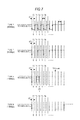
- the third determination method as described above, all communication systems of Type A, Type B, Type F at 212 kbps, and Type F at 424 kbps can be determined, and an example of the method will be explained according to FIG. 7 .
- the communication system determination circuit 13 detects a trailing edge of the binarized signal supplied from the demodulation circuit 12 .
- the demodulation circuit 12 detects the trailing edge of the binarized signal
- the communication system determination circuit 13 receives the supply of the binarized signal from the demodulation circuit 12 and detects the trailing edge.
- the communication system determination circuit 13 sets a time after a lapse of t/2 time when the period of 16/fc is t from the time when the first trailing edge of the binarized signal is detected to a base time T 0 . Then, the communication system determination circuit 13 detects the signal level of the binarized signal at the predetermined number of times after a lapse of t time including the base time T 0 .
- how many times the level of the binarized signal is detected varies depending on the combination of communication systems to be determined. In other words, the number of times varies depending on the types of the communication systems in which the reader writer may transmit.
- results of detection of the signal levels of the binarized signals of the respective communication systems will be explained regarding the five times of T 1 , T 2 , T 3 , T 4 at each time after a lapse of t time from the base time T 0 .
- the high (Hi) signal level is expressed by “1”, and the low (Low) signal level is expressed by “0”.
- the binarized signal has repeats rising and trailing edges at t time intervals (with a period of 16/fc) from the first trailing edge. Therefore, the signal levels of the binarized signal at the times T 0 , T 1 , T 2 , T 3 , T 4 are “0”, “1”, “0”, “1”, “0”, respectively.
- the binarized signal repeats rising and trailing edges at 2t time intervals (with a period of 32/fc) from the first trailing edge. Therefore, the signal levels of the binarized signal at the times T 0 , T 1 , T 2 , T 3 , T 4 are “0”, “0”, “1”, “1”, “0”, respectively.
- the binarized signal takes zero from the first trailing edge to at least 2 ⁇ sec and definitely takes one after 3 ⁇ sec from the first trailing edge to 9.4 ⁇ sec as shown in FIG. 2 .
- the value may change between 2 ⁇ sec and 3 ⁇ sec from the first trailing edge.
- the time T 1 is before a lapse of 2 ⁇ sec from the first trailing edge, and the time T 2 is between 2 ⁇ sec and 3 ⁇ sec from the first trailing edge. Therefore, the signal levels of the binarized signal at the times T 0 , T 1 , T 2 , T 3 , T 4 are “0”, “0”, “0” or “1”, “1”, “1”, respectively.
- the binarized signal takes zero from the first trailing edge to 94 ⁇ sec. Therefore, the signal levels of the binarized signal at the times T 0 , T 1 , T 2 , T 3 , T 4 are “0”, “0”, “0”, “0”, “0”, respectively.
- all communication systems of Type A, Type B, Type F at 212 kbps, and Type F at 424 kbps can be determined by detection of the five signal levels of the binarized signal at least at the times T 0 , T 1 , T 2 , T 3 , T 4 .
- the communication system determination circuit 13 determines the communication system as Type F at 424 kbps when the five signal levels of the binarized signal at the times T 0 , T 1 , T 2 , T 3 , T 4 are “0”, “1”, “0”, “1”, “0”, respectively.
- the communication system determination circuit 13 determines the communication system as Type F at 212 kbps when five signal levels of the binarized signal at the times T 0 , T 1 , T 2 , T 3 , T 4 are “0”, “0”, “1”, “1”, “0”, respectively.
- the communication system determination circuit 13 determines the communication system as Type A when five signal levels of the binarized signal at the times T 0 , T 1 , T 2 , T 3 , T 4 are “0”, “0”, “0” or “1”, “1”, “1”, respectively.
- the communication system determination circuit 13 determines the communication system as Type B when five signal levels of the binarized signal at the times T 0 , T 1 , T 2 , T 3 , T 4 are “0”, “0”, “0”, “0”, “0”, respectively.
- the communication system determination circuit 13 can determine the communication system based on the result of the signal levels of the binarized signal at the total of five times including the base time T 0 at each time after a lapse oft time from the base time T 0 .
- how many times the level of the binarized signal is determined varies depending on the combination of communication systems to be determined. For example, in the case where only three communication systems of Type F at 424 kbps, and Type F at 212 kbps, and Type B are determined, a total of four times of detection of signal levels of the binarized signal may be performed. The determination can be made, when the four signal levels of the binarized signal are “0”, “1”, “0”, “1”, as Type F at 424 kbps, when the four signal levels of the binarized signal are “0”, “0”, “1”, “1”, as Type F at 212 kbps, and, when the four signal levels of the binarized signal are “0”, “0”, “0”, “0”, as Type B.
- the period with which the signal levels are detected varies depending on the combination of communication systems to be determined.
- the period with which the signal levels are detected may be a period of 32/fc. That is, the period with which the signal levels are detected may be a half of 1 etu, which is the shortest among the communication systems to be determined, or less. Note that the number of times of detection can be made smallest when the period with which the signal levels are detected is set to a half of 1 etu, which is the shortest among the communication systems to be determined, and, when the period is made shorter, the number of times of detection of the signal levels of the binarized signal increases.
- the communication system determination circuit 13 includes a CPU, a ROM, etc., and the CPU executes a program stored in the memory unit 15 , and thereby, the circuit executes the above described third determination processing. Further, the period and the number of times of detection of signal levels can be stored as parameters in the memory unit 15 . Thereby, in the case where the communication systems to be determined are decided according to the application of the IC card 1 , the period and the number of times according to the communication system to be determined can easily be set. In this manner, various combinations of communication systems to be determined can flexibly be responded and determination in a short time according to the communication system to be determined can be performed.
- FIG. 8 is a flowchart for explanation of third determination processing. This processing is executed when the electromagnetic wave from the reader writer is received and supply of power to the respective units of the IC card 1 is started.
- the communication system determination circuit 13 reads out the program stored in the memory unit 15 and reads out and sets a period t stored as a parameter in the memory unit 15 at step S 41 .
- “16/fc” is stored as the period t in the memory unit 15 , and the communication system determination circuit 13 sets the period t to “16/fc”.
- the communication system determination circuit 13 reads out and sets a detection counter C stored as a parameter for deciding the number of times of detection of signal levels from the memory unit 15 .
- a detection counter C stored as a parameter for deciding the number of times of detection of signal levels from the memory unit 15 .
- “5” is stored as the detection counter C in the memory unit 15 , and the communication system determination circuit 13 sets the detection counter C to “5”.
- the communication system determination circuit 13 determines whether a trailing edge of the binarized signal has been detected or not, and waits until the determination that a trailing edge of the binarized signal has been detected is made.
- step S 43 If the determination that a trailing edge of the binarized signal has been detected is made at step S 43 , the process moves to step S 44 , and the communication system determination circuit 13 waits in t/2 time from the time when the trailing edge is detected.
- the t time in the embodiment is equal to a period of 16/fc.
- the communication system determination circuit 13 detects a signal level of the binarized signal as step S 45 .
- the detection of the signal level at step S 45 is detection at the base time T 0 .
- the communication system determination circuit 13 sets a new detection counter C to a value obtained by subtracting one from the detection counter C.
- step S 47 the communication system determination circuit 13 determines whether the detection counter C is zero or not. If the determination that the detection counter C is not zero is made at step S 47 , the process moves to step S 48 .
- step S 48 the communication system determination circuit 13 waits in t time and the process is returned to step S 45 after a lapse of t time.
- the processing at steps S 45 to 48 is repeated until the determination that the detection counter C is zero is made at step S 47 after the process is returned to step S 45 .
- the detected signal level when the detection counter C is “4” corresponds to the signal level at base time T 1
- the detected signal level when the detection counter C is “3” corresponds to the signal level at base time T 2
- the signal levels detected when the detection counter C is “2”, “1”, “0” correspond to the signal levels at base times T 2 , T 3 , T 4 , respectively.
- step S 47 the process moves to step S 49 , and the communication system determination circuit 13 determines whether the signal level of the second bit is “1” or not.
- step S 49 If the determination that signal level of the second bit is “1” is made at step S 49 , that is, if the signal level of the base time T 1 is “1”, the process proceeds to step S 50 where the communication system determination circuit 13 determines the communication system of the reader writer as Type F at 424 kbps.
- step S 49 the process proceeds to step S 51 where the communication system determination circuit 13 determines whether the signal level of the fourth bit is “0” or not.
- step S 51 determines whether signal level of the fourth bit is “0” is made at step S 51 , that is, if the signal level of the base time T 3 is “0”, the process proceeds to step S 52 where the communication system determination circuit 13 determines the communication system of the reader writer as Type B.
- step S 51 determines whether the signal level of the fourth bit is “0” or not.
- step S 53 If the determination that signal level of the fifth bit is “1” is made at step S 53 , that is, if the signal level of the base time T 4 is “1”, the process proceeds to step S 54 where the communication system determination circuit 13 determines the communication system of the reader writer as Type A.
- step S 53 determines the communication system of the reader writer as Type F at 212 kbps.
- step S 56 the communication system determination circuit 13 checks the format according to the determined communication system. This processing is the same as the processing at steps S 5 , S 6 , S 9 , S 10 , S 13 , and S 14 in FIG. 5 .
- the communication system determination circuit 13 confirms whether the preamble field, the Sync field, the length field, and the CRC field can be read out and contents of them are correct or not.
- the communication system determination circuit 13 confirms whether the parity, the end bit indicating the end of communication can be read out and contents of them are correct or not.
- the communication system determination circuit 13 confirms whether the SOF, EOF, CRC can be read out and contents of them are correct or not.
- the communication system determination circuit 13 supplies the read out data to the data processing unit 14 at step S 57 . Further, the communication system determination circuit 13 supplies data supplied from the data processing unit 14 as a response corresponding to the transmission from the reader writer to the modulation circuit 16 X or 16 Y corresponding to the determination result.
- the communication system can be determined according to the detection result when the signal levels of the binarized signal are detected with the predetermined period at the predetermined number of times.
- the communication system can be determined by the detection of the signal levels of the binarized signal with the period of 16/fc (t time) at five times. In this case, determination can be made within 5t time and the determination can be made faster than the determination after reception of the entire frame.
- the confirmation of the format is also performed, and therefore, even if the determination result of the communication system is erroneous, the error can be detected.
- the IC card 1 can repeatedly execute the third determination processing. Thereby, for example, if the error of the determination result is detected by the check of the format in the first execution, the correct communication system can be determined by the second or subsequent execution and communication with the reader writer can be started.
- the third determination processing is executed by software processing based on the programs and parameters stored in the memory unit 15 , and thereby, can flexibly respond various combinations of communication systems to be determined. Further, determination in a short time according to various combinations of communication systems to be determined can be performed.
- the IC card 1 As described above, according to the IC card 1 to which the embodiments of the invention are applied, plural communication systems can be supported and communication can be established in a short time for any communication system. Further, it is not necessary to provide reception circuits respectively corresponding to the plural communication systems, the simple configuration may be employed and the IC card 1 can be manufactured at low cost. That is, according to the IC card 1 , communication can be established with the simple configuration in a short time for the plural communication systems.
- the device that performs the first to third determination processing which has been explained as the IC card 1 in the above described examples, is not limited to the IC card, but may be an IC tag, a cellular phone, or the like other than the card type. That is, the communication device that performs noncontact communication by executing the first to third determination processing may be incorporated into an electronic device having other functions as a part thereof.
- the steps described in the flowcharts contain not only the processing that is time-sequentially performed in the described order but also the processing not necessarily time-sequentially performed but performed in parallel or individually.
Landscapes
- Engineering & Computer Science (AREA)
- Computer Networks & Wireless Communication (AREA)
- Signal Processing (AREA)
- Power Engineering (AREA)
- Physics & Mathematics (AREA)
- Spectroscopy & Molecular Physics (AREA)
- Near-Field Transmission Systems (AREA)
Applications Claiming Priority (2)
| Application Number | Priority Date | Filing Date | Title |
|---|---|---|---|
| JPP2009-074054 | 2009-03-25 | ||
| JP2009074054A JP5339138B2 (ja) | 2009-03-25 | 2009-03-25 | 通信装置、通信方法、およびプログラム |
Publications (2)
| Publication Number | Publication Date |
|---|---|
| US20100248624A1 US20100248624A1 (en) | 2010-09-30 |
| US8543056B2 true US8543056B2 (en) | 2013-09-24 |
Family
ID=42320389
Family Applications (1)
| Application Number | Title | Priority Date | Filing Date |
|---|---|---|---|
| US12/721,739 Expired - Fee Related US8543056B2 (en) | 2009-03-25 | 2010-03-11 | Communication device, communication method, and program |
Country Status (4)
| Country | Link |
|---|---|
| US (1) | US8543056B2 (enExample) |
| EP (1) | EP2234356A2 (enExample) |
| JP (1) | JP5339138B2 (enExample) |
| CN (1) | CN101848015A (enExample) |
Families Citing this family (12)
| Publication number | Priority date | Publication date | Assignee | Title |
|---|---|---|---|---|
| JP5323556B2 (ja) * | 2009-03-30 | 2013-10-23 | フェリカネットワークス株式会社 | 演算回路、信号選択方法及びコンピュータプログラム |
| KR101610916B1 (ko) * | 2010-02-23 | 2016-04-11 | 삼성전자주식회사 | 근거리 통신을 위한 수신 장치와 그에 따른 통신 모드 검출방법 |
| JP2014505285A (ja) * | 2010-12-03 | 2014-02-27 | グーグル・インコーポレーテッド | タップによる複数のデバイス間の対話および通信プロトコル |
| US9390414B2 (en) | 2011-09-18 | 2016-07-12 | Google Inc. | One-click offline buying |
| FR2980874B1 (fr) | 2011-09-30 | 2018-06-08 | Proton World International N.V. | Configuration du type de modulation d'un routeur de communication en champ proche |
| FR2980873B1 (fr) | 2011-09-30 | 2015-08-07 | Proton World Int Nv | Configuration d'un routeur de communication en champ proche en type de modulation |
| CN102522998A (zh) * | 2011-11-12 | 2012-06-27 | 广州中大微电子有限公司 | 一种适用于nrz编码信号的typeb全速率解码电路 |
| CN102663456B (zh) * | 2012-02-01 | 2015-09-16 | 深圳市华士精成科技有限公司 | 一种近距离有源射频识别系统 |
| JP2014235595A (ja) * | 2013-06-03 | 2014-12-15 | 株式会社リコー | 非接触型通信方式判定回路、非接触型通信回路及びicカード |
| FR3065349B1 (fr) * | 2017-04-12 | 2019-05-03 | Safran Electronics & Defense | Systeme comportant une baie et un module remplacable en ligne |
| JP7215227B2 (ja) * | 2019-02-28 | 2023-01-31 | 富士通株式会社 | 無線信号復調装置、無線信号復調プログラム、及び無線信号復調方法 |
| WO2022173857A1 (en) * | 2021-02-11 | 2022-08-18 | National Currency Technologies, Inc. | Centralized tracking for digital currencies |
Citations (10)
| Publication number | Priority date | Publication date | Assignee | Title |
|---|---|---|---|---|
| US6157024A (en) * | 1999-06-03 | 2000-12-05 | Prospects, Corp. | Method and apparatus for improving the performance of an aperture monitoring system |
| JP2003233787A (ja) | 2002-02-08 | 2003-08-22 | Nippon Telegr & Teleph Corp <Ntt> | 非接触icカード交信確立方法及びシステム装置 |
| US20040213169A1 (en) * | 2001-10-23 | 2004-10-28 | Inside Contactless | Contact-free integrated circuit having automatic frame identification means |
| JP2005339141A (ja) | 2004-05-26 | 2005-12-08 | Dainippon Printing Co Ltd | 携帯型情報記憶媒体、情報処理装置、プログラム及び通信確立方法 |
| US20060038024A1 (en) * | 2004-08-18 | 2006-02-23 | Renesas Technology Corp. | Semiconductor integrated circuit device and noncontact IC card |
| WO2006110000A1 (en) * | 2005-04-15 | 2006-10-19 | Ktfreetel Co., Ltd. | Contactless type integrated circuit card and method for communicating data by multiprotocol |
| JP2008059271A (ja) | 2006-08-31 | 2008-03-13 | Toshiba Corp | 情報通信媒体 |
| US20090132898A1 (en) * | 2007-11-19 | 2009-05-21 | Felica Networks, Inc. | Ic card, information processing device, communication type identification method, and program |
| US20090177954A1 (en) * | 2006-06-20 | 2009-07-09 | Kazuaki Takahashi | Code error detecting device, wireless system and code error detecting method |
| US20100124258A1 (en) * | 2008-11-20 | 2010-05-20 | Renesas Technology Corp. | Semiconductor device and communication device |
Family Cites Families (6)
| Publication number | Priority date | Publication date | Assignee | Title |
|---|---|---|---|---|
| JP2000172806A (ja) * | 1998-12-08 | 2000-06-23 | Hitachi Ltd | 非接触icカード |
| JP4824195B2 (ja) * | 2001-05-18 | 2011-11-30 | 日本信号株式会社 | 非接触型icカード用リーダライタ及びその制御方法 |
| KR100560770B1 (ko) * | 2003-09-15 | 2006-03-13 | 삼성전자주식회사 | 실시간 프로토콜 전환 기능을 갖는 비접촉 집적회로 카드및 그것을 포함한 카드 시스템 |
| JP4576935B2 (ja) * | 2004-09-02 | 2010-11-10 | 株式会社日立製作所 | 非接触電子装置 |
| CN100573563C (zh) * | 2006-05-16 | 2009-12-23 | 张敏 | 一种非接触ic卡通用编码解码及读写装置和方法 |
| KR100935168B1 (ko) | 2007-09-21 | 2010-01-06 | 삼성전기주식회사 | 비수계 전도성 나노잉크 조성물 |
-
2009
- 2009-03-25 JP JP2009074054A patent/JP5339138B2/ja not_active Expired - Fee Related
-
2010
- 2010-03-09 EP EP10002427A patent/EP2234356A2/en not_active Withdrawn
- 2010-03-11 US US12/721,739 patent/US8543056B2/en not_active Expired - Fee Related
- 2010-03-17 CN CN201010143446A patent/CN101848015A/zh active Pending
Patent Citations (11)
| Publication number | Priority date | Publication date | Assignee | Title |
|---|---|---|---|---|
| US6157024A (en) * | 1999-06-03 | 2000-12-05 | Prospects, Corp. | Method and apparatus for improving the performance of an aperture monitoring system |
| US20040213169A1 (en) * | 2001-10-23 | 2004-10-28 | Inside Contactless | Contact-free integrated circuit having automatic frame identification means |
| JP2003233787A (ja) | 2002-02-08 | 2003-08-22 | Nippon Telegr & Teleph Corp <Ntt> | 非接触icカード交信確立方法及びシステム装置 |
| JP2005339141A (ja) | 2004-05-26 | 2005-12-08 | Dainippon Printing Co Ltd | 携帯型情報記憶媒体、情報処理装置、プログラム及び通信確立方法 |
| US20060038024A1 (en) * | 2004-08-18 | 2006-02-23 | Renesas Technology Corp. | Semiconductor integrated circuit device and noncontact IC card |
| JP2006060363A (ja) | 2004-08-18 | 2006-03-02 | Renesas Technology Corp | 半導体集積回路及び非接触icカード |
| WO2006110000A1 (en) * | 2005-04-15 | 2006-10-19 | Ktfreetel Co., Ltd. | Contactless type integrated circuit card and method for communicating data by multiprotocol |
| US20090177954A1 (en) * | 2006-06-20 | 2009-07-09 | Kazuaki Takahashi | Code error detecting device, wireless system and code error detecting method |
| JP2008059271A (ja) | 2006-08-31 | 2008-03-13 | Toshiba Corp | 情報通信媒体 |
| US20090132898A1 (en) * | 2007-11-19 | 2009-05-21 | Felica Networks, Inc. | Ic card, information processing device, communication type identification method, and program |
| US20100124258A1 (en) * | 2008-11-20 | 2010-05-20 | Renesas Technology Corp. | Semiconductor device and communication device |
Non-Patent Citations (1)
| Title |
|---|
| SN5472, SN7472 and-Gated J-K Master-Slave Flip-Flops With Preset and Clear, 1988, Texas Instruments, Dallas, TX; located at http://www.ti.com/lit/ds/symlink/sn5472.pdf. * |
Also Published As
| Publication number | Publication date |
|---|---|
| JP5339138B2 (ja) | 2013-11-13 |
| EP2234356A2 (en) | 2010-09-29 |
| CN101848015A (zh) | 2010-09-29 |
| US20100248624A1 (en) | 2010-09-30 |
| JP2010225069A (ja) | 2010-10-07 |
Similar Documents
| Publication | Publication Date | Title |
|---|---|---|
| US8543056B2 (en) | Communication device, communication method, and program | |
| US8422596B2 (en) | Communication device, communication method, and program | |
| US8643470B2 (en) | Semiconductor integrated circuit, IC card mounted with the semiconductor integrated circuit, and operation method for the same | |
| JP4239988B2 (ja) | 通信システム、通信装置、有線通信装置、および通信方法 | |
| US8537907B2 (en) | Receiving system for use in near field communication and mode detection method therefore | |
| US8250451B2 (en) | IC card, information processing device, communication type identification method, and program | |
| CN105453449B (zh) | 非接触式通信方法确定电路、非接触式通信电路、以及ic卡 | |
| JP4709895B2 (ja) | 多重プロトコルによるデータ通信のための非接触式icカード及びその通信方法 | |
| JP4206109B2 (ja) | 無線タグ読取り装置 | |
| EP1901201B1 (en) | RFID tag reader | |
| JP5428364B2 (ja) | 非接触型通信装置、その復号部 | |
| JP2009086984A (ja) | 非接触通信媒体読み取り装置、および非接触通信媒体読み取り方法 | |
| US10931331B2 (en) | Communication device and method | |
| CN101512545A (zh) | 无线数据传输系统中基站与至少一个应答器之间的编码数据传输方法 | |
| US20080292024A1 (en) | Amplitude-shift-keying (ask) radio-frequency (rf) signal decoding device and method thereof | |
| JP2010198396A (ja) | 無線タグリーダライタ及びその通信方法 | |
| JP2009271775A (ja) | 受信装置 | |
| JP2010136198A (ja) | 通信装置及び通信方法、同期装置及び同期方法、コンピューター・プログラム | |
| JP4412163B2 (ja) | 非接触型icカードリーダライタシステムおよびリーダライタ | |
| JP2008289197A (ja) | 無線タグ読取り装置 | |
| JP2008035104A (ja) | 通信装置及び信号処理方法 | |
| JP2005520379A (ja) | トランスポンダと通信するための通信局、および異なる伝送パラメータを用いた更なる通信局 | |
| Elrharbi et al. | RFID Communication Modes |
Legal Events
| Date | Code | Title | Description |
|---|---|---|---|
| AS | Assignment |
Owner name: SONY CORPORATION, JAPAN Free format text: ASSIGNMENT OF ASSIGNORS INTEREST;ASSIGNOR:MIYAKAWA, KEIICHIRO;REEL/FRAME:031053/0370 Effective date: 20100307 |
|
| FEPP | Fee payment procedure |
Free format text: PAYOR NUMBER ASSIGNED (ORIGINAL EVENT CODE: ASPN); ENTITY STATUS OF PATENT OWNER: LARGE ENTITY |
|
| REMI | Maintenance fee reminder mailed | ||
| LAPS | Lapse for failure to pay maintenance fees |
Free format text: PATENT EXPIRED FOR FAILURE TO PAY MAINTENANCE FEES (ORIGINAL EVENT CODE: EXP.) |
|
| STCH | Information on status: patent discontinuation |
Free format text: PATENT EXPIRED DUE TO NONPAYMENT OF MAINTENANCE FEES UNDER 37 CFR 1.362 |
|
| FP | Lapsed due to failure to pay maintenance fee |
Effective date: 20170924 |