US8525822B2 - LCD panel driving circuit having transition slope adjusting means and associated control method - Google Patents

LCD panel driving circuit having transition slope adjusting means and associated control method Download PDF

Info

Publication number
US8525822B2
US8525822B2 US12/769,901 US76990110A US8525822B2 US 8525822 B2 US8525822 B2 US 8525822B2 US 76990110 A US76990110 A US 76990110A US 8525822 B2 US8525822 B2 US 8525822B2
Authority
US
United States
Prior art keywords
driving signal
compliance
level
gate driving
lcd panel
Prior art date
Legal status (The legal status is an assumption and is not a legal conclusion. Google has not performed a legal analysis and makes no representation as to the accuracy of the status listed.)
Active, expires
Application number
US12/769,901
Other versions
US20100277458A1 (en
Inventor
Chi Kang Liu
Chin-Wei Lin
Min-Nan Hsieh
Current Assignee (The listed assignees may be inaccurate. Google has not performed a legal analysis and makes no representation or warranty as to the accuracy of the list.)
MediaTek Inc
Original Assignee
MStar Semiconductor Inc Taiwan
Priority date (The priority date is an assumption and is not a legal conclusion. Google has not performed a legal analysis and makes no representation as to the accuracy of the date listed.)
Filing date
Publication date
Application filed by MStar Semiconductor Inc Taiwan filed Critical MStar Semiconductor Inc Taiwan
Assigned to MSTAR SEMICONDUCTOR, INC. reassignment MSTAR SEMICONDUCTOR, INC. ASSIGNMENT OF ASSIGNORS INTEREST (SEE DOCUMENT FOR DETAILS). Assignors: LIU, CHI KANG, HSIEH, MIN-NAN, LIN, CHIN-WEI
Publication of US20100277458A1 publication Critical patent/US20100277458A1/en
Application granted granted Critical
Publication of US8525822B2 publication Critical patent/US8525822B2/en
Assigned to MEDIATEK INC. reassignment MEDIATEK INC. MERGER (SEE DOCUMENT FOR DETAILS). Assignors: MSTAR SEMICONDUCTOR, INC.
Active legal-status Critical Current
Adjusted expiration legal-status Critical

Links

Images

Classifications

    • GPHYSICS
    • G09EDUCATION; CRYPTOGRAPHY; DISPLAY; ADVERTISING; SEALS
    • G09GARRANGEMENTS OR CIRCUITS FOR CONTROL OF INDICATING DEVICES USING STATIC MEANS TO PRESENT VARIABLE INFORMATION
    • G09G3/00Control arrangements or circuits, of interest only in connection with visual indicators other than cathode-ray tubes
    • G09G3/20Control arrangements or circuits, of interest only in connection with visual indicators other than cathode-ray tubes for presentation of an assembly of a number of characters, e.g. a page, by composing the assembly by combination of individual elements arranged in a matrix no fixed position being assigned to or needed to be assigned to the individual characters or partial characters
    • G09G3/34Control arrangements or circuits, of interest only in connection with visual indicators other than cathode-ray tubes for presentation of an assembly of a number of characters, e.g. a page, by composing the assembly by combination of individual elements arranged in a matrix no fixed position being assigned to or needed to be assigned to the individual characters or partial characters by control of light from an independent source
    • G09G3/36Control arrangements or circuits, of interest only in connection with visual indicators other than cathode-ray tubes for presentation of an assembly of a number of characters, e.g. a page, by composing the assembly by combination of individual elements arranged in a matrix no fixed position being assigned to or needed to be assigned to the individual characters or partial characters by control of light from an independent source using liquid crystals
    • G09G3/3611Control of matrices with row and column drivers
    • G09G3/3685Details of drivers for data electrodes
    • G09G3/3688Details of drivers for data electrodes suitable for active matrices only
    • GPHYSICS
    • G09EDUCATION; CRYPTOGRAPHY; DISPLAY; ADVERTISING; SEALS
    • G09GARRANGEMENTS OR CIRCUITS FOR CONTROL OF INDICATING DEVICES USING STATIC MEANS TO PRESENT VARIABLE INFORMATION
    • G09G2330/00Aspects of power supply; Aspects of display protection and defect management
    • G09G2330/06Handling electromagnetic interferences [EMI], covering emitted as well as received electromagnetic radiation

Definitions

  • the present invention relates to a driving circuit on a liquid crystal display (LCD) panel and associated control method, and more particularly, to a driving circuit with low swing voltage on an LCD panel.
  • LCD liquid crystal display
  • FIG. 1 shows a schematic diagram of a conventional LCD panel and a driving circuit thereof.
  • an LCD panel 10 is divided into a display area 12 and a non-display area 14 .
  • the display area 12 comprises a thin-film transistor (TFT) array
  • the non-display area 14 comprises a gate driver 20 , a master source driver 40 and a slave source driver 60 for controlling transistors of the TFT array.
  • TFT thin-film transistor
  • the gate driver 20 needs 480 lines connected to the TFT array to control each of the 480 rows, and therefore the gate driver 20 is also referred as a row driver.
  • the master source driver 40 and the slave source driver 60 are referred as column drivers. Take a TFT array controlled by red (R), green (G) and blue (B) colors as an example.
  • the master source driver 40 and the slave source driver 60 need 2400 (800*3) lines connected to the TFT array to control 800 columns. Hence, the master source driver 40 needs 1200 lines and the slave source driver 60 needs 1200 lines.
  • a display controller 82 on a circuit board 80 outside the LCD panel 10 outputs a first digital image signal and a second digital image signal to the master source driver 40 and the slave source driver 60 on the LCD panel 10 via two flexible print circuits (FPC) 42 and 44 , respectively.
  • the master source driver 40 generates a gate driver signal to the gate driver 20 according to the first digital image signal.
  • the first digital image signal and the second digital image signal outputted by the display controller 82 are of transistor-transistor logic (TTL) logic level or complementary metal-oxide semiconductor (CMOS) logic level. That is, the high level is 3.3 V and the low level is 0 V.
  • the gate driving signal outputted by the master source driver 40 is also of a TTL or CMOS logic level.
  • Cost and area of the FPCs 42 and 44 connected between the circuit board 80 and the LCD panel 10 are proportional to each other.
  • An object of the present invention is to provide a driving circuit on an LCD panel, with a signal transmitted between drivers of the LCD panel having a low swing voltage and slow transition speed.
  • the present invention provides an LCD panel connected to a display controller.
  • the LCD panel comprises a main source driver for receiving a digital image signal in compliance with a first electrical specification from the display controller and converting the digital image signal to a gate driving signal and a slave source driving signal in compliance with a second electrical specification, a gate driver for receiving the gate driving signal in compliance with the second electrical specification, and a slave source driver for receiving the slave source driving signal in compliance with the second electrical specification.
  • the main source driver, the slave source driver and the gate driver drive a TFT array on the LCD panel according to the digital image signal, the gate driving signal and the slave source driving signal.
  • the present invention further provides a method for transmitting an LCD driving signal with low electromagnetic interference (EMI).
  • the method comprises receiving a digital image signal in compliance with a first electrical specification; generating a gate driving signal and a slave source driving signal in compliance with a second electrical specification according to the digital image data; and driving a TFT array on the LCD panel according to the digital image signal, the gate driving signal and the slave source driving signal, respectively.
  • EMI electromagnetic interference
  • FIG. 1 is a schematic diagram of a LCD panel and a driving circuit thereof according to the prior art.
  • FIG. 2 is a schematic diagram of an LCD panel and a driving circuit thereof in accordance with an embodiment of the present invention.
  • FIG. 3 is a schematic diagram of an LCD panel and a driving circuit thereof in accordance with another embodiment of the present invention.
  • FIG. 4A is a schematic diagram of a conversion output unit in accordance with an embodiment of the present invention.
  • FIG. 4B is a schematic diagram of a conversion output unit in accordance with another embodiment of the present invention.
  • FIG. 5 is a schematic diagram of a conversion input unit in accordance with an embodiment of the present invention.
  • FIG. 6 is a flow chart of a method for transmitting an LCD driving signal with low EMI in accordance with an embodiment of the present invention.
  • FIG. 2 shows a schematic diagram of an LCD panel and a driving circuit thereof in accordance with an embodiment of the present invention.
  • An LCD panel 100 comprises a display area 112 and a non-display area 114 .
  • the display area 112 comprises a TFT array; and the non-display area 114 comprises a gate driver 120 , a main source driver 140 and a slave source driver 160 for driving transistors of the TFT array.
  • a display controller 182 on a circuit board 180 utilizes an FPC 150 to transmit a digital image signal to the main source driver 140 , which generates a slave source driving signal and a gate driving signal to the slave source driver 160 and the gate driver 120 , respectively.
  • the digital image signal, the gate driving signal and the slave source driving signal are of TTL or CMOS logic level. Since the cost and area of the FPC 150 are proportional to each other, the FPC 150 for transmitting the digital image signal reduces cost while improving signal quality. Detailed description on the FPC 150 is disclosed below.
  • a shielding metal covering traces between the slave source driving signal and the gate driving signal on the LCD panel is applied for reducing EMI.
  • the TTL or CMOS logic level signals i.e., the gate driving signal and the slave source driving signal, are converted to signals with a low swing voltage and slow transition speed, so as to reduce EMI without the shielding metal.
  • FIG. 3 shows a schematic diagram of an LCD panel and a driving circuit thereof in accordance with another embodiment of the present invention.
  • a master source driver 190 comprises a main circuit 192 and a conversion output unit 194 .
  • the main circuit 192 mainly operates in the identical way as the master source driver 140 illustrated in FIG. 2 .
  • the main circuit 192 receives the digital image signal outputted by the display controller 182 and outputs a slave source driving signal and a gate driving signal of TTL or CMOS logic level to the conversion output unit 194 .
  • the conversion output unit 194 receives and converts the slave source driving signal and the gate driving signal of TTL or CMOS logic level to signals with a low swing voltage and slow transition speed.
  • the gate driver 120 and the slave source driver 160 respectively comprising conversion input units 122 and 162 , convert the received signals with the low swing voltage and slow transition speed to a gate driving signal and a slave source driving signal of TTL or CMOS logic level. Therefore, signals transmitted on the LCD panel are the gate driving signal and the slave source driving signal with low swing voltages and slow transition speed. Therefore, according to this embodiment of the present invention, not only is shielding metal spared but EMI is also effectively reduced.
  • FIG. 4A shows a conversion output unit in accordance with an embodiment of the present invention.
  • the conversion output unit comprises a first PMOS transistor Mp 1 , a second PMOS transistor Mp 2 , a first NMOS transistor Mn 1 and a second NMOS transistor Mn 2 .
  • the first PMOS transistor Mp 1 has its source connected to a 3.3V voltage source, and its gate connected to its drain to form a diode connected transistor.
  • the second NMOS transistor Mn 2 has its source connected to ground, and its gate connected to its drain to form a diode connected transistor.
  • the second PMOS transistor Mp 2 and the first NMOS transistor Mn 1 form a buffer 196 .
  • the second PMOS transistor Mp 2 has its drain connected to the drain of the first PMOS transistor Mp 1
  • the first NMOS transistor Mn 1 has its gate connected to the gate of the second PMOS transistor Mp 2 to form an input end of a buffer 196 .
  • the second PMOS transistor Mp 2 has its drain connected to the drain of the first NMOS transistor Mn 1 to form an output end of the buffer 196
  • the first NMOS transistor Mn 1 has its source connected to the drain of the second NMOS transistor Mn 2 .
  • the first PMOS transistor Mp 1 and the second NMOS transistor Mn 2 are configured as diode connected transistors.
  • a drain voltage of the first PMOS transistor Mp 1 is V 1
  • a drain voltage of the second NMOS transistor Mn 2 is V 2 , where Vcc>V 1 >V 2 > 0 . Therefore, a conversion output unit illustrated in FIG. 4A reduces the voltage swing from 3.3V to a difference by subtracting V 2 from V 1 .
  • the conversion output unit comprises a first buffer 202 , a second buffer 204 , a third buffer 206 , a first delay unit 208 and a second delay unit 210 .
  • the first buffer 202 , the second buffer 204 and the third buffer 206 being identical to the buffer 196 illustrated in FIG. 4A , are connected to voltage sources V 1 and V 2 .
  • the first delay unit 208 and the second delay unit 210 have different delay time.
  • a signal input end is directly connected to an input end of the first buffer 202 .
  • the signal input end is connected to an input end of the first delay unit 208 , of which an output end is connected to an input end of the second buffer 204 .
  • the signal input end is also connected to an input end of the second delay unit 210 , of which an output end is connected to an input end of the third buffer 206 .
  • the conversion output unit illustrated in FIG. 4B further reduces a first transition slope to a second transition slope.
  • FIG. 5 shows a schematic diagram of a conversion input unit in accordance with an embodiment of the present invention.
  • the conversion input unit comprises a comparator 220 , a first resistor R 1 and a second resistor R 2 .
  • the first resistor R 1 and the second resistor R 2 are serially connected between a 3.3V voltage source and the ground to form a voltage dividing circuit for providing a threshold voltage Vth to a positive input end of the comparator 220 .
  • a signal input end is connected to a negative input end of the comparator 220 .
  • the conversion input unit in addition to increasing a voltage swing from V 1 -V 2 to 3.3V, the conversion input unit also increases a second transition slope to a first transition slope.
  • FIG. 6 shows a flow chart of a method for transmitting an LCD driving signal with low EMI in accordance with an embodiment of the present invention.
  • a master source driver receives a digital image signal via an FPC and converts the digital image signal to a gate driving signal and a slave source driving signal, which are compliant with another specification such as a High-Speed Transceiver Logic (HSTL) specification or a Stub Series Terminated Logic (SSTL) specification.
  • the digital image signal is compliant with a low voltage differential signal (LVDS) specification.
  • LVDS low voltage differential signal
  • the swing voltage and the transition speed of the gate driving signal and the slave source driving signal, compliant with the another specification is smaller than those of signals compliant with a TTL or CMOS logic specification.
  • a gate driver receives and converts the gate driving signal in compliance with the another specification to the gate driving signal in compliance with TTL or CMOS logic specification.
  • the gate driving signal in compliance with TTL or CMOS logic specification swings between a first level and a second level
  • the gate driving signal of the another specification swings between a third level and a fourth level.
  • the first level is greater than the third level
  • the third level is greater than the fourth level
  • the fourth level is greater than the second level.
  • the slave source driver receives and converts the slave source driving signal in compliance with the another specification to the slave source driving signal in compliance with TTL or CMOS logic specification.
  • the master source driver, the gate driver and the slave source driver drive a TFT array on an LCD panel with the gate driving signal and the slave source driving signal in compliance with the another specification, respectively.
  • the present invention provides a driving circuit on an LCD panel, with a signal transmitted on the LCD panel having a low swing voltage and adjustable slow high-low transition, such that EMI of the LCD panel is significantly reduced.

Abstract

A driving circuit on a liquid crystal display (LCD) panel and associated control method is provided. The LCD panel connected to a display control circuit via a flexible print circuit (FPC) includes a master source driver, for inputting a digital image signal in compliance with a first electrical specification via an FPC board and converting the digital image signal to a gate driving signal and a slave source driving signal, which are in compliance with a second electrical specification; a gate driver, for receiving the gate driving signal in compliance with the second electrical specification; and a slave source driver, for receiving the slave source driving signal in compliance with the second electrical specification. The master source driver, the slave source driver and the gate driver drive a thin-film transistor (TFT) on the LCD panel.

Description

CROSS REFERENCE TO RELATED PATENT APPLICATION
This patent application is based on Taiwan, R.O.C. patent application No. 098114456 filed on Apr. 30, 2009.
FIELD OF THE INVENTION
The present invention relates to a driving circuit on a liquid crystal display (LCD) panel and associated control method, and more particularly, to a driving circuit with low swing voltage on an LCD panel.
BACKGROUND OF THE INVENTION
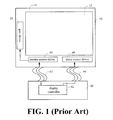
FIG. 1 shows a schematic diagram of a conventional LCD panel and a driving circuit thereof. Generally, an LCD panel 10 is divided into a display area 12 and a non-display area 14. The display area 12 comprises a thin-film transistor (TFT) array, and the non-display area 14 comprises a gate driver 20, a master source driver 40 and a slave source driver 60 for controlling transistors of the TFT array.
Taking an LCD panel with a resolution of 800*480 as an example, the gate driver 20 needs 480 lines connected to the TFT array to control each of the 480 rows, and therefore the gate driver 20 is also referred as a row driver. The master source driver 40 and the slave source driver 60 are referred as column drivers. Take a TFT array controlled by red (R), green (G) and blue (B) colors as an example. The master source driver 40 and the slave source driver 60 need 2400 (800*3) lines connected to the TFT array to control 800 columns. Hence, the master source driver 40 needs 1200 lines and the slave source driver 60 needs 1200 lines.
Conventionally, a display controller 82 on a circuit board 80 outside the LCD panel 10 outputs a first digital image signal and a second digital image signal to the master source driver 40 and the slave source driver 60 on the LCD panel 10 via two flexible print circuits (FPC) 42 and 44, respectively. The master source driver 40 generates a gate driver signal to the gate driver 20 according to the first digital image signal.
The first digital image signal and the second digital image signal outputted by the display controller 82 are of transistor-transistor logic (TTL) logic level or complementary metal-oxide semiconductor (CMOS) logic level. That is, the high level is 3.3 V and the low level is 0 V. Similarly, the gate driving signal outputted by the master source driver 40 is also of a TTL or CMOS logic level.
Cost and area of the FPCs 42 and 44 connected between the circuit board 80 and the LCD panel 10 are proportional to each other.
SUMMARY OF THE INVENTION
An object of the present invention is to provide a driving circuit on an LCD panel, with a signal transmitted between drivers of the LCD panel having a low swing voltage and slow transition speed.
The present invention provides an LCD panel connected to a display controller. The LCD panel comprises a main source driver for receiving a digital image signal in compliance with a first electrical specification from the display controller and converting the digital image signal to a gate driving signal and a slave source driving signal in compliance with a second electrical specification, a gate driver for receiving the gate driving signal in compliance with the second electrical specification, and a slave source driver for receiving the slave source driving signal in compliance with the second electrical specification. The main source driver, the slave source driver and the gate driver drive a TFT array on the LCD panel according to the digital image signal, the gate driving signal and the slave source driving signal.
The present invention further provides a method for transmitting an LCD driving signal with low electromagnetic interference (EMI). The method comprises receiving a digital image signal in compliance with a first electrical specification; generating a gate driving signal and a slave source driving signal in compliance with a second electrical specification according to the digital image data; and driving a TFT array on the LCD panel according to the digital image signal, the gate driving signal and the slave source driving signal, respectively.
The advantages and spirit of the present invention can be further understood with the following detailed description and drawings. However, the present invention is not limited to the following description and drawings.
BRIEF DESCRIPTION OF THE DRAWINGS
FIG. 1 is a schematic diagram of a LCD panel and a driving circuit thereof according to the prior art.
FIG. 2 is a schematic diagram of an LCD panel and a driving circuit thereof in accordance with an embodiment of the present invention.
FIG. 3 is a schematic diagram of an LCD panel and a driving circuit thereof in accordance with another embodiment of the present invention.
FIG. 4A is a schematic diagram of a conversion output unit in accordance with an embodiment of the present invention.
FIG. 4B is a schematic diagram of a conversion output unit in accordance with another embodiment of the present invention.
FIG. 5 is a schematic diagram of a conversion input unit in accordance with an embodiment of the present invention.
FIG. 6 is a flow chart of a method for transmitting an LCD driving signal with low EMI in accordance with an embodiment of the present invention.
DETAILED DESCRIPTION OF THE PREFERRED EMBODIMENT
FIG. 2 shows a schematic diagram of an LCD panel and a driving circuit thereof in accordance with an embodiment of the present invention. An LCD panel 100 comprises a display area 112 and a non-display area 114. The display area 112 comprises a TFT array; and the non-display area 114 comprises a gate driver 120, a main source driver 140 and a slave source driver 160 for driving transistors of the TFT array.
A display controller 182 on a circuit board 180 utilizes an FPC 150 to transmit a digital image signal to the main source driver 140, which generates a slave source driving signal and a gate driving signal to the slave source driver 160 and the gate driver 120, respectively. The digital image signal, the gate driving signal and the slave source driving signal are of TTL or CMOS logic level. Since the cost and area of the FPC 150 are proportional to each other, the FPC 150 for transmitting the digital image signal reduces cost while improving signal quality. Detailed description on the FPC 150 is disclosed below.
Since the gate driving signal and the slave source driving signal are of TTL or CMOS logic level with frequencies about tens of MHz, a fast high-low transition may cause serious EMI. In order to solve the foregoing problem, a shielding metal covering traces between the slave source driving signal and the gate driving signal on the LCD panel is applied for reducing EMI.
Preferably, the TTL or CMOS logic level signals, i.e., the gate driving signal and the slave source driving signal, are converted to signals with a low swing voltage and slow transition speed, so as to reduce EMI without the shielding metal.
FIG. 3 shows a schematic diagram of an LCD panel and a driving circuit thereof in accordance with another embodiment of the present invention. A master source driver 190 comprises a main circuit 192 and a conversion output unit 194. The main circuit 192 mainly operates in the identical way as the master source driver 140 illustrated in FIG. 2. The main circuit 192 receives the digital image signal outputted by the display controller 182 and outputs a slave source driving signal and a gate driving signal of TTL or CMOS logic level to the conversion output unit 194.
The conversion output unit 194 receives and converts the slave source driving signal and the gate driving signal of TTL or CMOS logic level to signals with a low swing voltage and slow transition speed. The gate driver 120 and the slave source driver 160, respectively comprising conversion input units 122 and 162, convert the received signals with the low swing voltage and slow transition speed to a gate driving signal and a slave source driving signal of TTL or CMOS logic level. Therefore, signals transmitted on the LCD panel are the gate driving signal and the slave source driving signal with low swing voltages and slow transition speed. Therefore, according to this embodiment of the present invention, not only is shielding metal spared but EMI is also effectively reduced.
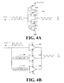
FIG. 4A shows a conversion output unit in accordance with an embodiment of the present invention. The conversion output unit comprises a first PMOS transistor Mp1, a second PMOS transistor Mp2, a first NMOS transistor Mn1 and a second NMOS transistor Mn2. For example, the first PMOS transistor Mp1 has its source connected to a 3.3V voltage source, and its gate connected to its drain to form a diode connected transistor. The second NMOS transistor Mn2 has its source connected to ground, and its gate connected to its drain to form a diode connected transistor.
The second PMOS transistor Mp2 and the first NMOS transistor Mn1 form a buffer 196. The second PMOS transistor Mp2 has its drain connected to the drain of the first PMOS transistor Mp1, and the first NMOS transistor Mn1 has its gate connected to the gate of the second PMOS transistor Mp2 to form an input end of a buffer 196. The second PMOS transistor Mp2 has its drain connected to the drain of the first NMOS transistor Mn1 to form an output end of the buffer 196, and the first NMOS transistor Mn1 has its source connected to the drain of the second NMOS transistor Mn2.
Referring to FIG. 4A, the first PMOS transistor Mp1 and the second NMOS transistor Mn2 are configured as diode connected transistors. Suppose that a drain voltage of the first PMOS transistor Mp1 is V1 and a drain voltage of the second NMOS transistor Mn2 is V2, where Vcc>V1>V2>0. Therefore, a conversion output unit illustrated in FIG. 4A reduces the voltage swing from 3.3V to a difference by subtracting V2 from V1.
Referring to FIG. 4B showing a schematic diagram of a conversion output unit in accordance with another embodiment of the present invention. The conversion output unit comprises a first buffer 202, a second buffer 204, a third buffer 206, a first delay unit 208 and a second delay unit 210. The first buffer 202, the second buffer 204 and the third buffer 206, being identical to the buffer 196 illustrated in FIG. 4A, are connected to voltage sources V1 and V2. The first delay unit 208 and the second delay unit 210 have different delay time.
A signal input end is directly connected to an input end of the first buffer 202. The signal input end is connected to an input end of the first delay unit 208, of which an output end is connected to an input end of the second buffer 204. The signal input end is also connected to an input end of the second delay unit 210, of which an output end is connected to an input end of the third buffer 206.
In this embodiment, in addition to reducing a swing voltage from 3.3V to V1-V2, the conversion output unit illustrated in FIG. 4B further reduces a first transition slope to a second transition slope.
FIG. 5 shows a schematic diagram of a conversion input unit in accordance with an embodiment of the present invention. The conversion input unit comprises a comparator 220, a first resistor R1 and a second resistor R2. The first resistor R1 and the second resistor R2 are serially connected between a 3.3V voltage source and the ground to form a voltage dividing circuit for providing a threshold voltage Vth to a positive input end of the comparator 220. A signal input end is connected to a negative input end of the comparator 220. In this embodiment, in addition to increasing a voltage swing from V1-V2 to 3.3V, the conversion input unit also increases a second transition slope to a first transition slope.
FIG. 6 shows a flow chart of a method for transmitting an LCD driving signal with low EMI in accordance with an embodiment of the present invention. In Step 610, a master source driver receives a digital image signal via an FPC and converts the digital image signal to a gate driving signal and a slave source driving signal, which are compliant with another specification such as a High-Speed Transceiver Logic (HSTL) specification or a Stub Series Terminated Logic (SSTL) specification. For example, the digital image signal is compliant with a low voltage differential signal (LVDS) specification. The swing voltage and the transition speed of the gate driving signal and the slave source driving signal, compliant with the another specification, is smaller than those of signals compliant with a TTL or CMOS logic specification. It should be noted that, the swing voltage and the transition speed of the gate driving signal and the slave source driving signal compliant with the another specification are adjustable. In Step 620, a gate driver receives and converts the gate driving signal in compliance with the another specification to the gate driving signal in compliance with TTL or CMOS logic specification. The gate driving signal in compliance with TTL or CMOS logic specification swings between a first level and a second level, and the gate driving signal of the another specification swings between a third level and a fourth level. Preferably, the first level is greater than the third level, the third level is greater than the fourth level, and the fourth level is greater than the second level. In Step 630, the slave source driver receives and converts the slave source driving signal in compliance with the another specification to the slave source driving signal in compliance with TTL or CMOS logic specification. In Step 640, the master source driver, the gate driver and the slave source driver drive a TFT array on an LCD panel with the gate driving signal and the slave source driving signal in compliance with the another specification, respectively.
To sum up, the present invention provides a driving circuit on an LCD panel, with a signal transmitted on the LCD panel having a low swing voltage and adjustable slow high-low transition, such that EMI of the LCD panel is significantly reduced.
While the invention has been described in terms of what is presently considered to be the most practical and preferred embodiments, it is to be understood that the invention needs not to be limited to the above embodiments. On the contrary, it is intended to cover various modifications and similar arrangements included within the spirit and scope of the appended claims which are to be accorded with the broadest interpretation so as to encompass all such modifications and similar structures.

Claims (10)

What is claimed is:
1. A liquid crystal display (LCD) panel, coupled to a display controller, the LCD panel comprising:
a master source driver, for receiving a digital image signal in compliance with a first electrical specification from the display controller and converting the digital image signal to a gate driving signal and a slave source driving signal in compliance with a second electrical specification;
a gate driver, for receiving the gate driving signal in compliance with the second electrical specification; and
a slave source driver, for receiving the slave source driving signal in compliance with the second electrical specification,
wherein, the master source driver, the slave source driver and the gate driver drive a thin-film transistor (TFT) array on the LCD panel according to the digital image signal, the slave source driving signal and the gate driving signal, respectively,
wherein the master source driver comprises a main circuit and a conversion output unit, wherein the conversion output unit receives an output from the main circuit, and the conversion output unit comprises a plurality of buffers and at least one delay unit to adjust a transition slope of the output from the main circuit and produce the gate driving signal and the slave driving signal,
wherein the first electrical specification is a transistor-transistor logic (TTL) specification or a complementary metal-oxide-semiconductor (CMOS) logic specification,
wherein the main circuit is configured for receiving the digital image signal in compliance with the TTL specification or the CMOS logic specification and converting the digital image signal to another gate driving signal and another slave source driving signal in compliance with the TTL specification or the CMOS logic specification,
wherein the conversion output unit is configured for receiving said another gate driving signal and said another slave source driving signal in compliance with the TTL specification or the CMOS logic specification, and converting said another gate driving signal and said another slave source driving signal to the gate driving signal and the slave source driving signal in compliance with the second electrical specification,
wherein the conversion output unit comprises:
a first buffer;
a first delay unit;
a second buffer, with an input end connected to an output end of the first delay unit;
a second delay unit;
a third buffer, with an input end connected to an output end of the second delay unit; and
wherein the gate driving signal in compliance with the TTL specification or the CMOS logic specification is received at an input end of the first buffer, an input end of the first delay unit and an input end of the second delay unit, and the gate driving signal in compliance with the second electrical specification is outputted at an output end of the first buffer, the output end of the second buffer and the output end of the third buffer.
2. The LCD panel as claimed in claim 1, wherein a swing voltage and a transition speed of the gate driving signal and the slave source driving signal, in compliance with the second electrical specification, are smaller than those of signals in compliance with the TTL specification or the CMOS logic specifitcation.
3. The LCD panel as claimed in claim 1, wherein the second electronic specification is a High-Speed Transceiver Logic (HSTL) specification or a Stub Series Terminated Logic (SSTL) specification.
4. The LCD panel as claimed in claim 1, wherein the gate driver further comprises a conversion input unit for receiving and converting the gate driving signal in compliance with the second electric specification to another gate driving signal in compliance with the TTL specification or the CMOS logic specification.
5. The LCD panel as claimed in claim 1, wherein the plurality of buffers are configured for receiving and converting said another gate driving signal in compliance with the TTL specification or the CMOS logic specification to the gate driving signal in compliance with the second electrical specification; and
wherein the gate driving signal in compliance with the TTL specification or the CMOS logic specification swings between a first level and a second level, the gate driving signal in compliance with the second electrical specification swings between a third level and a fourth level, the first level is greater than the third level, the third level is greater than the fourth level, and the fourth level is greater than the second level.
6. The LCD panel as claimed in claim 1, wherein the gate driving signal in compliance with the TTL specification or the CMOS logic specification swings between a first level and a second level, the gate driving signal in compliance with the second electrical specification swings between a third level and a fourth level, the first level is greater than the third level, the third level is greater than the fourth level, and the fourth level is greater than the second level.
7. The LCD panel as claimed in claim 1, wherein the slave source driver comprises a conversion input unit for receiving and converting the slave source driving signal in compliance with the second electrical specification to another slave source driving signal in compliance with the TTL specification or the CMOS logic specification.
8. The LCD panel as claimed in claim 7, wherein the conversion input unit comprises:
a comparator, with a first end for receiving a reference voltage, a second end for receiving the slave source driving signal in compliance with the second electrical specification and an output end for outputting said another slave source driving signal in compliance with the TTL or the CMOS logic specification.
9. The LCD panel as claimed in claim 8, wherein said another slave source driving signal in compliance with the TTL specification or the CMOS logic specification swings between a first level and a second level, the slave source driving signal in compliance with the second electrical specification swings between a third level and a fourth level, the first level is greater than the third level, the third level is greater than the fourth level, and the fourth level is greater than the second level.
10. The LCD panel as claimed in claim 1, wherein the master source driver receives the digital image signal in compliance with the first electrical specification via a flexible printed circuit (FPC).
US12/769,901 2009-04-30 2010-04-29 LCD panel driving circuit having transition slope adjusting means and associated control method Active 2031-08-19 US8525822B2 (en)

Applications Claiming Priority (3)

Application Number Priority Date Filing Date Title
TW098114456 2009-04-30
TW098114456A TWI408659B (en) 2009-04-30 2009-04-30 Driving circuit on lcd panel and related control method
TW98114456A 2009-04-30

Publications (2)

Publication Number Publication Date
US20100277458A1 US20100277458A1 (en) 2010-11-04
US8525822B2 true US8525822B2 (en) 2013-09-03

Family

ID=43030039

Family Applications (1)

Application Number Title Priority Date Filing Date
US12/769,901 Active 2031-08-19 US8525822B2 (en) 2009-04-30 2010-04-29 LCD panel driving circuit having transition slope adjusting means and associated control method

Country Status (2)

Country Link
US (1) US8525822B2 (en)
TW (1) TWI408659B (en)

Cited By (4)

* Cited by examiner, † Cited by third party
Publication number Priority date Publication date Assignee Title
US20130009899A1 (en) * 2008-09-23 2013-01-10 Apple Inc. Display having a plurality of driver integrated circuits
US20160307544A1 (en) * 2015-04-17 2016-10-20 Sitronix Technology Corp. Display Apparatus and Computer System
US9647050B2 (en) 2014-06-03 2017-05-09 Samsung Display Co., Ltd. Flexible circuit film and display apparatus having the same
US20220224336A1 (en) * 2018-12-14 2022-07-14 Renesas Electronic America Inc. Digital logic compatible inputs in compound semiconductor circuits

Families Citing this family (8)

* Cited by examiner, † Cited by third party
Publication number Priority date Publication date Assignee Title
TWI441130B (en) * 2011-10-18 2014-06-11 Au Optronics Corp Intergrated source driving system and displayer comprising the same
CN103915068B (en) 2013-11-20 2016-04-20 上海中航光电子有限公司 A kind of liquid crystal indicator
CN105427828A (en) * 2016-01-08 2016-03-23 京东方科技集团股份有限公司 Display panel driving circuit, display panel driving method and display apparatus
JP6569743B2 (en) * 2016-01-19 2019-09-04 凸版印刷株式会社 Display device
US10706799B2 (en) * 2017-12-06 2020-07-07 Au Optronics Corporation Display device without a driver IC
TWI688938B (en) * 2018-05-22 2020-03-21 元太科技工業股份有限公司 Display device and display driving circuit with electromagnetic interference suppression capability
CN110517644B (en) * 2018-05-22 2021-01-26 元太科技工业股份有限公司 Display device capable of suppressing electromagnetic interference and display driving circuit
CN112530350B (en) * 2020-12-18 2023-07-18 厦门天马微电子有限公司 Display panel and display device

Citations (12)

* Cited by examiner, † Cited by third party
Publication number Priority date Publication date Assignee Title
US6211849B1 (en) * 1996-09-24 2001-04-03 Kabushiki Kaisha Toshiba Liquid crystal display device
US20020011999A1 (en) * 2000-07-27 2002-01-31 Kim Haeng-Seon Flat panel display
US20030112039A1 (en) * 2001-12-18 2003-06-19 Rankin Andrew M. 5 V Tolerant hot carrier injection (HCI) protection circuit
CN1584968A (en) 1999-11-05 2005-02-23 精工爱普生株式会社 Deriving device IC, electric optical appliance and electronic apparatus
US20050168429A1 (en) * 2004-02-03 2005-08-04 Chun-Yi Chou [flat panel display and source driver thereof]
US7075339B2 (en) * 2001-09-17 2006-07-11 Renesas Technology Corp. Semiconductor output circuit device
US20060187159A1 (en) * 2000-07-24 2006-08-24 Sharp Kabushiki Kaisha Display device and driver
US20070008009A1 (en) * 2005-07-01 2007-01-11 Samsung Electronics Co., Ltd. Source driver for controlling a slew rate and a method for controlling the slew rate
US20080094328A1 (en) * 1999-09-27 2008-04-24 Seiko Epson Corporation Electro-Optical Device, and Electronic Apparatus and Display Driver IC Using the Same
CN101340146A (en) 2008-08-26 2009-01-07 四川登巅微电子有限公司 Current summation conversion rate regulator delaying stage by stage
US20090274241A1 (en) * 2008-04-30 2009-11-05 Wen-Yuan Tsao Data Transmission Device and Related Method
US20100045587A1 (en) * 2008-08-19 2010-02-25 Au Optronics Corporation Driving apparatus for liquid crystal display

Family Cites Families (1)

* Cited by examiner, † Cited by third party
Publication number Priority date Publication date Assignee Title
KR100865329B1 (en) * 2007-03-29 2008-10-27 삼성전자주식회사 Display driver circuit, display device having the display driver circuit, and method for controlling signal thereof

Patent Citations (12)

* Cited by examiner, † Cited by third party
Publication number Priority date Publication date Assignee Title
US6211849B1 (en) * 1996-09-24 2001-04-03 Kabushiki Kaisha Toshiba Liquid crystal display device
US20080094328A1 (en) * 1999-09-27 2008-04-24 Seiko Epson Corporation Electro-Optical Device, and Electronic Apparatus and Display Driver IC Using the Same
CN1584968A (en) 1999-11-05 2005-02-23 精工爱普生株式会社 Deriving device IC, electric optical appliance and electronic apparatus
US20060187159A1 (en) * 2000-07-24 2006-08-24 Sharp Kabushiki Kaisha Display device and driver
US20020011999A1 (en) * 2000-07-27 2002-01-31 Kim Haeng-Seon Flat panel display
US7075339B2 (en) * 2001-09-17 2006-07-11 Renesas Technology Corp. Semiconductor output circuit device
US20030112039A1 (en) * 2001-12-18 2003-06-19 Rankin Andrew M. 5 V Tolerant hot carrier injection (HCI) protection circuit
US20050168429A1 (en) * 2004-02-03 2005-08-04 Chun-Yi Chou [flat panel display and source driver thereof]
US20070008009A1 (en) * 2005-07-01 2007-01-11 Samsung Electronics Co., Ltd. Source driver for controlling a slew rate and a method for controlling the slew rate
US20090274241A1 (en) * 2008-04-30 2009-11-05 Wen-Yuan Tsao Data Transmission Device and Related Method
US20100045587A1 (en) * 2008-08-19 2010-02-25 Au Optronics Corporation Driving apparatus for liquid crystal display
CN101340146A (en) 2008-08-26 2009-01-07 四川登巅微电子有限公司 Current summation conversion rate regulator delaying stage by stage

Cited By (10)

* Cited by examiner, † Cited by third party
Publication number Priority date Publication date Assignee Title
US20130009899A1 (en) * 2008-09-23 2013-01-10 Apple Inc. Display having a plurality of driver integrated circuits
US8743335B2 (en) * 2008-09-23 2014-06-03 Apple Inc. Display having a plurality of driver integrated circuits
US9647050B2 (en) 2014-06-03 2017-05-09 Samsung Display Co., Ltd. Flexible circuit film and display apparatus having the same
US10321568B2 (en) 2014-06-03 2019-06-11 Samsung Display Co., Ltd. Flexible circuit film having wires of different widths and display apparatus having the same
US10980118B2 (en) 2014-06-03 2021-04-13 Samsung Display Co., Ltd. Flexible circuit film including flexible films facing each other with wirings arranged there between
US11452207B2 (en) 2014-06-03 2022-09-20 Samsung Display Co., Ltd. Flexible circuit film and display apparatus having the same
US11653449B2 (en) 2014-06-03 2023-05-16 Samsung Display Co., Ltd. Flexible circuit film and display apparatus having the same
US20160307544A1 (en) * 2015-04-17 2016-10-20 Sitronix Technology Corp. Display Apparatus and Computer System
US9779697B2 (en) * 2015-04-17 2017-10-03 Sitronix Technology Corp. Display apparatus and computer system
US20220224336A1 (en) * 2018-12-14 2022-07-14 Renesas Electronic America Inc. Digital logic compatible inputs in compound semiconductor circuits

Also Published As

Publication number Publication date
US20100277458A1 (en) 2010-11-04
TWI408659B (en) 2013-09-11
TW201039331A (en) 2010-11-01

Similar Documents

Publication Publication Date Title
US8525822B2 (en) LCD panel driving circuit having transition slope adjusting means and associated control method
US8314763B2 (en) Display device transferring data signal with clock
KR102470761B1 (en) Buffer amplifier circuit for enhancing slew rate output signal thereof and decices having same
KR102396469B1 (en) Display device
CN100483194C (en) Liquid-crystal display and method of driving liquid-crystal display
US7609254B2 (en) Signal driving system for a display
KR100751441B1 (en) Flat panel display and source driver thereof
KR19990037514A (en) Interface circuit and liquid crystal drive circuit
US20180082653A1 (en) Display panel driving circuit, display panel driving method, and display device
CN109859684B (en) Display device and interface method thereof
US10748501B2 (en) Gate driver, display panel and display using same
KR102626066B1 (en) Level shifter and display device using the same
US10714046B2 (en) Display driver, electro-optical device, and electronic apparatus
JP2007116278A (en) Method for treating idle terminal and interface unit
JP5069389B2 (en) Flat panel display device
KR20130011173A (en) Interface driving circuit and flat display device inculding the same
US10417986B2 (en) Data driving system of liquid crystal display panel
US20180025696A1 (en) Display device and data driver
US11640780B2 (en) Data driver circuit correcting skew between a clock and data
KR20160036736A (en) Driving Circuit And Display Device Including The Same
KR102433746B1 (en) Gate drive integrated circuit and display device including the same
US7741871B2 (en) Integrated circuit device, electro-optical device, and electronic instrument
JP4434289B2 (en) Integrated circuit device, electro-optical device and electronic apparatus
CN101894526A (en) Driver on liquid crystal display panel and related control method
KR100989736B1 (en) Source driver and the liquid crystal display therewith

Legal Events

Date Code Title Description
AS Assignment

Owner name: MSTAR SEMICONDUCTOR, INC., TAIWAN

Free format text: ASSIGNMENT OF ASSIGNORS INTEREST;ASSIGNORS:LIU, CHI KANG;LIN, CHIN-WEI;HSIEH, MIN-NAN;SIGNING DATES FROM 20100408 TO 20100413;REEL/FRAME:024322/0648

STCF Information on status: patent grant

Free format text: PATENTED CASE

FPAY Fee payment

Year of fee payment: 4

AS Assignment

Owner name: MEDIATEK INC., TAIWAN

Free format text: MERGER;ASSIGNOR:MSTAR SEMICONDUCTOR, INC.;REEL/FRAME:052931/0468

Effective date: 20190115

MAFP Maintenance fee payment

Free format text: PAYMENT OF MAINTENANCE FEE, 8TH YEAR, LARGE ENTITY (ORIGINAL EVENT CODE: M1552); ENTITY STATUS OF PATENT OWNER: LARGE ENTITY

Year of fee payment: 8