US8430551B2 - Display apparatus and method of assembling the same - Google Patents
Display apparatus and method of assembling the same Download PDFInfo
- Publication number
- US8430551B2 US8430551B2 US13/193,273 US201113193273A US8430551B2 US 8430551 B2 US8430551 B2 US 8430551B2 US 201113193273 A US201113193273 A US 201113193273A US 8430551 B2 US8430551 B2 US 8430551B2
- Authority
- US
- United States
- Prior art keywords
- light
- guide plate
- light source
- backlight assembly
- light guide
- Prior art date
- Legal status (The legal status is an assumption and is not a legal conclusion. Google has not performed a legal analysis and makes no representation as to the accuracy of the status listed.)
- Active, expires
Links
Images


Classifications
-
- G—PHYSICS
- G02—OPTICS
- G02F—OPTICAL DEVICES OR ARRANGEMENTS FOR THE CONTROL OF LIGHT BY MODIFICATION OF THE OPTICAL PROPERTIES OF THE MEDIA OF THE ELEMENTS INVOLVED THEREIN; NON-LINEAR OPTICS; FREQUENCY-CHANGING OF LIGHT; OPTICAL LOGIC ELEMENTS; OPTICAL ANALOGUE/DIGITAL CONVERTERS
- G02F1/00—Devices or arrangements for the control of the intensity, colour, phase, polarisation or direction of light arriving from an independent light source, e.g. switching, gating or modulating; Non-linear optics
- G02F1/01—Devices or arrangements for the control of the intensity, colour, phase, polarisation or direction of light arriving from an independent light source, e.g. switching, gating or modulating; Non-linear optics for the control of the intensity, phase, polarisation or colour
- G02F1/13—Devices or arrangements for the control of the intensity, colour, phase, polarisation or direction of light arriving from an independent light source, e.g. switching, gating or modulating; Non-linear optics for the control of the intensity, phase, polarisation or colour based on liquid crystals, e.g. single liquid crystal display cells
- G02F1/133—Constructional arrangements; Operation of liquid crystal cells; Circuit arrangements
- G02F1/1333—Constructional arrangements; Manufacturing methods
- G02F1/1335—Structural association of cells with optical devices, e.g. polarisers or reflectors
- G02F1/1336—Illuminating devices
-
- G—PHYSICS
- G02—OPTICS
- G02B—OPTICAL ELEMENTS, SYSTEMS OR APPARATUS
- G02B6/00—Light guides; Structural details of arrangements comprising light guides and other optical elements, e.g. couplings
- G02B6/0001—Light guides; Structural details of arrangements comprising light guides and other optical elements, e.g. couplings specially adapted for lighting devices or systems
- G02B6/0011—Light guides; Structural details of arrangements comprising light guides and other optical elements, e.g. couplings specially adapted for lighting devices or systems the light guides being planar or of plate-like form
- G02B6/0081—Mechanical or electrical aspects of the light guide and light source in the lighting device peculiar to the adaptation to planar light guides, e.g. concerning packaging
-
- G—PHYSICS
- G02—OPTICS
- G02B—OPTICAL ELEMENTS, SYSTEMS OR APPARATUS
- G02B6/00—Light guides; Structural details of arrangements comprising light guides and other optical elements, e.g. couplings
- G02B6/0001—Light guides; Structural details of arrangements comprising light guides and other optical elements, e.g. couplings specially adapted for lighting devices or systems
- G02B6/0011—Light guides; Structural details of arrangements comprising light guides and other optical elements, e.g. couplings specially adapted for lighting devices or systems the light guides being planar or of plate-like form
- G02B6/0033—Means for improving the coupling-out of light from the light guide
- G02B6/005—Means for improving the coupling-out of light from the light guide provided by one optical element, or plurality thereof, placed on the light output side of the light guide
- G02B6/0053—Prismatic sheet or layer; Brightness enhancement element, sheet or layer
-
- G—PHYSICS
- G02—OPTICS
- G02B—OPTICAL ELEMENTS, SYSTEMS OR APPARATUS
- G02B6/00—Light guides; Structural details of arrangements comprising light guides and other optical elements, e.g. couplings
- G02B6/0001—Light guides; Structural details of arrangements comprising light guides and other optical elements, e.g. couplings specially adapted for lighting devices or systems
- G02B6/0011—Light guides; Structural details of arrangements comprising light guides and other optical elements, e.g. couplings specially adapted for lighting devices or systems the light guides being planar or of plate-like form
- G02B6/0033—Means for improving the coupling-out of light from the light guide
- G02B6/005—Means for improving the coupling-out of light from the light guide provided by one optical element, or plurality thereof, placed on the light output side of the light guide
- G02B6/0055—Reflecting element, sheet or layer
-
- G—PHYSICS
- G02—OPTICS
- G02B—OPTICAL ELEMENTS, SYSTEMS OR APPARATUS
- G02B6/00—Light guides; Structural details of arrangements comprising light guides and other optical elements, e.g. couplings
- G02B6/0001—Light guides; Structural details of arrangements comprising light guides and other optical elements, e.g. couplings specially adapted for lighting devices or systems
- G02B6/0011—Light guides; Structural details of arrangements comprising light guides and other optical elements, e.g. couplings specially adapted for lighting devices or systems the light guides being planar or of plate-like form
- G02B6/0065—Manufacturing aspects; Material aspects
-
- G—PHYSICS
- G02—OPTICS
- G02B—OPTICAL ELEMENTS, SYSTEMS OR APPARATUS
- G02B6/00—Light guides; Structural details of arrangements comprising light guides and other optical elements, e.g. couplings
- G02B6/0001—Light guides; Structural details of arrangements comprising light guides and other optical elements, e.g. couplings specially adapted for lighting devices or systems
- G02B6/0011—Light guides; Structural details of arrangements comprising light guides and other optical elements, e.g. couplings specially adapted for lighting devices or systems the light guides being planar or of plate-like form
- G02B6/0066—Light guides; Structural details of arrangements comprising light guides and other optical elements, e.g. couplings specially adapted for lighting devices or systems the light guides being planar or of plate-like form characterised by the light source being coupled to the light guide
- G02B6/0073—Light emitting diode [LED]
-
- G—PHYSICS
- G02—OPTICS
- G02B—OPTICAL ELEMENTS, SYSTEMS OR APPARATUS
- G02B6/00—Light guides; Structural details of arrangements comprising light guides and other optical elements, e.g. couplings
- G02B6/0001—Light guides; Structural details of arrangements comprising light guides and other optical elements, e.g. couplings specially adapted for lighting devices or systems
- G02B6/0011—Light guides; Structural details of arrangements comprising light guides and other optical elements, e.g. couplings specially adapted for lighting devices or systems the light guides being planar or of plate-like form
- G02B6/0081—Mechanical or electrical aspects of the light guide and light source in the lighting device peculiar to the adaptation to planar light guides, e.g. concerning packaging
- G02B6/0086—Positioning aspects
- G02B6/0088—Positioning aspects of the light guide or other optical sheets in the package
-
- G—PHYSICS
- G02—OPTICS
- G02B—OPTICAL ELEMENTS, SYSTEMS OR APPARATUS
- G02B6/00—Light guides; Structural details of arrangements comprising light guides and other optical elements, e.g. couplings
- G02B6/0001—Light guides; Structural details of arrangements comprising light guides and other optical elements, e.g. couplings specially adapted for lighting devices or systems
- G02B6/0011—Light guides; Structural details of arrangements comprising light guides and other optical elements, e.g. couplings specially adapted for lighting devices or systems the light guides being planar or of plate-like form
- G02B6/0081—Mechanical or electrical aspects of the light guide and light source in the lighting device peculiar to the adaptation to planar light guides, e.g. concerning packaging
- G02B6/0086—Positioning aspects
- G02B6/009—Positioning aspects of the light source in the package
-
- G—PHYSICS
- G02—OPTICS
- G02F—OPTICAL DEVICES OR ARRANGEMENTS FOR THE CONTROL OF LIGHT BY MODIFICATION OF THE OPTICAL PROPERTIES OF THE MEDIA OF THE ELEMENTS INVOLVED THEREIN; NON-LINEAR OPTICS; FREQUENCY-CHANGING OF LIGHT; OPTICAL LOGIC ELEMENTS; OPTICAL ANALOGUE/DIGITAL CONVERTERS
- G02F1/00—Devices or arrangements for the control of the intensity, colour, phase, polarisation or direction of light arriving from an independent light source, e.g. switching, gating or modulating; Non-linear optics
- G02F1/01—Devices or arrangements for the control of the intensity, colour, phase, polarisation or direction of light arriving from an independent light source, e.g. switching, gating or modulating; Non-linear optics for the control of the intensity, phase, polarisation or colour
- G02F1/13—Devices or arrangements for the control of the intensity, colour, phase, polarisation or direction of light arriving from an independent light source, e.g. switching, gating or modulating; Non-linear optics for the control of the intensity, phase, polarisation or colour based on liquid crystals, e.g. single liquid crystal display cells
- G02F1/133—Constructional arrangements; Operation of liquid crystal cells; Circuit arrangements
- G02F1/1333—Constructional arrangements; Manufacturing methods
- G02F1/1335—Structural association of cells with optical devices, e.g. polarisers or reflectors
- G02F1/133524—Light-guides, e.g. fibre-optic bundles, louvered or jalousie light-guides
-
- G—PHYSICS
- G02—OPTICS
- G02F—OPTICAL DEVICES OR ARRANGEMENTS FOR THE CONTROL OF LIGHT BY MODIFICATION OF THE OPTICAL PROPERTIES OF THE MEDIA OF THE ELEMENTS INVOLVED THEREIN; NON-LINEAR OPTICS; FREQUENCY-CHANGING OF LIGHT; OPTICAL LOGIC ELEMENTS; OPTICAL ANALOGUE/DIGITAL CONVERTERS
- G02F1/00—Devices or arrangements for the control of the intensity, colour, phase, polarisation or direction of light arriving from an independent light source, e.g. switching, gating or modulating; Non-linear optics
- G02F1/01—Devices or arrangements for the control of the intensity, colour, phase, polarisation or direction of light arriving from an independent light source, e.g. switching, gating or modulating; Non-linear optics for the control of the intensity, phase, polarisation or colour
- G02F1/13—Devices or arrangements for the control of the intensity, colour, phase, polarisation or direction of light arriving from an independent light source, e.g. switching, gating or modulating; Non-linear optics for the control of the intensity, phase, polarisation or colour based on liquid crystals, e.g. single liquid crystal display cells
- G02F1/133—Constructional arrangements; Operation of liquid crystal cells; Circuit arrangements
- G02F1/1333—Constructional arrangements; Manufacturing methods
- G02F1/1335—Structural association of cells with optical devices, e.g. polarisers or reflectors
- G02F1/1336—Illuminating devices
- G02F1/133615—Edge-illuminating devices, i.e. illuminating from the side
-
- G—PHYSICS
- G02—OPTICS
- G02B—OPTICAL ELEMENTS, SYSTEMS OR APPARATUS
- G02B6/00—Light guides; Structural details of arrangements comprising light guides and other optical elements, e.g. couplings
- G02B6/0001—Light guides; Structural details of arrangements comprising light guides and other optical elements, e.g. couplings specially adapted for lighting devices or systems
- G02B6/0011—Light guides; Structural details of arrangements comprising light guides and other optical elements, e.g. couplings specially adapted for lighting devices or systems the light guides being planar or of plate-like form
- G02B6/0013—Means for improving the coupling-in of light from the light source into the light guide
- G02B6/0015—Means for improving the coupling-in of light from the light source into the light guide provided on the surface of the light guide or in the bulk of it
- G02B6/0016—Grooves, prisms, gratings, scattering particles or rough surfaces
-
- G—PHYSICS
- G02—OPTICS
- G02B—OPTICAL ELEMENTS, SYSTEMS OR APPARATUS
- G02B6/00—Light guides; Structural details of arrangements comprising light guides and other optical elements, e.g. couplings
- G02B6/0001—Light guides; Structural details of arrangements comprising light guides and other optical elements, e.g. couplings specially adapted for lighting devices or systems
- G02B6/0011—Light guides; Structural details of arrangements comprising light guides and other optical elements, e.g. couplings specially adapted for lighting devices or systems the light guides being planar or of plate-like form
- G02B6/0013—Means for improving the coupling-in of light from the light source into the light guide
- G02B6/0015—Means for improving the coupling-in of light from the light source into the light guide provided on the surface of the light guide or in the bulk of it
- G02B6/002—Means for improving the coupling-in of light from the light source into the light guide provided on the surface of the light guide or in the bulk of it by shaping at least a portion of the light guide, e.g. with collimating, focussing or diverging surfaces
-
- Y—GENERAL TAGGING OF NEW TECHNOLOGICAL DEVELOPMENTS; GENERAL TAGGING OF CROSS-SECTIONAL TECHNOLOGIES SPANNING OVER SEVERAL SECTIONS OF THE IPC; TECHNICAL SUBJECTS COVERED BY FORMER USPC CROSS-REFERENCE ART COLLECTIONS [XRACs] AND DIGESTS
- Y10—TECHNICAL SUBJECTS COVERED BY FORMER USPC
- Y10T—TECHNICAL SUBJECTS COVERED BY FORMER US CLASSIFICATION
- Y10T29/00—Metal working
- Y10T29/49—Method of mechanical manufacture
- Y10T29/49002—Electrical device making
-
- Y—GENERAL TAGGING OF NEW TECHNOLOGICAL DEVELOPMENTS; GENERAL TAGGING OF CROSS-SECTIONAL TECHNOLOGIES SPANNING OVER SEVERAL SECTIONS OF THE IPC; TECHNICAL SUBJECTS COVERED BY FORMER USPC CROSS-REFERENCE ART COLLECTIONS [XRACs] AND DIGESTS
- Y10—TECHNICAL SUBJECTS COVERED BY FORMER USPC
- Y10T—TECHNICAL SUBJECTS COVERED BY FORMER US CLASSIFICATION
- Y10T29/00—Metal working
- Y10T29/49—Method of mechanical manufacture
- Y10T29/49826—Assembling or joining
Definitions
- the present disclosure is directed to a display apparatus and a method of assembling the same.
- the present disclosure is directed to a backlight unit of a display apparatus capable of improving display quality and reducing a number of parts and a method of assembling the backlight unit.
- Backlight assemblies having a light emitting diode have lower power consumption, higher brightness, and are slimmer, when compared to backlight assemblies having a cold cathode fluorescent lamp as its light source.
- the manufacturing cost of a backlight assembly increases for backlight assemblies using light emitting diodes as light sources instead of cold cathode fluorescent lamps.
- Exemplary embodiments of the present disclosure provide a display apparatus capable of reducing a number of parts.
- Exemplary embodiments of the present disclosure also provide a method of assembling the display apparatus.
- a backlight assembly of a display apparatus includes a light guide plate, a light source unit, and a receiving container.
- the light guide plate includes a chamfered corner portion that defines a light incident surface defined at the corner portion.
- the light source unit is disposed adjacent to the light incident surface to provide light to the light guide plate through the light incident surface.
- the receiving container includes sidewalls and a bottom portion extended from at least one of the sidewalls to accommodate the light guide plate and the light source unit.
- At least one of the sidewalls of the receiving container is divided into a first part and a second part at a position adjacent to the corner portion, and the first and second parts may be coupled to or separated from each other.
- a method of assembling the display apparatus is provided as follows.
- a light guide plate is prepared to have a chamfered corner portion to form a light incident surface positioned at the corner portion.
- a light source unit is disposed adjacent to the light incident surface to provide light to the light guide plate through the light incident surface.
- a receiving container including sidewalls and a bottom portion extending from at least one of the side walls is prepared.
- a sidewall disposed adjacent to the corner portion is divided into a first part and a second part. The second part may be separated from the first part to accommodate the light guide plate and the light source in the receiving container.
- the first and second parts may be coupled to each other after accommodating the light guide plate and the light source in the receiving container.
- a cover member is coupled to the receiving container to partially cover the display panel while exposing an area in which an image may be displayed.
- a backlight assembly includes a light guide plate, a light source unit, and a receiving container.
- the light guide plate includes a chamfered corner portion that forms a light incident surface at the corner portion.
- the light source unit is disposed adjacent to the light incident surface to provide light to the light guide plate through the light incident surface.
- the receiving container is configured to accommodate the light guide plate and the light source unit.
- a sidewall of the receiving container adjacent to the corner portion is divided into a first part and a second part configured to separate from each other to receive the light guide plate and light source unit.
- the light guide plate further includes an extended portion that extends from one side surface adjacent to the light incident surface, and lengthens the light incident surface.
- the sidewall adjacent to the light source unit is divided into the first part and the second part, and the first part may be coupled to the second part after accommodating the light guide plate and the light source unit in the receiving container.
- the light guide plate and the light source unit may be easily accommodated in the receiving container, improving assembling efficiency.
- FIG. 1 is a plan view showing a backlight assembly according to an exemplary embodiment of the present disclosure.
- FIG. 2 is a cross-sectional view taken along a line I-I′ of FIG. 1 .
- FIG. 3 is a partially enlarged view showing a portion A 1 of FIG. 1 .
- FIG. 4 is a perspective view partially showing a receiving container of FIG. 3 .
- FIG. 5 is a plan view showing first and second parts of the second sidewall, which are separated from each other.
- FIG. 6 is a plan view partially showing a backlight assembly according to another exemplary embodiment of the present disclosure.
- FIG. 7 is a cross-sectional view taken along a line II-II′ of FIG. 6 .
- FIG. 8 is a cross-sectional view showing a backlight assembly according to another exemplary embodiment of the present disclosure.
- FIG. 9 is a plan view partially showing a backlight assembly according to another exemplary embodiment of the present disclosure.
- FIG. 10 is a partially enlarged view showing a portion A 2 of FIG. 9 .
- FIG. 11 is a view showing a backside of the light guide plate of FIG. 1 .
- FIG. 12 is a plan view showing a display apparatus according to another exemplary embodiment of the present disclosure.
- FIG. 13 is a cross-sectional view taken along a line III-III′ of FIG. 12 .
- FIGS. 14A to 14C are views showing a light source unit of FIG. 12 in detail.
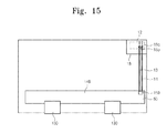
- FIG. 15 is a view showing a backside of the display apparatus of FIG. 12 .
- FIG. 16 is a plan view showing a connection part according to another exemplary embodiment of the present disclosure.
- FIG. 1 is a plan view showing a backlight assembly according to an exemplary embodiment of the present disclosure
- FIG. 2 is a cross-sectional view taken along a line I-I′ of FIG. 1 .
- a backlight assembly 100 includes a light guide plate 30 , a light source unit 10 , a receiving container 50 , a reflection plate 60 , and optical sheets 70 .
- the light guide plate 30 has a rectangular plate shape and receives light from the light source unit 10 to guide the light in a certain direction.
- the light guide plate 30 may guide the light received from the light source unit 10 to the liquid crystal display panel.
- the light guide plate 30 includes a chamfered corner portion that is provided with a light incident surface 32 defined by the chamfered corner portion.
- the light guide plate 30 includes a first side E 1 , a second side E 2 arranged adjacent to the first side E 1 , a third side E 3 facing the first side E 1 , and a fourth side E 4 facing the second side E 2 .
- the light incident surface 32 may be formed by chamfering the corner portion where the first side E 1 connects to the second side E 2 .
- the light guide plate 30 further includes an upper surface 31 connected to the first to fourth sides E 1 to E 4 that outputs the light and a lower surface 33 connected to the first to fourth sides E 1 to E 4 that is substantially parallel to the upper surface 31 .
- the light source unit 10 includes a light source 16 generating light, a back cover 18 covering the light source 16 , and a circuit board 12 on which the light source 16 is mounted to provide a driving power to the light source 16 .
- the light source 16 includes a light emitting surface 16 a facing and substantially parallel to the light incident surface 32 .
- the light source 16 may be a light emitting diode (LED), and the light source unit 10 may include a plurality of light emitting diodes.
- the back cover 18 is bent to surround the light source 16 and a portion of the back cover 18 is opened to expose the light emitting surface 16 a of the light source 16 .
- the back cover 18 may include a material, e.g., aluminum (Al), to reflect light exiting from the light source 16 to the light guide plate 30 , thereby increasing the light intensity provided to the light guide plate 30 .
- the circuit board 12 is electrically connected to the light source 16 and a power supply (not shown) and applies the driving power received from the power supply to the light source 16 .
- the circuit board 12 may be one of a flexible printed circuit (FPC) film, a double-sided flexible printed circuit film, or a metal printed circuit board (MPCB).
- the circuit board 12 may be disposed between the light source 16 and the back cover 18 .
- the receiving container 50 may include a first sidewall 51 , a second sidewall 52 , a third sidewall 53 , and a fourth sidewall 54 .
- the first sidewall 51 is arranged parallel to the first side E 1 of the light guide plate 30 to face the first side E 1 .
- the second sidewall 52 is arranged parallel to the second side E 2 of the light guide plate 30 to face the second side E 2 .
- the third sidewall 53 is arranged parallel to the third side E 3 of the light guide plate 30 to face the third side E 3 .
- the fourth 54 is arranged parallel to the fourth side E 4 of the light guide plate 30 to face the fourth side E 4 .
- the first to fourth sidewalls 51 , 51 , 53 , and 54 may form a rectangular frame shape. At least one of the first and second sidewalls 51 and 52 adjacent to the light incident surface 32 may be divided into two parts. In a present exemplary embodiment, the second sidewall 52 between the first and third sidewalls 51 and 53 is divided into a first part 56 and a second part 57 as shown in FIG. 1 . The second sidewall 52 may be divided into the first and second parts 56 and 57 in an area adjacent to the light incident surface 32 .
- the first and second parts 56 and 57 may have a structure in which end portions of the first and second parts 56 and 57 , which face each other, may couple to each other. More detailed descriptions of the structure of the first and second parts 56 and 57 will be described with reference to FIGS. 4 to 8 .
- the receiving container 50 may further include a cover part 58 that extends from the first, second, third, and fourth sidewalls 51 , 52 , 53 , and 54 to cover an edge portion of the upper surface 31 of the light guide plate 30 .
- the optical sheets 70 are mounted on the upper surface 31 of the light guide plate 30 .
- the optical sheets 70 may include at least one prism sheet condensing the light exiting from the light guide plate 30 to improve a front brightness and at least one diffusion sheet diffusing the light.
- End portions of the optical sheets 70 may be disposed between the cover part 58 and the light guide plate 30 .
- the cover part 58 may prevent the optical sheets 70 from separating from the light guide plate 30 .
- the backlight assembly 100 may further include the reflection plate 60 .
- the reflection plate 60 includes a material to reflect light, such as polyethylene terephthalate (PET) or aluminum, and is disposed between the bottom portion 55 of the receiving container 50 and the light guide plate 30 .
- PET polyethylene terephthalate
- the reflection plate 60 includes a material to reflect light, such as polyethylene terephthalate (PET) or aluminum, and is disposed between the bottom portion 55 of the receiving container 50 and the light guide plate 30 .
- PET polyethylene terephthalate
- the reflection plate 60 includes a material to reflect light, such as polyethylene terephthalate (PET) or aluminum, and is disposed between the bottom portion 55 of the receiving container 50 and the light guide plate 30 .
- PET polyethylene terephthalate
- the receiving container 50 is provided with a first user hole 51 a formed by removing a portion from the first sidewall 51 parallel to the first side E 1 and a second user hole 53 a formed by removing a portion from the third sidewall 53 parallel to the third side E 3 . More detailed description of the first and second user holes 51 a and 53 a will be described with reference to FIG. 11 .
- FIG. 3 is a partially enlarged view showing a portion A 1 of FIG. 1 .
- FIG. 3 shows a structure in which the cover part 58 of the receiving container 50 is partially removed to expose the light guide plate 30 and the light source 16 .
- the light emitting surface 16 a of the light source 16 is arranged to face the light incident surface 32 of the light guide plate 30 .
- the light guide plate 30 further includes an extended portion 34 adjacent to the light incident surface 32 that extends from the first side E 1 to the first sidewall 51 of the receiving container 50 .
- the extended portion 34 may connect to the light incident surface 32 .
- a first length L 1 of the light incident surface 32 may be increased by the extended portion 34 to a second length L 2 greater than the first length L 1 .
- FIG. 4 is a perspective view partially showing the receiving container of FIG. 3
- FIG. 5 is a plan view showing the first and second parts of the second sidewall, which are separated from each other.
- the second sidewall 52 of the receiving container 50 is divided into the first part 56 and the second part 57 .
- the first sidewall 51 adjacent to the light incident surface 32 may be divided into the first and second parts 56 and 57 .
- the second part 57 is longer than the first part 56 .
- the first part 56 may bend in a first direction D 1 and a second direction D 2 opposite to the first direction D 1 about the corner with the first sidewall.
- the first part 56 may be prevented from bending in the first direction D 1 .
- FIG. 6 is a plan view partially showing a backlight assembly according to another exemplary embodiment of the present disclosure
- FIG. 7 is a cross-sectional view taken along a line II-II′ of FIG. 6 .
- the first end 56 a and the second end 57 a of the first and second parts 56 and 57 of the receiving container 50 are arranged to face each other in the area where the back cover 18 is formed.
- the first part 56 may bend in the first and second directions D 1 and D 2 , as shown in FIG. 5 , and the second part 57 may remain stationary.
- the light guide plate 30 and the light source unit 10 may be accommodated in the receiving container 50 after the first part 56 bends in the first direction D 1 , as shown in FIG. 5 . Then, when the first part 56 bends in the second direction D 2 , as shown in FIG. 5 , the second protrusion 18 a is accommodated in the second coupling recess 56 c.
- the first part 56 may be prevented from being bent in the first direction D 1 by coupling the second coupling recess 56 c to the second protrusion 18 a.
- FIG. 8 is a cross-sectional view showing a backlight assembly according to another exemplary embodiment of the present disclosure.
- a double-sided adhesive film 19 is disposed between the back cover 18 and the first part 56 .
- the light source unit 10 and the light guide plate 30 may be accommodated in the receiving container 50 after the first part 56 bends in the first direction D 1 , as shown in FIG. 5 .
- the first part 56 bends in the second direction D 2 as shown in FIG. 5 , the first part 56 is fixed to the back cover 18 by the double-sided adhesive film 19 attached to the back cover 18 .
- a double-sided adhesive film 19 may prevent the first part 56 from bending in the first direction D 1 .
- FIG. 9 is a plan view partially showing a backlight assembly according to another exemplary embodiment of the present disclosure
- FIG. 10 is a partially enlarged view showing a portion A 2 of FIG. 9 .
- the same reference numerals denote the same elements in FIG. 3 , and thus detailed descriptions of the same elements will be omitted.
- a backlight assembly 103 has the same structure and function as the backlight assembly 100 shown in FIG. 3 except for a light guide plate 30 .
- the light guide plate 30 has a plurality of convex patterns 32 a protruding from a light incident surface 32 toward a light emitting surface of the light source 16 provided to the light guide plate 30 .
- the convex patterns 32 a diffuse light emitted from a light emitting surface 16 a through the light incident surface 32 . Therefore, the light provided to the light guide plate 30 may be more uniformly distributed over an entire surface of the light guide plate 30 .
- a distance d 1 between two adjacent convex patterns 32 a may be about 160 micrometers. Also, each of the convex patterns 32 a may protrud from the light incident surface 32 to a height h 1 of about 100 micrometers, and have a pitch p 1 of about 200 micrometers.
- the pitch p 1 of each of the convex patterns 32 a may be adjusted within a range from about 200 micrometers to about 600 micrometers according to the size of the light incident surface 32 or the light emitting surface 18 .
- the distance d 1 and the height h 1 may also be adjusted to correspond to the pitch p 1 size.
- FIG. 11 is a view showing a backside of the light guide plate of FIG. 1 .
- the light guide plate 30 further includes a plurality of optical path changing patterns 33 a formed at the lower surface 33 of the light guide plate 30 to change an optical path of the light received from the light source 16 .
- the optical path changing patterns 33 a may be formed by selectively recessing the lower surface 33 to a predetermined depth.
- the recessed patterns 33 a may be formed in the lower surface 33 using a reflow process, an etch process, a sand blast process, or a laser process.
- the optical path changing patterns 33 a may be a scattering pattern in which a scattering agent is dispersed.
- the optical path changing patterns 33 a may have a density depending on position.
- the density of the optical path changing patterns 33 a increases as function of a distance from the light source 16 .
- the density of the optical path changing patterns 33 a may have an angular dependence based on the azimuth of the light incident through the light incident surface 32 .
- varying the density of the optical path changing patterns 33 a may improve the brightness uniformity of the light exiting from the upper surface 31 of the light guide plate 30 .
- FIG. 12 is a plan view showing a display apparatus according to another exemplary embodiment of the present disclosure
- FIG. 13 is a cross-sectional view taken along a line III-III′ of FIG. 12
- the display apparatus shown in FIGS. 12 and 13 may include either the backlight assembly 100 or 103 described with reference to FIGS. 1 to 11 as its lighting element. Accordingly, detailed descriptions of the backlight assembly 100 and 103 will be omitted in FIGS. 12 and 13 .
- a display apparatus 200 includes a backlight assembly 100 , a display panel 120 , and a panel driving circuit board 140 .
- the display apparatus 200 may be a liquid crystal display
- the display panel 120 may be a liquid crystal display panel that receives light from the backlight assembly 100 to display an image.
- the display panel 120 includes a first substrate 121 , a second substrate 122 facing the first substrate 121 , and a liquid crystal (not shown) disposed between the first substrate 121 and the second substrate 122 .
- the first substrate 121 may include a plurality of pixel electrodes (not shown) and a plurality of thin film transistors electrically connected in one-to-one correspondence to the pixel electrodes. Each thin film transistor switches a driving signal provided to a corresponding pixel electrode and the pixel electrode receives a data signal provided by a data driver when the thin film transistor is turned on.
- the second substrate 122 may include color filter layers positioned in one-to-one correspondence with the pixel electrodes and an opposite electrode that forms an electric field with the pixel electrodes to control the arrangement of the liquid crystal.
- the panel driving circuit board 140 is electrically connected to an input pad (not shown) of the display panel 120 by a first tape carrier package 130 and a second tape carrier package 135 .
- the panel driving circuit board 140 generates a driving signal to drive the display panel 120 and provides the driving signal to the display panel 120 through the first and second tape carrier packages 130 and 135 .
- the display apparatus 200 further includes a cover member 180 .
- the cover member 180 is coupled to sidewalls of the receiving container 50 to cover an edge of the display panel 120 while exposing an area where the image is displayed.
- the cover member 180 may be coupled to the receiving container 50 using first and second screws 111 and 112 in one-to-one correspondence with first and second user holes 51 a and 53 a , shown in FIG. 1 .
- the cover member 180 may be fixed to the receiving container 50 by the first and second screws 111 and 112 .
- end portions of the first and second screws 111 and 112 are spaced apart from the light guide plate 30 by a predetermined distance. Accordingly, although the cover member 180 is coupled to the receiving container 50 by the first and second screws 111 and 112 , the light guide plate 30 may be prevented from being damaged.
- the extended portion 34 of the light incident surface 32 of the light guide plate 30 is arranged outside an area where the first user hole 51 a is formed.
- the light guide plate 30 may be prevented from being damaged.
- FIGS. 14A to 14C are views showing the light source unit of FIG. 12 in detail.
- FIGS. 14A to 14C detailed representations of the back cover will be omitted for the convenience of explanation.
- the light source unit 10 includes the light source 16 , the circuit board 12 on which the light source 16 is mounted, and a connection part 15 electrically connecting the circuit board 12 to the panel driving circuit board 140 , shown in FIG. 12 .
- the light source 16 is mounted on the circuit board 12 to receive the driving power from the circuit board 12 .
- the circuit board 12 is electrically connected to the panel driving circuit board 140 through the connection part 15 to receive the driving power.
- connection part 15 may be one of a power wire, a flexible printed circuit (FPC) film, or a flexible flat cable (FFC).
- FPC flexible printed circuit
- FFC flexible flat cable
- FIGS. 14A to 14C show the connection part 15 as including a first power wire 13 and a second power wire 14 .
- the first and second power wires 13 and 14 may be electrically connected to the circuit board 12 by a soldering process.
- the first and second power wires 13 and 14 are soldered onto an upper surface of the circuit board 12 on which the light source 16 is mounted, and the first and second power wires 13 and 14 may be withdrawn to a rear surface of the circuit board 12 , as shown in FIG. 14B .
- FIG. 15 is a view showing a backside of the display apparatus of FIG. 12 .
- a first withdrawal hole 18 b and a second withdrawal hole 18 c are formed through the circuit board 12 and the back cover 18 .
- the first and second power wires 13 and 14 may be withdrawn to the rear surface of the back cover 18 through the first and second withdrawal holes 18 b and 18 c.
- the withdrawn first and second power wires 13 and 14 are connected to the connector 150 in the panel driving circuit board 140 .
- FIG. 16 is a plan view showing a connection part according to another exemplary embodiment of the present disclosure.
- a connection part may be a flexible flat cable (FFC) 17 .
- the flexible flat cable 17 may be integrally formed with the circuit board 12 and may include terminals formed at an end portion thereof to be connected to the connector 150 of the panel driving circuit board 140 .
Priority Applications (1)
| Application Number | Priority Date | Filing Date | Title |
|---|---|---|---|
| US13/859,452 US8662730B2 (en) | 2011-01-03 | 2013-04-09 | Display apparatus and method of assembling the same |
Applications Claiming Priority (2)
| Application Number | Priority Date | Filing Date | Title |
|---|---|---|---|
| KR1020110000280A KR101761886B1 (ko) | 2011-01-03 | 2011-01-03 | 표시 장치 및 이의 조립방법 |
| KR10-2011-0000280 | 2011-01-03 |
Related Child Applications (1)
| Application Number | Title | Priority Date | Filing Date |
|---|---|---|---|
| US13/859,452 Continuation US8662730B2 (en) | 2011-01-03 | 2013-04-09 | Display apparatus and method of assembling the same |
Publications (2)
| Publication Number | Publication Date |
|---|---|
| US20120170309A1 US20120170309A1 (en) | 2012-07-05 |
| US8430551B2 true US8430551B2 (en) | 2013-04-30 |
Family
ID=46380632
Family Applications (2)
| Application Number | Title | Priority Date | Filing Date |
|---|---|---|---|
| US13/193,273 Active 2031-11-03 US8430551B2 (en) | 2011-01-03 | 2011-07-28 | Display apparatus and method of assembling the same |
| US13/859,452 Expired - Fee Related US8662730B2 (en) | 2011-01-03 | 2013-04-09 | Display apparatus and method of assembling the same |
Family Applications After (1)
| Application Number | Title | Priority Date | Filing Date |
|---|---|---|---|
| US13/859,452 Expired - Fee Related US8662730B2 (en) | 2011-01-03 | 2013-04-09 | Display apparatus and method of assembling the same |
Country Status (3)
| Country | Link |
|---|---|
| US (2) | US8430551B2 (zh) |
| KR (1) | KR101761886B1 (zh) |
| CN (1) | CN102563451B (zh) |
Cited By (5)
| Publication number | Priority date | Publication date | Assignee | Title |
|---|---|---|---|---|
| US20120099341A1 (en) * | 2010-10-25 | 2012-04-26 | Jaejoong Kwon | Backlight assembly and display apparatus having the same |
| US20130223095A1 (en) * | 2011-01-03 | 2013-08-29 | Samsung Dispay Co., Ltd. | Display apparatus and method of assembling the same |
| US20130258704A1 (en) * | 2012-03-30 | 2013-10-03 | Shih-Hsiang Chen | Back light module and liquid crystal display device having the same |
| US20140112019A1 (en) * | 2012-10-18 | 2014-04-24 | Samsung Display Co., Ltd. | Display device having a simplified assembly of components |
| US9188733B2 (en) | 2013-06-07 | 2015-11-17 | Steelcase Inc. | Panel light assembly |
Families Citing this family (12)
| Publication number | Priority date | Publication date | Assignee | Title |
|---|---|---|---|---|
| TWI475299B (zh) * | 2012-07-30 | 2015-03-01 | Au Optronics Corp | 背光模組及其組裝方法 |
| KR20140020463A (ko) * | 2012-08-08 | 2014-02-19 | 삼성디스플레이 주식회사 | 도광판 및 이를 포함하는 표시 장치 |
| CN103659154B (zh) * | 2012-09-25 | 2016-07-06 | 英业达科技有限公司 | 面板拆卸治具 |
| JP6216115B2 (ja) * | 2012-12-17 | 2017-10-18 | 住友化学株式会社 | 導光板の製造方法 |
| CN104570475B (zh) * | 2014-12-24 | 2017-07-25 | 深圳市华星光电技术有限公司 | 背光模组及显示器 |
| KR20170068695A (ko) * | 2015-12-09 | 2017-06-20 | 삼성디스플레이 주식회사 | 표시 장치 |
| KR102494154B1 (ko) | 2015-12-31 | 2023-01-31 | 엘지디스플레이 주식회사 | 액정표시장치 |
| KR20170120438A (ko) * | 2016-04-21 | 2017-10-31 | 엘지전자 주식회사 | 이동 단말기 및 그 제어방법 |
| KR20180015317A (ko) | 2016-08-02 | 2018-02-13 | 삼성디스플레이 주식회사 | 광원 유닛의 지지대를 포함하는 백라이트 유닛, 지지대의 제조 방법 및 백라이트 유닛을 포함하는 표시 장치 |
| KR102569966B1 (ko) * | 2016-08-02 | 2023-08-23 | 삼성디스플레이 주식회사 | 광 출사 모듈 및 이를 포함하는 표시 장치 |
| KR102421777B1 (ko) * | 2017-10-19 | 2022-07-18 | 삼성전자주식회사 | 디스플레이 장치 |
| CN113154304B (zh) * | 2018-10-12 | 2023-04-11 | 瑞仪光电(苏州)有限公司 | 灯具、吊挂式透明灯具及灯具系统 |
Citations (7)
| Publication number | Priority date | Publication date | Assignee | Title |
|---|---|---|---|---|
| US7163330B2 (en) | 2003-05-15 | 2007-01-16 | Omron Corporation | Front light, reflective type of display, and light controlling method |
| US7507011B2 (en) * | 2003-11-10 | 2009-03-24 | Omron Corporation | Surface light source equipment and apparatus using the same |
| US7565949B2 (en) * | 2005-09-27 | 2009-07-28 | Casio Computer Co., Ltd. | Flat panel display module having speaker function |
| US20090195726A1 (en) * | 2008-01-31 | 2009-08-06 | Heo-Seok Na | Liquid crystal display |
| US20100149836A1 (en) * | 2008-12-12 | 2010-06-17 | Yu-Min Hung | Backlight module |
| US7815338B2 (en) * | 2008-03-02 | 2010-10-19 | Altair Engineering, Inc. | LED lighting unit including elongated heat sink and elongated lens |
| US7824094B2 (en) * | 2006-11-27 | 2010-11-02 | Chimei Innolux Corporation | Backlight module having light guide plate with recesses |
Family Cites Families (6)
| Publication number | Priority date | Publication date | Assignee | Title |
|---|---|---|---|---|
| JP2003177250A (ja) * | 2001-12-13 | 2003-06-27 | Nissha Printing Co Ltd | フロントライト装置用導光板とその製造方法 |
| JP2003281920A (ja) * | 2002-03-22 | 2003-10-03 | Casio Comput Co Ltd | 照明装置 |
| KR100887635B1 (ko) * | 2002-09-26 | 2009-03-11 | 삼성전자주식회사 | 백라이트 어셈블리 및 이를 이용한 액정표시장치 |
| KR101073037B1 (ko) * | 2004-01-07 | 2011-10-12 | 삼성전자주식회사 | 샤시 프레임 및 이를 갖는 액정표시장치 |
| CN101515046A (zh) * | 2008-02-19 | 2009-08-26 | 绿点高新科技股份有限公司 | 导光板模块 |
| KR101761886B1 (ko) * | 2011-01-03 | 2017-07-27 | 삼성디스플레이 주식회사 | 표시 장치 및 이의 조립방법 |
-
2011
- 2011-01-03 KR KR1020110000280A patent/KR101761886B1/ko active IP Right Grant
- 2011-07-28 US US13/193,273 patent/US8430551B2/en active Active
- 2011-09-05 CN CN201110259954.0A patent/CN102563451B/zh not_active Expired - Fee Related
-
2013
- 2013-04-09 US US13/859,452 patent/US8662730B2/en not_active Expired - Fee Related
Patent Citations (7)
| Publication number | Priority date | Publication date | Assignee | Title |
|---|---|---|---|---|
| US7163330B2 (en) | 2003-05-15 | 2007-01-16 | Omron Corporation | Front light, reflective type of display, and light controlling method |
| US7507011B2 (en) * | 2003-11-10 | 2009-03-24 | Omron Corporation | Surface light source equipment and apparatus using the same |
| US7565949B2 (en) * | 2005-09-27 | 2009-07-28 | Casio Computer Co., Ltd. | Flat panel display module having speaker function |
| US7824094B2 (en) * | 2006-11-27 | 2010-11-02 | Chimei Innolux Corporation | Backlight module having light guide plate with recesses |
| US20090195726A1 (en) * | 2008-01-31 | 2009-08-06 | Heo-Seok Na | Liquid crystal display |
| US7815338B2 (en) * | 2008-03-02 | 2010-10-19 | Altair Engineering, Inc. | LED lighting unit including elongated heat sink and elongated lens |
| US20100149836A1 (en) * | 2008-12-12 | 2010-06-17 | Yu-Min Hung | Backlight module |
Cited By (9)
| Publication number | Priority date | Publication date | Assignee | Title |
|---|---|---|---|---|
| US20120099341A1 (en) * | 2010-10-25 | 2012-04-26 | Jaejoong Kwon | Backlight assembly and display apparatus having the same |
| US20130223095A1 (en) * | 2011-01-03 | 2013-08-29 | Samsung Dispay Co., Ltd. | Display apparatus and method of assembling the same |
| US8662730B2 (en) * | 2011-01-03 | 2014-03-04 | Samsung Display Co., Ltd. | Display apparatus and method of assembling the same |
| US20130258704A1 (en) * | 2012-03-30 | 2013-10-03 | Shih-Hsiang Chen | Back light module and liquid crystal display device having the same |
| US8870440B2 (en) * | 2012-03-30 | 2014-10-28 | Shenzhen China Star Optoelectronics Technology Co., Ltd. | Back light module and liquid crystal display device having the same |
| US20140112019A1 (en) * | 2012-10-18 | 2014-04-24 | Samsung Display Co., Ltd. | Display device having a simplified assembly of components |
| US8905565B2 (en) * | 2012-10-18 | 2014-12-09 | Samsung Display Co., Ltd. | Display device having a simplified assembly of components |
| US9188733B2 (en) | 2013-06-07 | 2015-11-17 | Steelcase Inc. | Panel light assembly |
| US9841554B2 (en) | 2013-06-07 | 2017-12-12 | Steelcase Inc. | Panel light assembly |
Also Published As
| Publication number | Publication date |
|---|---|
| KR101761886B1 (ko) | 2017-07-27 |
| US8662730B2 (en) | 2014-03-04 |
| CN102563451A (zh) | 2012-07-11 |
| US20130223095A1 (en) | 2013-08-29 |
| KR20120078961A (ko) | 2012-07-11 |
| CN102563451B (zh) | 2015-12-02 |
| US20120170309A1 (en) | 2012-07-05 |
Similar Documents
| Publication | Publication Date | Title |
|---|---|---|
| US8430551B2 (en) | Display apparatus and method of assembling the same | |
| US8100573B2 (en) | Light-emitting module and display apparatus having the same | |
| US7441937B2 (en) | Backlight assembly and display apparatus having the same | |
| TWI432846B (zh) | 背光單元及具有此背光單元的液晶顯示器 | |
| US8157430B2 (en) | Backlight device and planar display device using the same | |
| US8704974B2 (en) | Backlight assembly comprising a light-sourcing unit fixing frame with a lateral extension portion and a fixing protrusion which interlocks the light-sourcing unit fixing frame to a housing | |
| KR101295358B1 (ko) | 액정 표시 장치 및 이에 구비되는 엘이디 모듈 | |
| US7473023B2 (en) | Backlight assembly and liquid crystal display apparatus having the same | |
| JP4134072B2 (ja) | バックライトユニット | |
| US8734001B2 (en) | Backlight assembly including a light source cover including a sidewall cover portion which contacts with an exterior surface of a sidewall of a receiving container and a light source cover portion which covers a light source and a portion of the exiting surface of a light guide plate, display device having the same and method of assembling the display device | |
| JP2009049017A (ja) | バックライトアセンブリ及びこれを有する液晶表示装置 | |
| JP2008235241A (ja) | バックライトアセンブリ及びそれを含む液晶表示装置 | |
| WO2011086761A1 (ja) | Led基板、バックライトユニットおよび液晶表示装置 | |
| KR20100097963A (ko) | 표시장치 및 이의 조립 방법 | |
| WO2006132039A1 (ja) | 表示装置 | |
| US20110149203A1 (en) | Backlight unit and display module applying the same | |
| JP2010040195A (ja) | バックライトユニット、電気光学装置及び電子機器 | |
| US8786803B2 (en) | Backlight assembly and display apparatus having the same | |
| EP2395378B1 (en) | Backlight unit and display device | |
| WO2012017721A1 (ja) | 照明装置、液晶表示装置及びテレビ受信装置 | |
| US8591091B2 (en) | Surface light source device and display device | |
| KR102186464B1 (ko) | 디스플레이 모듈 및 이를 갖는 디스플레이 장치 | |
| US10302848B2 (en) | Curved display device | |
| KR20090073388A (ko) | 백라이트 유닛 및 이를 이용한 액정표시장치 | |
| KR102331265B1 (ko) | 표시 장치 |
Legal Events
| Date | Code | Title | Description |
|---|---|---|---|
| AS | Assignment |
Owner name: SAMSUNG ELECTRONIC CO., LTD., KOREA, REPUBLIC OF Free format text: ASSIGNMENT OF ASSIGNORS INTEREST;ASSIGNORS:KIM, HYOUNG-JOO;KIM, JOOYOUNG;PARK, YOUNG-MIN;AND OTHERS;REEL/FRAME:026667/0678 Effective date: 20110630 |
|
| AS | Assignment |
Owner name: SAMSUNG DISPLAY CO., LTD., KOREA, REPUBLIC OF Free format text: ASSIGNMENT OF ASSIGNORS INTEREST;ASSIGNOR:SAMSUNG ELECTRONICS CO., LTD.;REEL/FRAME:029045/0860 Effective date: 20120904 |
|
| FEPP | Fee payment procedure |
Free format text: PAYOR NUMBER ASSIGNED (ORIGINAL EVENT CODE: ASPN); ENTITY STATUS OF PATENT OWNER: LARGE ENTITY |
|
| STCF | Information on status: patent grant |
Free format text: PATENTED CASE |
|
| FPAY | Fee payment |
Year of fee payment: 4 |
|
| MAFP | Maintenance fee payment |
Free format text: PAYMENT OF MAINTENANCE FEE, 8TH YEAR, LARGE ENTITY (ORIGINAL EVENT CODE: M1552); ENTITY STATUS OF PATENT OWNER: LARGE ENTITY Year of fee payment: 8 |