US8415893B2 - Load control device, and lighting device - Google Patents
Load control device, and lighting device Download PDFInfo
- Publication number
- US8415893B2 US8415893B2 US12/739,716 US73971608A US8415893B2 US 8415893 B2 US8415893 B2 US 8415893B2 US 73971608 A US73971608 A US 73971608A US 8415893 B2 US8415893 B2 US 8415893B2
- Authority
- US
- United States
- Prior art keywords
- timing
- control device
- load
- current
- load control
- Prior art date
- Legal status (The legal status is an assumption and is not a legal conclusion. Google has not performed a legal analysis and makes no representation as to the accuracy of the status listed.)
- Expired - Fee Related
Links
Images


Classifications
-
- H—ELECTRICITY
- H05—ELECTRIC TECHNIQUES NOT OTHERWISE PROVIDED FOR
- H05B—ELECTRIC HEATING; ELECTRIC LIGHT SOURCES NOT OTHERWISE PROVIDED FOR; CIRCUIT ARRANGEMENTS FOR ELECTRIC LIGHT SOURCES, IN GENERAL
- H05B41/00—Circuit arrangements or apparatus for igniting or operating discharge lamps
- H05B41/14—Circuit arrangements
- H05B41/26—Circuit arrangements in which the lamp is fed by power derived from dc by means of a converter, e.g. by high-voltage dc
- H05B41/28—Circuit arrangements in which the lamp is fed by power derived from dc by means of a converter, e.g. by high-voltage dc using static converters
- H05B41/282—Circuit arrangements in which the lamp is fed by power derived from dc by means of a converter, e.g. by high-voltage dc using static converters with semiconductor devices
- H05B41/2825—Circuit arrangements in which the lamp is fed by power derived from dc by means of a converter, e.g. by high-voltage dc using static converters with semiconductor devices by means of a bridge converter in the final stage
- H05B41/2828—Circuit arrangements in which the lamp is fed by power derived from dc by means of a converter, e.g. by high-voltage dc using static converters with semiconductor devices by means of a bridge converter in the final stage using control circuits for the switching elements
Definitions
- the present invention relates to a load control device and lighting device in an inverter circuit equipped with a switching element to drive the load.
- the present invention may be used for home lighting systems and the like.
- a lighting device is known as this type of load control device.
- the lighting device comprises of a power inverter part to convert DC power AC power, discharging lamps driven by the power inverter part, a detection part to detect current value and voltage value of the discharge lamps, an A/D converter to convert analog current value and analog voltage value of discharge lamp into digital values respectively, an operation part to calculate a reference value standard value for control of the power inverter part according to a digital amount detected by A/D converter and a control part to control the inverter part based on the reference value (for example, refer to patent document 1: JP 1998-41079, pages 3 to 4, FIG. 1).
- 8-bit A/D converter has 1 MHz to 2 MHz of sampling frequency, therefore, a resolution of the converter is from 0.5 ⁇ s to 1.0 ⁇ s, so it is impossible to execute sampling of current value or voltage value of a switching device sufficiently in the above-mentioned discharging lamps.
- the power inverter part is controlled based on average value of samplings, but it is difficult to accurately control the power inverter part by the above control.
- An object of the invention aims to provide load control device that can improve practicality and accuracy in addition to lighting device.
- a half-bridge type circuit or a full-bridge type circuit is used for the power inverter circuit.
- a voltage control oscillator with 50 MHz of oscillation frequency or 8-bit flash type A/D converter is used as for the first conversion device.
- DSP Digital Signal Processor
- control device As a control device, DSP is used.
- the control device is provided integrally with the prediction device or separately with the prediction device.
- multiple A/D converters or a voltage control oscillator is used as for the second conversion. These can be controlled at a multi-rate and convert an analog electric quantity output from load into digital quantity at high sampling frequency than each sampling frequency.
- control device can be provided integrally with the predictor and it can be provided with being divided with a predictor.
- And predicting device predicts a time when a value of current passing through the switching element changes to a peak based on a change ratio of a difference, under status that the said difference between a digital amount that was converted by a first conversion device at one timing and a digital amount at the next timing is less than threshold value.
- a control device turns off a switch under “ON state” and turns on under “OFF state” at timing predicted by the predicted device wherein the control device is driven at higher clock frequency than sampling frequency of the first conversion device.
- a second conversion device converts the electric amount output from load into digital amount.
- a correction device corrects a value of timing predicted by predicting device based on detected value.
- the predictive device predicts a timing that a value of current flowing through the switching element becomes the peak, based on the absolutely needed quantity of a digital amount converted by a first converter.
- the predictive device predicts the timing that current value flowing through the switching element becomes a peak.
- control device turns off with switching element/elements of the ON state. And control device turns on with the switching element/elements of the off state.
- the switching element can be turned-off corresponding to a peak of a current value of the switching element. More accurate load control can be thereby performed.
- control device when the change ratio of the difference increases, the control device turns off switching element/elements. And in a case that a change of the difference in the predictive device increase, control device turns off a switching element. Thus, excess current due to the circuitry abnormality is prevented.
- a main body of appliance which a discharge lamp as a load turned on by this load control device is attached.
- a load control device in one embodiment, includes an inverter circuit equipped with switching elements for driving a load.
- the device further includes a first conversion device which converts analog current value passing through the on-state switching element into digital amount corresponding to a current sampling frequency.
- the load control device further includes a predicting device which predicts timing that a value of current passing through the switching element reaches a peak, under a difference between the digital amount converted according to a prescribed timing by the first conversion device and a digital amount of a timing is below a prescribed threshold.
- the load control device further includes a switch selection circuit which turns off the switching elements at the predicted timing by the prediction device driven with a frequency higher than the sampling frequency for the first conversion device, and turns on the switching element which was under off-state.
- the load control device includes a second conversion device which converts an amount of electricity from the load into a digital amount.
- the load device additionally includes a correction device which detects a peak value of electricity coming from the load by a digital amount converted by the second conversion device and based on this detected peak value, corrects prediction of timing.
- the prediction device predicts the timing when a current value passing through the switching elements reaches its peak, based on an absolute amount of digital converted by the first conversion device.
- the switch selection circuit turns off the switching element under on-state at the predicted timing, and turns on the switching element under off-state.
- the switch selection circuit turns off the switching element when the predicting device senses an increase of the difference of the digital amounts.
- a lighting device including the load control device described in any of the embodiments above is provided.
- the lighting device may additionally include a mechanical body which is equipped with a load, which is a discharge lamp which is turned on by the load control device.
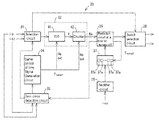
- FIG. 1 illustrates a block diagram for some of a load control device indicating characteristic in accordance with one embodiment of the invention.
- FIG. 2 illustrates a circuit diagram for a load control device in accordance with one embodiment of the invention.
- FIG. 3 illustrates a perspective view indicating a lighting device equipped with load control device in accordance with one embodiment of the invention.
- FIGS. 4 a , 4 b , 4 c , and 4 d illustrate graphs indicating load of above load control device and amount of electricity for each switching element.
- FIGS. 5 a and 5 b illustrate charts for explanation indicating operation of a first conversion method in above load control device.
- FIGS. 6 a , 6 b , and 6 c illustrate charts for explanation indicating detection algorithm for peak value of current in switching element of above load control device and peak value for electricity in load.
- FIG. 7 illustrates a chart for explanation enlarging some of detection algorithm for peak value of current in switching element of above load control device.
- FIG. 1 shows a block diagram of a load control device
- FIG. 2 shows a circuit diagram for a load control device
- FIG. 3 is a perspective diagram appearance of a lighting device equipped with a load control device
- FIGS. 4 a , 4 b , 4 c , and 4 d are graphs indicating load of load control device and amount of electricity in each switching element.
- FIGS. 5 a and 5 b are charts for explanation indicating operation of a first conversion device in a load control device.
- FIGS. 6 a , 6 b , and 6 c are charts for explanation showing detection algorithm for a peak value of a current at switching element/elements of load control device and a peak value of electricity at a load
- FIG. 7 is an enlarged explanation chart showing detection algorithm for peak value of current at switching element of load control device.
- 11 is a lighting device, and this lighting device 11 is equipped with a mechanical body 12 and below the mechanical body 12 is formed a reflection surface 13 .
- a lamp socket 14 is equipped at both longer ends of reflection surface 13 and pipe-shaped fluorescence lamp FL, a discharging lamp as a load, is electrically or mechanically equipped between the lamp sockets 14 .
- a discharge lighting device 16 which turns on discharging lamp as a load control device as shown in FIG. 1 is mounted.
- a power inverter circuit 22 a circuit for turning on discharging lamp, is connected to a DC power part 21 which was rectified and leveled from commercial AC power not shown.
- the power inverter circuit 22 is a half bridge-shaped circuit in which field effect transistor (FET) Q 1 and Q 2 as a switching element is serial connected and inverter current i out0 ( FIG. 4( b )) is passing through.
- FET field effect transistor
- a digital control circuit 23 for a digital controller controlling part as a control circuit is connected to the gate for these field effect transistors Q 1 and Q 2 .
- a serial circuit of a capacitor C 1 for DC cutting and an inductor L 1 is applied to a connection point for field effect transistor (FET) Q 1 and Q 2 and connected to one end of fluorescence lamp FL and one side of the fluorescence lamp FL not shown is connected to a negative pole of the DC power part 21 .
- the fluorescence lamp FL is parallel connected to a starting-up capacitor C 2 .
- the digital control circuit 23 is connected to a gate which is a digital controlling part as a controlling circuit.
- the digital control circuit 23 is connected to a selection circuit 31 selecting electric current i Q1 ,i Q2 ( FIG. 4( c ) and FIG. 4( d )) passing through field effect transistor (FET) Q 1 and Q 2 , and to a first conversion part 32 as the first conversion device and a zero cross detection circuit 33 and a synchronization signal generation circuit 34 .
- a prediction circuit 35 (hereafter called prediction circuit 35 ) is connected to the first conversion part 32 when turning off with prediction device and a correction device, and the prediction circuit 35 is connected to a second conversion part 37 through a rectifying circuit 36 .
- the prediction circuit 35 is connected to the second conversion part 37 by the rectifying circuit 36 .
- electric current values, both of i Q1 ,i Q2 is merely called current value i.
- the selection circuit 31 detects and selects parts through which current is passing among field effect transistors (FET) Q 1 and Q 2 and the selected current is discharged to the first conversion part 32 .
- the selection circuit 31 can be configured in a way that it is forced to select either field effect transistor (FET) Q 1 or Q 2 .
- the first conversion part 32 is connected to a current control oscillator (ICO) 4 (ICO) 41 as an A/D converter and a counter 42 as measuring device one by one.
- ICO current control oscillator
- ICO current control oscillator
- the current control oscillator 41 when current i selected by the selection circuit 31 is input, performs sampling for certain sampling frequency ( FIG. 5( a ) and FIG. 5( b )) which is sampling frequency of the first conversion part 32 , i.e. by 50 MHz frequency and outputs clock signal f corresponding to current value i as a digital amount.
- the current control oscillator 41 outputs high frequency clock signal f when current is high.
- a voltage control oscillator which generates clock signal f by sampling voltage converted by a conversion device from current to voltage on behalf of the current control oscillator 41 by converting current i into its voltage can be used.
- the counter 42 is for counting clock signal f generated by current control oscillator 41 within certain period. Number of counts measured by the counter 42 , for example if switching cycle for field effect transistors Q 1 and Q 2 are 10 ⁇ s (switching frequency 100 kHz) and sampling frequency for current control oscillator 41 is 50 MHz and if time span T sample which is sampling cycle for synchronization signal generation circuit 34 is 0.1 ⁇ s (sampling frequency is 10 MHz), is possible to take about 5, and about 10 if time span T sample , for example is 0.2 ⁇ s (sampling frequency is 5 MHz), and about 50 when time span T sample is 1.0 ⁇ s (sampling frequency is 1 MHz). And counter 42 outputs count number Nn into prediction circuit 35 which is average value for each time span T sample by n intervals.
- the zero cross detection circuit 33 detects zero cross point for current i (point changed correctly at edge) and outputs this detected timing to the signal generating circuit 34 during same period, and this output resets the counter 42 for the current control oscillator 41 and starting timing by same period of signal for each time span T sample generated by the signal generation circuit 34 of same period, and it makes it possible to equalize sampling frequency of the conversion part 32 at cross point of current i.
- sampling frequency of the first conversion part 32 is synchronized in switching frequency of the power inverter circuit 22 ( FIG. 2 ).
- sampling frequency of the first conversion part 32 doesn't necessarily need to be synchronized in switching frequency of the inverter circuit 22 ( FIG. 2 ).
- zero cross detection circuit 33 doesn't necessarily need to be made.
- the rectifying circuit 36 rectifies electricity of fluorescence lamp FL by wave rectification, i.e. AC lamp current i out which is output current and outputs the rectified one into the second conversion part 37 .
- output current or electric power for example, is good as electricity of fluorescence lamp FL.
- the second conversion part 37 equipped with plural number of 2 nd converting method, A/D converter 37 a inside converts fluorescence lamp current i out generated from rectifying circuit 36 into digital amount by A/D converting by controlling A/D converter 37 a. i.e. by slackening each phase to a certain level ( FIG. 6 ( c )). Therefore, the second conversion part 37 carries out sampling by higher sampling frequency than that of A/D converter 37 a. i.e. with lower time span T samp2 than sampling time span of A/D converter 37 a. In addition, second conversion part 37 receives sampling timing from the prediction circuit 35 .
- the second conversion 37 if it is possible to compare with standard analogue amount, and to correct temperature, can substitute each A/D converter 37 a and can be configured in a way that a pair of voltage control oscillator and counter is composed, or only the A/D converter 37 a can be used.
- a switch selection circuit 38 is connected to each gate for field effect transistors Q 1 and Q 2 and controls switching at the time which is predicted by the prediction circuit 35 .
- the switch selection circuit 38 usually controls field effect transistors Q 1 and Q 2 by about 100 kHz of switching frequency (10 ⁇ s of switching cycle)
- Field effect transistors Q 1 and Q 2 is switch controlled by the digital control circuit 23 , and high frequency voltage discharged from the power inverter circuit 22 is converted to resonance voltage of the DC cutting capacitor C 1 , the inductor L and the starting capacitor C 2 and this resonance voltage pre-heats filament of the fluorescence lamp FL and turn on the fluorescence lamp FL.
- the zero cross detection circuit 33 detects the timing current value of i Q1 is actual, and this zero cross detection signal is input to the selection circuit 31 and the selection circuit 31 selects current value, i Q1 , and the selected current value i Q1 is converted to clock signal f corresponding to absolute amount of current by the current control oscillator 41 , and the converted clock signal f is counted by the counter 42 .
- zero cross detection signal from the zero cross detection circuit 33 is input to the synchronization signal generation circuit 34 , and operation timing with the counter 42 is reset to the current control oscillator 41 , and sampling cycle of the current control oscillator 41 (the first conversion part 32 ) is synchronized with switching cycle of the power inverter circuit 22 .
- the prediction circuit 35 calculates differences N D , n based on counting number N n . And it predicts when differences N D, n is less than minimum physical amount N DREF which has generated certain reaction, i.e. when N D,n ⁇ N DREF , predicts ‘turn-off’ timing T to,u for Field effect transistor Q 1 .
- k is usually set to 1 or 2.
- big value is set as k. Lack of this setting resolution is supplemented by doing it this way.
- timing T to,u is predicted within part which is not varied for slope of current passing through field effect transistor Q 1 and if it is impossible to predict timing, T to,u as switching frequency of field effect transistor Q 1 and Q 2 I is varied to a large extent, the prediction circuit 35 , based on absolute amount of pair of counting number N n , predicts the timing when current value i Q1 is peak.
- targeted peak value for current value i is set by difference between lamp current i out and its targeted value.
- this estimator circuit 35 controls the switch selection circuit 38 with slightly small PWM signal of time width T to .
- This switch selection circuit 38 makes the field effect transistor (Q 1 in the present embodiment) that current value i was selected by selection circuit 31 turn off in timing T which it predicted in estimator circuit 35 .
- field effect transistor Q 2 turns on.
- lamp current i out is rectified by the rectifying circuit 36 and each A/converter 37 a of the second conversion part 37 is controlled by multi-rate, and it is converted to digital amount corresponding to certain time span T samp2 after time, ⁇ D1 from timing T to,u .
- the prediction circuit 35 detects peak value for lamp current, i out by converted digital amount, and based on this detection, it suitably corrects minimum reacting physical amount, N DREF .
- digital amount of the second conversion part 37 which is used to correct minimum physical reacting amount, N DREF , for example, it uses average of digital amount converted by each A/D converter, 37 a if time span T samp2 is relatively short, and it uses maximum or minimum value of digital amount converted by each A/D converter, 37 a if time span, T samp2 is relatively long.
- this corrected timing i.e. by the time delayed from detection timing for peak value of lamp current iout to time, ⁇ D2 , the field effect transistor Q 2 is turned off same as ‘turn off control’ of the field effect transistor Q 1 mentioned above, and then the field effect transistor Q 1 is turned ON.
- control for the field effect transistor Q 1 and Q 2 are repeated alternatively by same procedure mentioned above.
- N DREF which generates certain level of reaction
- N D it predicts the timing, T to,u when current values, i Q1 ,i Q2 passing through the field effect transistor Q 1 ,Q 2 reached at peak, and at this predicted ‘turn-off’ timing T to,u , the switch selection circuit 38 turns off the field effect transistor which was ON, i.e. the field effect transistor Q 1 , and at the same time, it turns on the field effect transistor Q 1 which was ON.
- the prediction circuit 35 predicts the timing when current value, i reached at its peak value, and at this predicted timing, switch selection circuit 38 turns off field effect transistor which was “ON state”, here, field effect transistor Q 1 and at the same time, it turns on field effect transistor which was “OFF state”, here, field effect transistor Q 2 .
- switch selection circuit 38 turns off field effect transistor which was “ON state”, here, field effect transistor Q 1 and at the same time, it turns on field effect transistor which was “OFF state”, here, field effect transistor Q 2 .
- N D for counting number N n by corresponding to peak value i of current even based on absolute amount of current i. Therefore it is able to control load more correctly.
- the switch selection circuit 38 turns off field effect transistor Q 1 or Q 2 , therefore it prevents over current due to malfunction of circuits from field effect transistor Q 1 or Q 2
- the first conversion part 32 has same functions as the current control oscillator 41 and the counter 42 .
- the current control oscillator 41 and the counter 42 For example, it's possible to use 8 bit flash-typed A/D converter. In this case, for example, it is possible to use either A/D converter 37 a of the second conversion part 37 , or 37 a of A/D converter of the second conversion part 3 .
- output current or power besides output current such as lamp current i out are possible to be controlled as procedure mentioned above.
- correction device substitute correction of minimum physical amount, N DREF which generates reaction, and it's also possible to control by varying k value of time span, Tsamp 1 , n+k or use both of them simultaneously.
- above the load control device can be used.
Landscapes
- Circuit Arrangements For Discharge Lamps (AREA)
- Inverter Devices (AREA)
Applications Claiming Priority (3)
| Application Number | Priority Date | Filing Date | Title |
|---|---|---|---|
| JP2007275952 | 2007-10-24 | ||
| JP2007-275952 | 2007-10-24 | ||
| PCT/JP2008/068842 WO2009054319A1 (fr) | 2007-10-24 | 2008-10-17 | Dispositif de commande de charge et dispositif d'éclairage |
Publications (2)
| Publication Number | Publication Date |
|---|---|
| US20100264839A1 US20100264839A1 (en) | 2010-10-21 |
| US8415893B2 true US8415893B2 (en) | 2013-04-09 |
Family
ID=40579425
Family Applications (1)
| Application Number | Title | Priority Date | Filing Date |
|---|---|---|---|
| US12/739,716 Expired - Fee Related US8415893B2 (en) | 2007-10-24 | 2008-10-17 | Load control device, and lighting device |
Country Status (6)
| Country | Link |
|---|---|
| US (1) | US8415893B2 (fr) |
| EP (1) | EP2216893A4 (fr) |
| JP (1) | JP5352830B2 (fr) |
| KR (1) | KR101115887B1 (fr) |
| CN (1) | CN101933401A (fr) |
| WO (1) | WO2009054319A1 (fr) |
Families Citing this family (6)
| Publication number | Priority date | Publication date | Assignee | Title |
|---|---|---|---|---|
| US8610369B2 (en) * | 2008-12-30 | 2013-12-17 | Koninklijke Philips N.V. | Electronic circuit for driving a fluorescent lamp and lighting application |
| EP2858222A4 (fr) * | 2012-05-31 | 2017-03-29 | Nagasaki University, National University Corporation | Dispositif de commande pour un circuit de conversion d'énergie |
| DE102012216114A1 (de) * | 2012-09-12 | 2014-03-13 | Bayerische Motoren Werke Aktiengesellschaft | Stromnulldurchgang bei Umrichter |
| KR101723361B1 (ko) * | 2013-08-05 | 2017-04-06 | 주식회사 하이딥 | 조명장치 및 조명장치의 보호방법 |
| DE102015214221A1 (de) * | 2015-07-28 | 2017-02-02 | Robert Bosch Gmbh | Verfahren und Vorrichtung zum Betreiben eines elektrischen Systems, elektrisches System |
| CN111050454B (zh) * | 2019-12-27 | 2023-04-18 | 上海联影医疗科技股份有限公司 | 灯丝电源以及放疗设备 |
Citations (7)
| Publication number | Priority date | Publication date | Assignee | Title |
|---|---|---|---|---|
| JPH06343270A (ja) | 1993-05-31 | 1994-12-13 | Fuji Electric Co Ltd | 予測形瞬時値制御における電流予測方法 |
| JPH09130972A (ja) | 1995-10-26 | 1997-05-16 | Railway Technical Res Inst | 特定周波数成分信号の動作位相算出方法および装置並びにアクティブフィルタのデジタル制御システム |
| JPH1041079A (ja) | 1996-07-25 | 1998-02-13 | Matsushita Electric Works Ltd | 放電灯点灯装置 |
| WO2001078467A1 (fr) | 2000-04-10 | 2001-10-18 | Koninklijke Philips Electronics N.V. | Ballast a detecteur de crete |
| US6963178B1 (en) * | 1998-12-07 | 2005-11-08 | Systel Development And Industries Ltd. | Apparatus for controlling operation of gas discharge devices |
| JP2006049084A (ja) | 2004-08-04 | 2006-02-16 | Toshiba Lighting & Technology Corp | 放電灯点灯装置及び照明装置 |
| US7301376B2 (en) * | 2005-09-29 | 2007-11-27 | Infineon Technologies Ag | Control circuit and method for driving a half-bridge circuit |
Family Cites Families (1)
| Publication number | Priority date | Publication date | Assignee | Title |
|---|---|---|---|---|
| CN1669366B (zh) * | 2002-07-22 | 2010-12-29 | 皇家飞利浦电子股份有限公司 | 气体放电灯驱动器 |
-
2008
- 2008-10-17 WO PCT/JP2008/068842 patent/WO2009054319A1/fr active Application Filing
- 2008-10-17 EP EP08842913.9A patent/EP2216893A4/fr not_active Withdrawn
- 2008-10-17 US US12/739,716 patent/US8415893B2/en not_active Expired - Fee Related
- 2008-10-17 CN CN2008801132068A patent/CN101933401A/zh active Pending
- 2008-10-17 KR KR1020107011281A patent/KR101115887B1/ko not_active IP Right Cessation
- 2008-10-17 JP JP2009538163A patent/JP5352830B2/ja not_active Expired - Fee Related
Patent Citations (7)
| Publication number | Priority date | Publication date | Assignee | Title |
|---|---|---|---|---|
| JPH06343270A (ja) | 1993-05-31 | 1994-12-13 | Fuji Electric Co Ltd | 予測形瞬時値制御における電流予測方法 |
| JPH09130972A (ja) | 1995-10-26 | 1997-05-16 | Railway Technical Res Inst | 特定周波数成分信号の動作位相算出方法および装置並びにアクティブフィルタのデジタル制御システム |
| JPH1041079A (ja) | 1996-07-25 | 1998-02-13 | Matsushita Electric Works Ltd | 放電灯点灯装置 |
| US6963178B1 (en) * | 1998-12-07 | 2005-11-08 | Systel Development And Industries Ltd. | Apparatus for controlling operation of gas discharge devices |
| WO2001078467A1 (fr) | 2000-04-10 | 2001-10-18 | Koninklijke Philips Electronics N.V. | Ballast a detecteur de crete |
| JP2006049084A (ja) | 2004-08-04 | 2006-02-16 | Toshiba Lighting & Technology Corp | 放電灯点灯装置及び照明装置 |
| US7301376B2 (en) * | 2005-09-29 | 2007-11-27 | Infineon Technologies Ag | Control circuit and method for driving a half-bridge circuit |
Also Published As
| Publication number | Publication date |
|---|---|
| JPWO2009054319A1 (ja) | 2011-03-03 |
| US20100264839A1 (en) | 2010-10-21 |
| KR101115887B1 (ko) | 2012-02-17 |
| EP2216893A4 (fr) | 2014-07-09 |
| JP5352830B2 (ja) | 2013-11-27 |
| CN101933401A (zh) | 2010-12-29 |
| EP2216893A1 (fr) | 2010-08-11 |
| WO2009054319A1 (fr) | 2009-04-30 |
| KR20100074299A (ko) | 2010-07-01 |
Similar Documents
| Publication | Publication Date | Title |
|---|---|---|
| US8415893B2 (en) | Load control device, and lighting device | |
| KR101670994B1 (ko) | 역률 보상 회로 및 역률 보상 회로의 구동 방법 | |
| US8754549B2 (en) | Power conversion device | |
| US9167642B2 (en) | LED lighting device and illuminating apparatus using the same | |
| US8791677B2 (en) | Power factor correction circuit for correcting power factor | |
| US10547243B2 (en) | Digital synchronous rectification control for flyback converter | |
| EP2501028B1 (fr) | Alimentation permettant de contrôler le courant | |
| US9287777B2 (en) | Average current controller, average current control method and buck converter using the average current controller | |
| JP2008506347A (ja) | デッドタイムを知的に設定するための方法及び装置 | |
| US10084373B2 (en) | Power conversion device | |
| US10090752B2 (en) | Power conversion device | |
| US10126792B2 (en) | Power converter load current control | |
| US20110007533A1 (en) | Power factor correction circuit | |
| US8686657B2 (en) | Power supply device and light-emitting element drive device | |
| JP5428713B2 (ja) | Dc−dcコンバータ、及びその制御方法 | |
| US6466456B2 (en) | Converter with resonant circuit elements for determing load type | |
| JP4376775B2 (ja) | 共振形コンバータのための回路構成、及び該コンバータを動作させるための方法 | |
| US11968765B2 (en) | Induction cooking system | |
| JP2009303347A (ja) | Dc−dcコンバータの制御回路 | |
| JP2009290812A (ja) | デッドタイム制御回路 | |
| JP4702497B1 (ja) | 多出力スイッチング電源装置 | |
| US20220247325A1 (en) | A resonant inverter and conversion method | |
| JP2009106105A (ja) | スイッチング電源装置 | |
| WO2023209155A1 (fr) | Appareil de commande et procédé de commande de deux commutateurs d'un convertisseur abaisseur de tension synchrone ou d'un convertisseur indirect hybride résonant | |
| JP2021114834A (ja) | 電流検出装置、及び電源装置 |
Legal Events
| Date | Code | Title | Description |
|---|---|---|---|
| AS | Assignment |
Owner name: NAGASAKI UNIVERSITY, JAPAN Free format text: ASSIGNMENT OF ASSIGNORS INTEREST;ASSIGNOR:KUROKAWA, FUJIO;REEL/FRAME:024632/0278 Effective date: 20100510 |
|
| REMI | Maintenance fee reminder mailed | ||
| LAPS | Lapse for failure to pay maintenance fees | ||
| STCH | Information on status: patent discontinuation |
Free format text: PATENT EXPIRED DUE TO NONPAYMENT OF MAINTENANCE FEES UNDER 37 CFR 1.362 |
|
| FP | Lapsed due to failure to pay maintenance fee |
Effective date: 20170409 |